background image

Summary of Contents for SV-3500

Page 1: ...Panasonic e K Audio Division Matsushita Electric Industrial Co Ltd ORDER NO AD8809230T1 D13 ffifcofl Guide L...

Page 2: ...Section 14 4 Signal Processing Circuit 51 5 Audio Section 66 6 Panel Control 77 System Control Circuit 7 101 8 Servo 131 Tape Loading 9 Fewer Supply 136 10 Mechanism 11 141 Troubleshooting Manual 12 1...

Page 3: ...1 General 2 Major Blocks and Operation Function of the SV 3500 1 Major Blocks and Operation 2 h...

Page 4: ...fledged DAT Digital Audio Tape with coaxial and optical digital I O terminals for input output in addition to the analog LINE IN OUT terminals Use of level Furthermore to free level displays SV 3500...

Page 5: ...recording the broadcast satellite modes A and B The SV 3500 is compatible only with mode B at 48 KHz the position of the start ID which is entered at the erases The post recording function for subcode...

Page 6: ...types of data from the panel control circuit signal processing circuit and servo circuit and controls the overall operation of the system This circuit includes the A D and D A converters and mainly h...

Page 7: ...er 11 This DAT OPEN CLOSE RF board chapter 3 Panel control circuit chapter 6 Audio circuit chapter 5 LINE IN OUT DIGITAL IN OUT OPTICAL IN OUT Servo board chapter 8 System control circuit chapter 7 Po...

Page 8: ...3 RF Section 3 1 Block Diagram Description 3 2 Playback Circuit Operation 3 3 Recording Circuit Operation I 5...

Page 9: ...nges the level of the PCM and ATF components of the RF signals for recording pattern of rectangular circuit as signal filter the signal is sent At the waveshaping circuit is waveshaped and then sent t...

Page 10: ...1 and Q352 which are connected to pin 23 of ic on and this grounds the REC side of the heads time Q355 and Q356 on the PB side are off RF signals picked up at the heads are sent to Q353 and Q354 via t...

Page 11: ...pin 3 of connector J27 where used to operate the servo circuit in the servo block RF signals for head A and head B are mixed as shows figure 3 2 2 4 Based on HSW signal control at pin 8 of connector J...

Page 12: ...Z351 SDL4047 5 RPRF I a Operation of control amplifier pin 28 29 and 30 of IC 351 are subjected to equalization by VR354 through VR356 which are connected to the VCA drive circuit as shows in figure...

Page 13: ..._ K25VX ____________Qv ___________03 V 2 5v QV rv ini di j 1C32I AN702IS ENVELOPE the which 27 of IC 351 pin 27 b a c eye is VR354 the IC323 AN8005 REGULATOR IIII 2V 5mi Ji IC 351 pin 30 a ft ____ f__...

Page 14: ...and recording signals 3 At the same time the RF envelope signal which is from pin 14 of IC 321 signal processing circuit to search for the beginning end of tape Its timing chart is shows in figure 3...

Page 15: ...EC GND APB AREC BPB BREC 3 3 4 2 3 4 5 J27 I8IHSW I ll SPRP I7 SRRF I Tree SW Block X R P s w 7X Q353i C351 47 I 7 0354 C352 crT si CO r HL C3 58 crC3S9 fl the signal control the decision to send the...

Page 16: ...s of the PCM signal signal found in the recording signal 3 The recording signals output from pins 18 and 19 of IC 351 sent to pins 3 and 5 of connector J28 through C358 Since the recorder is in the re...

Page 17: ...2 Signal Processing Circuit Operation 4 3 Reference Ciock Generation 1 Playback PH Circuit Operation 2 DF PLL Circuit Operation 3 Master Clock PLL Circuit Operation 4 DIN PLL 4 4 Subcode RAM 4 5 Level...

Page 18: ...he tape is played back the post recording function is used to write the SKIP ID to any part that the user would like to SKIP Once this has been done the tape fast forwards during subsequent playback o...

Page 19: ...ch SIGNAL 1 2 f ch 1 2 f ch ANGLE deg 5 051__ 0 918 3 673 0 459 1 378 2 296 1 378 0 918 58 776 1 378 2 296 1 378 0 918 3 673 0 459 5 051 420 9 76 5 306 1 38 3 114 8 191 3 114 8 76 5 4898 0 114 8 191...

Page 20: ...I Sub Code ID 3 bit Figure 4 1 2 shows the data format of the subcode area which contains the data area 256 bits called the PACK area The subcode data is located in this pack area In one track the dat...

Page 21: ...continuous time code within one recording The table of contents____________________ _______ Year Month Day The day of the week hour Minute Second The catalog number of the cassette_____________ _ The...

Page 22: ...on of the data in the W2 area of figure 4 1 7 the optional code areas Program number Index Start flag Absolute time Program time Catalog number 8 8 8 bit bit bit III Mr 8 8 8 bit bit bit W1 PCM ID ID...

Page 23: ...ure 4 1 9 01 reserved 11 reserved 00 off 01 Pre Emp 10 11 Reserved for orther Pre Emph 00 48 kHz 44 1 kHz 10 32 kHz 11 reserved 00 2 CH 10 11 reserved 00 16bits linear 10 11 reserved 00 13 6pm 10 11 r...

Page 24: ...12 SYNC2 f ch 6 ERASE 130 67KHz 522 67KHz 784 00KHZ 1 568MHz Calculated under the condition that 030 90 warp angle 2000 r p rn cylinder is used EVEN FRAME ADDRESS TRACK 0 5 BLOCK SYNC ODD FRAME ADDRES...

Page 25: ...he following It is necessary for the various circuits in the e g servo circuit system control circuit operate synchronously Various types of clock which become the operating reference for the circuits...

Page 26: ...and IFGA IC s in the signal processing circuit peripheral PLL circuit RAM etc see figure 4 3 The functions of the major IC s are described next There are many types of data recorded onto the tape such...

Page 27: ...4 tn CM e co j z Z Q s CC z ry Q cn Z 8 8 I s cc a Q _ra g 30Hg cm 3MH cm I CD Q I I CDCO I 1 CD CO g CO CM 2 Q Q O i Q 5 CD CD 3 S S i e S O J CD CM a Q D I I i S 8 C CD in CT o5 g o H co E co CO CM...

Page 28: ...Sampling of the SUBID A B track comparison Both tracks are compared if their parity flags are set If they match they are updated If not they are not updated If the parity flags of only one track is s...

Page 29: ...CK parity check Detection of the PLL frequency Correction of the PLL frequency A B tracks Wl and W2 generation in the PCM area Wl and W2 generation in the SUB area Wl and V 2 parity generation PACK pa...

Page 30: ...SIDSH from the SBP For the SUBID s the last correct value in each of the odd even blocks is output Whether the value is correct is determined from the validity flag at the SBP see the SBP function and...

Page 31: ...signal which are used to write the reproduced data to subcode RAM the subcode through signals play rec analog digital II Subcode RAM Control MPX Controls access to the subcode RAM It uses priority cir...

Page 32: ...dulator During DIN demodulated interleave address generation major functions of the DSP are control and conversion of the PCM signal to the during recording I MPX The FS switching signal of the system...

Page 33: ...the data bus SDO SD7 from according to the SUBOE during recording MHz clock and generates i RAM control signal drum synchronization signal TSCK PCM ID Generation Adds the block address frame address a...

Page 34: ...during recording Output the address for syndrome calculation and the address for the RAM read write operation from the ECC to address bus AO A13 based on the control signal from ECC Also output the s...

Page 35: ...codes Duplex error correction for Cl and C2 6 level erasure correction in C2 using the Cl flag Six built in syndrome generators The ECC generates Cl 4 parity bits and C2 6 parity during recording and...

Page 36: ...is at the middle of 1 IC 176 is a buffer amplifier IC 177 is a VCO for the center frequency of 9 408 which is double RSRF 4 704 MHz The playback PLL performs the following functions to The timing char...

Page 37: ...ata Also the operation to write data to the main RAM is performed synchronously with this clock through the DSP However the reading of data from the main RAM and subsequent operations are performed us...

Page 38: ...s n n g O e 5 AX s ss 5 f 2 5 I fiii 125S co 8 o f n 11 s 1 S3 I OT Ou 0 T3 3 5 S a S 0 TJ OT i j Qu t4 CU 3 W O g il u d r i CU 0 e s a 55 Qu Is XZ U I cn o C c tn h aS h s a Qu r Sv 3o 5 r n BHH EO...

Page 39: ...is input from pin 78 of circuit IC 104 the in as r I 13 j_ ri I 2ri Tq i i___ WLprn_ jin_ icio4 63 COSL This circuit playback PLL circuit whenever the contact with the tape e g noise mayby generated P...

Page 40: ...is divided in the DSP to provide various clocks required by the system control circuit and servo circuit 56P R136 C131 470 22P MV If J CTIOI I J60PF Cl30 39P_________ 13k 12 R132 100 Cl 0 1 X 33K AV p...

Page 41: ...10 DIN PLL Circuit 38 and is S Q DFSEL from SBP Digital input DID 9 67 z 63 If To DSP IC101 ToDFPLL IC111 j is applied pulse which VCOA 91 VCOBJ1 92 The DIN Digital Filter PLL operates only when the d...

Page 42: ...n_ O LU CO u CD tn CM i J s g i CM s S X IsS CD x f o I CM CM cd CM p 1 CM in n O i a co CM CO in o g CD x I CM CO iz 5 E CO J t co J CM CD O r T O s Q II CO M CM A T vrco cc X LU o T s S ra F O 82 OT...

Page 43: ...12 Clock Generation II Analog Input Recording 40 1 J E N cc 2 n _ra a 2 g co o 1 5 t o o s X J y LU LU X s 1 n S CD CD CN X CN J Ji o 2 5 8 y g H 3 st I ID r O i i CN Oi co CN p 2 co OJ in 2 tr A i J...

Page 44: ...III Digital Input Recording 41 Q O i s a 5c X g 5 CD in p g I Q g co cn 5 Q Q iz a 5 2 zc 00 CD in CN s g i g g CN s co CN in co g 5 s CN CO CD K CC r lcol p CD CD o c LU CD I I 2 J CN CN CD CN A g i...

Page 45: ...ck o o o o o o 7MCK 7 056MHz o o o 3R5MCK 3 528MHz o o o Table 4 1 42 PLLCP PLL clock pulse PLL 18M PLL 18MHz FCH clock frequency HFCH half FCH DS1FT data shift 48KHz 44 lKHz 32KHz 12 288MHz 11 289MHz...

Page 46: ...ved from heads A and B the data within the RAM is transferred to the system control circuit Data is written to the RAM when RWE is low and read from RAM when ROE is low data received by the DEM IC 102...

Page 47: ...ute time etc and commands sent from the system control circuit After parity codes are added to the data in the subcode area and program addresses are added within the DEM the data is sent to the RF ci...

Page 48: ...d digital music signals are sent to are the the SBP_____ LEVSY C106 LEVDA LEVCK the level Described here are data transfer lines I the panel control H Level meter L Control signal 3R5MCK System clock...

Page 49: ...ignals and level meter signals in the SV 3500 according to its mode Mode data is sent from the system control circuit to the SBP IC 106 and then from the SBP to the IFGA IC 105 Signals are muted at th...

Page 50: ...o co Q O CO I Q co CM CO z o o co I 1 co U U 8 tr g c o co o I ID 5 tr i 1 D O O i i fI I I I I y o 1 3 2 S o n o i LO IR1I 1 ______ L I 5ls e M b E E o o i i i i i i r i i i r i i i i i tr I col I I...

Page 51: ...al Flew During Playback 48 o s ll CD O 0 Q Q O 2 cc cc o o o LU Q _J ro 1 o a S 3 9 o a s 9 c 5 Q I__ J tn o Q g JU f _Q Q Q O UJ I Q I I 8 CN CN O S og t 3 8 1 I I I I f Q __S Q S LU Q co co S tn co...

Page 52: ...o cn 2 cc i i i i i i I i i i 2 cr I I i 3 o 5 C 5 a s o 8 9 8 9 Is 8 y Q Q Q CO CN O cz ra ra O o co o LU Q Q I fs Lt CC CD ft g Q m a 5 o V I Ilf I l Lt in i a a s S I L X Th i i i j 03 E a S Q QJ r...

Page 53: ...ording 50 I Q r i i i i L o Q 5 cc 2 O Q cc 5 in i Q Q 3 o S s y 55 Q CC cc co II o co o CD r J O 8 y 5 y I t I OJ O O o ro ro TJ _o O n o LU I s Q Q i T 1 co i Q Q co OJ CD x Tn i i i ____ i TTW A m...

Page 54: ...5 Audio Section 5 1 Recording Circuitry Block Description 5 2 Recording Circuitry Operation 5 3 Level Switching Circuit 5 4 Playback Circuitry Block Description 5 5 Playback Circuitry Operation 51...

Page 55: ...level lifier filter DifferentialRecording OdB amplifier balance A I Sampling A D Amplifier hold converter r I I J Jo AW The level switching circuit inputs the preamplifier s output and detects if the...

Page 56: ...B transformed passes 2 and amplification is performed sent to pin 1 of low pass filter of IC 403 unwanted components above the frequency range KHz and higher are removed to prevent loopback The charac...

Page 57: ...vel of the signa switch is input by LINE IN The timing chart for the sampling operation is shows in figure 5 2 4 The sampling frequency is 96 KHz or double the standard 48 KHz This is used to smooth t...

Page 58: ...6 IC419 C 5 J7 12 256FS IC419 A IC419 B 2 J6 j4 ADD J7 bl lr Input signal at pin 7 of IC 407 1 The analog signal from the sampling hold circuit passes R439 and is input by pin 1 of A D converter IC 41...

Page 59: ...IC 419 A If it is lower than 12 dB it is sent to pin 4 of IC 426 through IC 421 and IC 419 B and C 3 At digital filter IC 426 the left channel data input by pin 5 are rearranged into a serial signal S...

Page 60: ...converter since its linearity deteriorates The level switching circuit is designed to improve these two characteristics 3 However if the signal is lower than 12 dB switches A and B are both set to po...

Page 61: ...ms when the recording level drops to below 12 dB 1 00 s h R486 777 4 When the recording level is higher than 12 dB pin 13 of IC 422 is low and pin 12 is high Thus pin 11 is low Conversely when the re...

Page 62: ...nal when recording level is lower than 12dB Figure 5 3 4 59 IC426 Pin 16 SH Circuit level switching point delayed by the one shot multivibrator IC401 3 I I I__ R417 2 7K R419 3 3K IC419 Pin 3 IC403 2...

Page 63: ...is output as a low signal from pin 9 of IC 417 B This output causes pin 4 of IC 419 C to go low The digital data signal from pin 3 of IC 419 B passes from pin 5 to pin 6 of IC 419 C Figure 5 3 5 shows...

Page 64: ...e two extra bits truncated by the gate ON signal when the recording level is below 12dB within IC 421 LSB circuit in IC 419 B IC426 Pin 41 DINL IC423 fl gain is 4 times the original when the recording...

Page 65: ...e of data signal 3 At the D A converters the PAM signa which was D A converted by D A 1 and D A 2 is generated The PAM signals are combined amplified by differential amplifier Muting LINE Class AA Lo...

Page 66: ...t is a playback data signal than 12 dB with respect to the 2 The playback data signal from pin 9 of IC 501 is input by pin 12 of 4DAC processor IC 502 At IC 502 the operation changes according to the...

Page 67: ...the 4DAC processor is activated by an input signal which is lower than 12 dB with respect to the full scale level pin 9 of IC 507 goes high and the gain of amplifier IC 511 B becomes 12 dB Further whe...

Page 68: ...ts above 22 KHz removed is output from pin 2 of IC 513 and sent to amplifier IC 703 The output from IC 703 pin 7 is separated and applied pin 3 of IC 705 A and pin 6 of IC 705 B The IC 705 A and IC 70...

Page 69: ...cuit 3 Key Scan and Remote Control Input Circuit 4 FL Displays and LED Indicators 6 3 Test Program Function 1 Procedure 2 Operation 66 1 Display 2 All Display Mode 1 FL Display 2 LED Indicator 3 Level...

Page 70: ...lh control unit I v1601 36 45 47 62 11 12 J3_ 14 22 Numeric keypad S601 S620 The front panel keys configured as key matrix are scanned and signals from the wired remote control are received The panel...

Page 71: ...nal level data 4 LEVSEL is the read enable signal for the level signal 5 15 msec 5 msec LEVSEL 7 16 LEVCK LEVDA R14 Rl 0 denotes invalid data Figure 6 2 2 Input Data Timing Chart 68 LEVDA is the 15 bi...

Page 72: ...13 C602 47p R602 1K I i I 150m i h 1 il__ i 2 C602 and R602 comprise a differentiator A spike is generated at point a C610 changes and approximately 1 ms later a high level signal generated at point...

Page 73: ...r Play S639 Music x S628 K ___ S629 x End Search S630 Erase Re start num ID S623 Write start ID S624 J Write start ID S625 x __ edit S626 Etose skip ID S622 Analog S604 x _ _ S610 X nltotj S607 Coun _...

Page 74: ...s The display refersh timing is performed as follows meter data refreshes the level meter display FL during the next display period after both left and right are sampled every 15 ms LED refreshed each...

Page 75: ...al auto d d d d ana log Pins 36 through 62 of IC 603 are output as segment data The grids and segments are shows below mem ory 48kHz 44 1kHz 32kHz skip 1D digi tai start 1D time g I 1 i 8 8 next o o I...

Page 76: ...proximately 2 s This level is memorized by panel control IC 603 c The input signal also varies during the peak I display Level display is performed according the real time signal level However if a la...

Page 77: ...off 4G is completely lit 0 2 s and turned off 5G is completely lit 0 2 s and turned off 2G right channel level meter is completely lit for 0 2 s 3G is completely lit 0 2 s and turned off See Table 6 2...

Page 78: ...in Fig 6 3 1 Analog LED D630 lights 1 2 3 4 5 6 See Fig 6 3 1 playing I fl k fl program number When an operating key is pressed while figure 6 3 1 is displayed its key code is displayed in the sec num...

Page 79: ...switch Key code Operating key Operating switch Timer 1 S603 memory S616 counter reset S614 erase start ID S623 digital S605 analog S604 auto P No S620 recall S619 counter mode S615 end search S630 mu...

Page 80: ...3 4 Power off Unload Circuit 5 7 3 1 Signal Processing Circuit 2 Servo Circuit 3 Panel Control Circuit Analog Circuit RF section audio section 4 Other Circuits 7 4 1 Dew Sensor and Heater 2 Reset Sig...

Page 81: ...t and mechanism control circuit are both located on the digital board As shows in figure circuits are connected to the peripheral circuits This chapter deals mainly with the system control mechanism c...

Page 82: ...TE power mute Clocks 7 MCK 7 056 MHz TSCK 33 3 Hz SEGCP 66 6 Hz NBLK BLKSEL SRRF rec signal SRPR rec play switch NSPRDY ready signal for data transfer RSRF play signal ATT attenuator signal NEMP empha...

Page 83: ...VR202 the photocouplers i at the passes on 5V 1C118 B 2 The transparent phototransistor time the tape where 1 ight phototransistor is off and VR203 are used to adjust the sensitivity of since there ar...

Page 84: ...hickness detection Figure 7 2 2 Hole Positions on Cassette 82 TH2 TH3 THl TH2 TH3 TH4 TH5 For ordinary tape and music tape detection For erasure prevention tab detection THl r i TH5 th4 757g The casse...

Page 85: ...The detected information is input by pins 10 through 17 of IC 107 51 TH1 52 TH2 Hole present Switch off 53 o TH3 54 o TH4 Hole absent 55 TH5 S6 S2 J___ I ____ I I I 1 O I S6 _____________ _______ 1 F...

Page 86: ...tape 17 TH4 Tape type Record inhibited 16 TH5 Cassette absent 15JTH6 3 Mechanism Mode Detection Circuit 12V IC117 4 MMODO PC4 41 MM0D1 PC5 46 MMOD2 l_ Figure 7 2 5 Mechanism Mode Detection Circuit 84...

Page 87: ...te is loaded in the mechanism Stop 3 Light emitter board Light emitter board LED 42JMODO I 41 MODI j 40 MOD2 Light detect I board I_______ 2 The state combination detection Mechanism Mode of the mecha...

Page 88: ...sette loading motor is 119 3 The supplies from pins 7 the motor power supply 23 MFWD MMOD 1 The Off 2 The on or off state of Q105 connects voltage dividing R116 which is connected to R115 used to swit...

Page 89: ...or stop H II H L L L 87 Mode Motor Drive Cassette Loading Motor Drive Drive System 23 MMOD 24 MFWD Unde fined Unde fined During Cassette Loading Motor Drive Unde fined Unde fined 10 JUT1 During Mode M...

Page 90: ...ntermediate position 37 OPEN IC107 Pin 37 GND IC107 Pin 38 38 CLOSE 0PEN Cam gear as viewed from above After the cassette loading motor has been activated the detection switches leaf switches linked t...

Page 91: ...pstan up the This circuit unconditionally unloads the cassette to protect the tape and cylinder when the power is turned off with the cassette loaded When the power is turned off NRST1 and NPMUTE of p...

Page 92: ...are transferred through the data bus SPDTO through SPDT7 IC106 SBP IC105 IFGA i such number track IC107 System control b NSPSTB NSPCS 7MCK TSCK NSPRDY 42 12 20 21 22 120 81 This section describes the...

Page 93: ...ontrol s operating mode c End code system control to SBP One byte is sent as a code which informs the that transfer has completed or 26 system _TL ZX LF jn_ I I 1 1 I Time code out Start p I during en...

Page 94: ...the Servo Section 92 IC107 System control IC104 Digital servo J13 fl 9 51 52 Tzi CAPER RLFGTU RLFGSU 3 4 39 mode switching signal for the analog circuit High PLAY Low REC BLKSEL Command which determin...

Page 95: ...rs long periods such as still unload subcodes ID frame control etc 6 SRVDTO through SRVDT5 are data lines which determine the rotation speed of the capstan and cylinder An example for atandard speed o...

Page 96: ...ching command It is low when synchronized with ATF during PLAY and high when not synchronized with ATF REC FF etc Capstan rotation command High forward Low reverse 8 NCAPSL and NRELSL are latch comman...

Page 97: ...switching signal for the reel High Standard Low down x 1 2 Approach mode is a signal which makes SPE in order to quicken the drop of the ATF The output conditions are a Activation of the PLAY mode b...

Page 98: ...NPRDY 96 a Operating key input signal b Remote control information NTRCLK is a serial transfer clock 110 25 KHz is a ready signal for data transfers from panel control to system control circuit lines...

Page 99: ...of IC321 in the R F section i vthJ 12 IC110 1 RFENV detects the envelope of the RF output signal High Envelope present Low Envelope absent 3 NEMP is a signal used to apply deemphasis during PLAY depen...

Page 100: ...current to the heater to evaporate any dew when it forms This is done to prevent the possibility of the tape sticking to the head when there is dew on the cylinder issues a command to the mechanism co...

Page 101: ...V 5V 5V Figure 7 4 3 Timing Chart for Reset Signal 99 System control IC107 76 RSTOUT J4 1 NRST1 IC104 62 J9 9 NRST2 1 The signals at various points are as shows in figure 7 4 3 NRST2 To panel control...

Page 102: ...he subcode area may be affected when the 130KMAD signal goes high during post recording 130KMAD which is sent from the signal processing section enters pins 8 and 9 of IC 123 and becomes an inverted s...

Page 103: ...ntegrating Circuit 2 Low Frequency Compensation Circuit ATF Servo Operation Circuit Description Based on Block Diagram Sampling Pulse Timing Pilot Signal Peak and Di fferential Pi 1ot Voltage Detector...

Page 104: ...C for supply reel and controls the reel speeds so that A B C To ensure the deck reads subcode information of the tape at high tape speeds the reel servo circuit controls capstan motor rotation so tha...

Page 105: ...in 9 IcypgI in IC211 capstan FG CPFGlI waveform shaper I I _ I I I To servo IC s pin 8 cp FQl To servo IC s pin 2 CYFG To servo IC s pin 3 IrlfgtI TO servo IC s pin 4 rlfgs t40mv Capstan FG magnetic r...

Page 106: ...utilizing the phase difference between FG1 and FG2 processed within the servo circuit IC 104 The cylinder FG signal is generated by an FG provided on the cylinder motor 1 Reel FG signals are generated...

Page 107: ...ocity phase L PLAY mode CAPED __ Forward reverse conrrand w pwmcapA 5 sy I TorqueY ccarmandl Fi 777 SRVDL ATF on off ccmrand o IC 204 Capstan PWM output EC A TorqueHO command J 25 In REC mode the caps...

Page 108: ...upled to 104 s internal speed control logic 49 SRVDT 3 48 SRVDT 2 46 SRVDT 0 a In REC mode pin 85 of the system controller IC 107 and pin 60 SRVMD of the servo controller are both set to high which pl...

Page 109: ...C 208 via IC 203 Capstan control J Velocity ri control Yj Phase i control i Capstan PWM output IC208 Capstan motor driver Armature coil 2 Capstan Servo in PLAY Mode In PLAY mode the capstan servo cont...

Page 110: ...command signal from main servo controller IC 104 o o IC205 1 1 I 1 AAAr 1 It J8 IC205 1 11 IF S 11 1 __ I C240_ IC206 4 IC 203 pin To capstan driver IC 208 via IC 203 pin l fl Z 1 u JI r Rv i i A B 1...

Page 111: ...s differentiating capacitor When IC 205 s pin 10 is high it yields a high pulse which shorts pin 8 of IC 205 to pin 9 This discharges C240 and prevents adverse affects from torque caimand switching me...

Page 112: ...always tracks the center of the current track track 1 is being played in this sequence If the level of fl on track 4 is indentical to that on track 2 the play head is tracking the center of the main...

Page 113: ...F signal Envelope signal on Block Diagram 784kHz I T r CN O_ Q_ GO ATF control signal The signal recording on tape is picked up by the rotary heads and applied to high pass filter HPF Z322 via an RF c...

Page 114: ...rence in the peak levels is nullified velocity and ATF control signals for this purpose supplied from IC 201 to capstan motor driver IC 208 In the mean time the playback signal takes another part to b...

Page 115: ...either of the tracks SP1 samples the pilot read untraced track from the two adjacent tracks SP2 samples that read off the already track SP1 is used sampling the peak levels of the pilot signal pickud...

Page 116: ...fset caused by mechanical loads the ATF system etc b Purpose SPE is used for controlling capstan motor speed so that the play head always tracks the center of the track even if the recorded tracks on...

Page 117: ...tracted by BPF Z323 and applied to pin 8 of IC 201 I I I I I I I I I I Peak Det Differential pilot voltage detector ATF TER envelope signal IC 201 ATF block diagram SP1 JULIU O SP2 JUUL b The pilot si...

Page 118: ...head is tracking a non recorded blank sampling clocks SP1 and SP2 are not applied to Vspe signal created from the SPE It is used to slightly increase such non recorded blanks so that ATF as the head s...

Page 119: ...rotation command ttt SRVDL ATF on off command A PG ly PG Forward Reverse ccnrnand The cylinder rotation speed command is applied to pins 46 through 51 of the servo controller IC 104 as with the case o...

Page 120: ...Cylinder rotation speed command is applied to pin 46 through 49 of the servo controller IC 104 The following shows the command bit status i H i H The cylinder FG and PG signals are applied to pins 2...

Page 121: ...OFF if low ON if high 13 IC205 2 When IC 205 is off R256 and R259 are not included in the feedback loop letting the amplifiers provide the normal servo gain When IC 205 is on R256 and R259 are insert...

Page 122: ...x200 x 150 t CYLGAIN 5V 0 Figure 8 7 3 124 100 ms in FF 50 ms in REW Tape Speed command from system controller x wo x 150 T Multiplication I of speed X50 X25 x 25 X75 x50 x 100 X75...

Page 123: ...ecified for a specific search speed SRVDL AFT OiX OFF command IC208 capsta motor driver f r FG signa pulses are counted within IC 104 and the of the supply and takeup FG pu3 se counts is Pins 46 throu...

Page 124: ...controller issues the next velocity command for x50 to the mechanism controller which then transfers the corresponding velocity conmand to the servo controller IC 104 s pin 46 High 47 High Condition f...

Page 125: ...37 This circuit forcibly unloads the tape if Turned off in any mode FF than the STOP mode IC 208 capstan motor driver o Torque command forward reverse 0 1 ED S the deck is REC PAUSE other Reference vo...

Page 126: ...s si ack on the 1 The torque limiter TL command servo controller s pin 79 is normally high It is set to low only for tape unload 2 The RL TLK reel torque command system controller s pin 21 is normally...

Page 127: ...12 of J5 2LRT v To switching regulator Triangular wave Pcwer block 1 1 The 2LR signal 96 KHz twice the L R switching signal frequency is applied from the signal processor to 202 This circuit supplies...

Page 128: ...ure 8 11 1 130 Signal processing block System controller block HSW head switching TSCK 1 2 rotation NCYK1 cylinder lock 1 NCYKO cylinder lock 2 SPEMSK sampling clock mask RLFGTU takeup reel FG RLFGSLI...

Page 129: ...e Loading 1 Top View of Loading Mechanism 2 Bottom View of Loading Mechanism 9 2 Loading Operations and Functions 1 Tray Close Sequence 2 Tray Open Sequence 1 131 9 1 Loading Mechanism Layout and Func...

Page 130: ...oading Mechanism 132 Half arm prevents reverse insertion of tape Dew sensor senses dew condensation on the mechanism Cassette receiver cassette tape is loaded here Joo o 15 Holder arm drives the holde...

Page 131: ...OPEN CLOSE switch is pressed when the tray is in the open position the system processor IC 107 is informed The processor then applies command voltages to pin 3 and 10 of the tray motor drivers IC 115...

Page 132: ...the gear engages slot of Figure 9 2 7 At the End of Tray Close Operation the control plate pin ribes on the tapered cam on the bottom side of the cam gear the cassette holder is onto loading mechanis...

Page 133: ...provided for the tray close sequence to pin 3 and 10 of the tray motor drivers IC 115 and IC 119 which then drive the tray motor The tray motor drives the pulley gear via a belt If the OPEN CLOSE swit...

Page 134: ...10 Power Supply 10 1 Block Diagram 10 2 Motor Drive Power Supply 10 3 Muting Circuit 136...

Page 135: ...5V 1 D12 D15 5 D62 J3 GND 6 AC 5 3V 5 4 27V D16 3 5 0V 2 F5 5V IC14 1 H2V Q11 J4 5V 5 GND 4 IC15 7 6V 3 2 NPMUTE Q12 NRST1 1 J5 12 D19 Q13 IC51 11 Q51 10 Q52 9 T T 8 1 2 3 6 7 4 5 137 z 3 Muting circu...

Page 136: ...matic of Switching Regulator 138 R53 820 C54 16V47 C86 50V 3 3p L C55 50V3 3 the the IC51 1 2 aw R57 L51 H C51 16V100 L51 D52 To J5 f csujz R55 390 1 C52 16V 100p IC51 1 2 AN6919 I 6 The cylinder and...

Page 137: ...respectively where they are compared with each other appearing at IC 51 s varies its pulse width depending on tape speed The square wave signal appearing at Q51 s collector is then smoothed by L51 an...

Page 138: ...oint B i i Power ON Power OFF I 10K At power on off the muting circuit puts the system CPU into a muting state to suppress pop noise output to the LINE OUT jacks LEVEL METERS or PHONES jack Also at po...

Page 139: ...act Layout 2 Mechanism Compact Operation 11 3 Mechanism Mode Transition Timing 141 11 4 Mechanism Operation and States in Different Modes 11 5 Upper Cylinder Head and Cyliner Block Replacement 11 2 Me...

Page 140: ...apstan o o Cassette sensing switch L 3 bit switch used to detect the material and thickness of the cassette tape Supply reel base L supplies tape in PLAY mode rewinds tape at high speed in REW mode FG...

Page 141: ...assembly submechanism 143 1 2 3 Remove the capstan belt 1 Take off the two PB angle screws 2 Remove the four screws retaining the assembly 2 Bottom Side of View l The fol lowing figure shows a bottom...

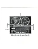
Page 142: ...3 Submechanisin Assembly reel base side Figure 11 4 Submechanism Assembly reel base side 144...

Page 143: ...4 Bottom Side of Main Chassis 2 I Figure 11 5 Bottom Side of Main Chassis 2 145...

Page 144: ...e loading into the deck To take up tape slack during tape unloading this mode is used only in transitions from STOP 1 mode In this mode the deck is ready tepe loading or is in STOP mode after tape unl...

Page 145: ...R in the direction of the arrow 147 The actuator plate slides sidewise as the cam gear rotates The components linked to the actuator plate are driven by the sliding actuator movement The mechanism co...

Page 146: ...ntact the pinch arm is swing by the actuator and of the of the post roller is brought into with point b of the pinch roller arm and pushes up the pinch roller in the direction of arrow v b After this...

Page 147: ...es the reel lock in the direction of arrow 4 to 1ock up the supply reel and REW modes is accomplished when as the driving gear rotates in the CW 5 FF Idler Operations The figure below shows a step in...

Page 148: ...The following figure shows the play arm actuator shaft actuator plate positions for the mechanism modes which reel arm take up The cam gear slot drives the brake arm A in the vertical direction This e...

Page 149: ...gear s cam the pin on the brake arm C pushes up the trigger arm As a result the trigger arm claw is engaged with the intermediate pulley rack causing only the brake arm C to trip in the direction of a...

Page 150: ...stable tape transport the soft brake is mechanically controlled to regulate the back tension to the supply reel base by detecting the tape roll diameter on the supply reel roll diamenter on the supply...

Page 151: ...lock off Capstan off STOP3 STOP2 STOP1 A Take up tape slack STOP3 Cassette is ejected the 29 0 Mode motor Soft brake off PAUSE STOP1 STOP2 Unloading A Reel brake off ___________________ Figure 11 17...

Page 152: ...ion is detected STOP1 mode i Mode motor rotates in unloading direction Reel brake released i FF idler engaged i Mode switch in STOP2 position is detected Mode motor stops Take up reel base starts rota...

Page 153: ...round the cylinder by means of post rollers In the STOP 1 mode the reel and soft brakes are applied to the reel bases STOP1 mode Mode motor starts in loading direction Reel lock turned on FF idler eng...

Page 154: ...xl speed reel lock idler released Pinch roller is pressed capstan runs at speed In PLAY mode capstan control is switched into AFT The soft brake PLAY idler and FF are aid in position to the tape a co...

Page 155: ...0 Reel is detected FG control Capstan motor rotates x200 i Capstan motor rotates Mode motor rotates in loading direction Trigger brake applied FF idler released Mode switch in PAUSE position detected...

Page 156: ...00 rpm To relieve v tape running load 2 REW into PAUSE Mode For transition from mechanism first goes Capstan motor rotates x 200 4 Capstan motor rotates x 200 Mode motor rotates in loading direction T...

Page 157: ...Mode motor stops STOP1 mode Cylinder rotates 2000 rpm Open command During unloading the supply reel is locked up by the reel lock Reel brake released FF idler engaged t Mode switch in STOP2 position i...

Page 158: ...Removing the Cylinder Block Remove the grounding lead screw 1 Remove the three screws 2 3 and 4 retaining the cylinder These screws should be retightened in the order of 2 3 and 4 Figure 11 27 Cylinde...

Page 159: ...n the figure above by alternately putting the deck in the PLAY and STOP modes and verify that the top and bottom edges of the tape are free from creases Adjust Pl P2 P5 and P7 with the HV 30 fixture b...

Page 160: ...ders nave rounding adjust post roller P2 kk kk Envelope shoulders dotted circles should have no rounding If these shoulders have rounding adjust post roller P5 TP804 20 mV Div 5 ms Div Normal CH 2 AC...

Page 161: ...1 PC Board Layout Signal Flow 2 Block Diagram 3 General Power On Flow 4 Detailed Power On Flow 5 Troubleshooting Manual 1 Capstan 2 Cylinder 3 Reel 4 ATF 5 Mode Motor 163 6 Cassette Loading 7 Defecti...

Page 162: ...shaping FWU ED Mechanism Lower PCB Digital PCB 164 Servo analog Vs 2LRT switching reference Jll J12 J13 J14 Mechanism controller VM motor voltage Mechanism mode DOT EOT PWM output from FG and PG perio...

Page 163: ...rfaced and sent to the motor driver DFG DPG o I integration and J low frequency compensation DFG and DPG control circuit With respect to V the counter emf which is generated in proportion to the speed...

Page 164: ...rformed when key is pressed Is mechanism gear sound heard Does mechanism gear sound repeat Tape defective Cassette defective Cassette switch defective Mode motor system Capstan system Cylinder system...

Page 165: ...u E 0 X s J y e a M U E Hi X o n U o o n Q U u U D a in D tn D w w o o Cu v U o in o s H KJ E d o CM O W in c 0 1 o u 1J E 0 X o E a a ex fl u 21 I a s a c H g H u g fl 81 a J E u X 21 a s u I v X5 2...

Page 166: ...Capstan FG Capstan rotation command Capstan PWM output Are CADFG1 and CADFG2 output when the cassette is removed and rotated by hand repeated or full Is PWM deceleration deceleration 1 No Rotation if...

Page 167: ...d CYDPG output the driver Is VM within 3 to 6 V Is VS within 1 5 to 3 5 V Is 2LRT output properly 169 Is CYDPG output properly 30Hz 1 2 3 4 5 Is PVJM output abnormal e g repeated deceleration and acce...

Page 168: ...F REW time code can t be read Is the reel FG output 1 Reel FG RLDFGT RLDFGS 2 Unloading torque command RLTLK TL Trouble during loading e g etc Is the reel FG output Is TL low Does RCTLK change Except...

Page 169: ...T F P C M A T F S U B 0 SNYC SPf SP2 generation The ATF is the control signal used to keep the head on track during playback The pilot signal from the RF circuit is sliced with the SYNC signal and the...

Page 170: ...ack 1 sama Check for scratches 2 stuck the to 3 flow The value changes p p 4 Is ATFOFS output Is the SYNC signal output 5 6 Are SP1 and SP2 output with correct timing 7 Is SRVDL low during playback 17...

Page 171: ...motor output Types of Trouble 1 No mode transition direction of 2 Mode motor does not stop due to overrun 173 Trouble relating discribed Is the mode motor power supply 7 6 V Is the BA6238A output vol...

Page 172: ...Closes immediately even if opened 174 Is the power supply 7 6 V Command CLDNTR CLDN4MTR OK does immediately 1 Cassette loading motor power supply 7 6V BA6238A digital PCB Are command output from the c...

Page 173: ...transport due to damaged tape 5 Abnormal operation due to improper tape transparency BOT and 5 The also be at fault for Check the Are the LEDs for EOT and BOT on Turns on off when the light path is b...

Page 174: ...ent 3 ATF Gain Adjusment 4 RF Recording Level Adjustment 5 Playback PLL Adjustment 176 7 Recording Adjustment 1 ADC Offset Adjustment 2 ADC MSB Adjustment 6 Playback Adjustment 1 DAC Output Balance 2...

Page 175: ...ears The delayed sweep is 50 jasec 177 2 channel 30 MHz oscilloscope with external trigger and delay sweep and with a 10 1 probe Blank tape for recording and playback conmercially available blank tape...

Page 176: ...ope waveform r ff ATF 522kHz bsbmhhhhhbbi jL Jlj r I i 7 I Enlargement of CH 2 to the leading edge of the 0 04 msec of the label on the standard tape 5 Rotate VR201 located on the mechanism board and...

Page 177: ...pr aaa The adjustment is correct if the error rate value is 100 or lower If this value continues to be above 100 proceed to step 3 Display range is from 0000 to 9999 shows above when of CH 2 OROT2 en...

Page 178: ...1 J12I10 p p or higher J102 9 ATFOFS 50 mV 5 0 5 V _ msec 50 jusec CH 1_____ DC VR321 Volts Div Time Div Delay____ Trigger AC GND DC Ajustment Point 7 Adjust VR355 so that the amplitude of the output...

Page 179: ...ps 1 7 CH 1 CH 2 VR351 CH1 VR352 CH2 65mVp p Note Steps 1 4 are temporary adjustments AC__ VR351 AC__ VR352 Volts Div Time Div Delay____ Trigger AC GND DC Adjustment Point TP351 J28 2 5 mV 2 TP352 J28...

Page 180: ...2 Head B JL IL I 11 7 I 1 1V 1 If not VR351 and adjustment portion 7 The adjustment is correct if the amplitude of the waveform at J12 10 is within 0 8 to 1 1 V head current back the 20 mV 0 5V 2 msec...

Page 181: ...hich the music can be played back by turning CT170 in the clockwise and counterclockwise directions set CT170 to the center of the range 2 Adjust CT170 on the signal processing board to the point wher...

Page 182: ...e level meter moves to 20 dB O o o Digital voltmeter 1 DAC Output Balance Load a blank tape for recording check that the playback output is 20 dB 0 2 dB with respect to 0 dB at 1 KHz Adjust VR503 for...

Page 183: ...the left channel TP502 for the right channel 1 Set the recorder to ANALOG IN in the stop mode signal input 7dBV 20dBI o o o 1 Use a signal generator to feed a signal to ANALOG IN 4 Adjust VR401 for th...

Page 184: ...t into the RD SE01 transparency tape a 2 Connect 3 Connect 186 EOT pin 6 of J14 to the oscilloscope and adjust VR202 so that the output is 3 5 V BOT pin 6 of J13 to the oscilloscope and adjust VR203 s...

Page 185: ...e GLU 37 RRQT Inputs the read request signal from the GLU 38 GND For ground connection 39 TEST This is the terminal for IC test Normally this is for ground connection 40 NEXT For syndrome calculation...

Page 186: ...ls for memory addresses O 67 A13 VCOPL Not used open 68 O Not used open 69 PLL4 0 70 PLL3 Not used open PLL2 0 71 Not used open 72 PLL1 O Not used open PLLD 0 73 Not used open PLLC 74 I Outputs the PL...

Page 187: ...his terminal inputs the digital signal DIG I 1 SIDSH I This terminal inputs the shift clock signal for the sub code ID 2 3 SIDDA This terminal inputs and outputs the serial data for the sub code ID I...

Page 188: ...190 Pin No Outputs the data of the digital IN during recording Outputs the shift clock signal of ID code during playback Outputs the shift clock signal of the main ID during recording Outputs the shif...

Page 189: ...terminal 12 288 MHz I O 87 CXAO 88 CXBI I O Crystal terminal 11 2896MHz 89 CXBO 90 VCOIN Inputs the PLL clock signal for digital input 91 VCOA 0 Outputs the PLL phase comparison signal for digital in...

Page 190: ...for syndrome calculation of the sub code S SCLK 17 Input the sub code data LSB MSB For output of the ST 1 signal of the sub code not used open 26 SST1 0 0 For output test not used open 0 For output t...

Page 191: ...t the ECG program counter RST 61 Inputs the termination signal of the syndrome calculation 62 DF 1 Inputs the C1 and 02 switching signals 63 DF 2 This is the output terminal to start the syndrome calc...

Page 192: ...signal of the capstan FG 250 pulses rev 9 CYPG 1 Inputs the signal of the cylinder PG 1 pulse rev 10 VOD To be connected to 5V NC 11 Not used open 12 Vss For ground connection 13 TC Not used open 14...

Page 193: ...s the SRVD latch command of the capstan NCPSL 45 Input the summed data of the reel FG speed 52 Vss For ground connection 53 NLNROK Not used open 54 Vod To be connected to 5V NCPK O 55 Outputs the data...

Page 194: ...Outputs the 73 5kHz PWM of the capstan motor Outputs the command for the rotation direction of the cylinder 82 CYLED 0 PWMCYL 83 O Outputs the 73 5kHz PWM of the cylinder motor 84 Vdd I To be connecte...

Page 195: ...31 GND For ground connection 32 TP1 For input test not used open 33 VDD2 To be connected to 5V 34 TP2 For input test not used open 35 TP3 36 PLL VAR O 37 PLL18M 38 ADD I Inputs the A D data 39 DFD O O...

Page 196: ...s the PLL clock signal for the digital input VCDIV 63 64 DIGO Inputs the digital signal Inputs the synchronous detection signal of the playback signal MSYNC 65 Inputs a signal for the parity check of...

Page 197: ...s For ground connection 1 I O These are addresses and data buses NSPSTB 10 Inputs the strobe signal for signal processing OFSCP 11 12 NSPRDY O This is the output terminal for the data transfer 13 SBPT...

Page 198: ...tputs the control data enable signal LEVSY 0 45 LEVSF Outputs the control data shift clock signal 46 0 Inputs the serial control data and outputs the serial level meter data LEVDA 47 I O DFSSEL O 48 T...

Page 199: ...rvo 19 NRELSL O Outputs the gain down control signal of the cylinder servo 20 CY GAIN O This is the output terminal to control the speed and phase of the capstan servo 21 RLTLK O 22 NC Not used open 2...

Page 200: ...supply reel 52 RLFGSU I O These terminals are addresses and data buses NC Not used 66 SPDTO I O Address and data bus NC Not used open TRCLK 71 I O For input and output of the serial data RXD 72 Input...

Page 201: ...used Outputs the attenuator signal ATT O 97 0 98 BLKSEL 99 NC Not used 0 100 NEMP Outputs the emphasis signal 101 NC Not used 102 O Output the summed data of the reel FG speed 109 Vdo To be connected...

Page 202: ...ntrol signal This is the input terminal to connect with the condenser of the NF loop 18 NFC VCC 1 To be connected to 5V 19 This is the input terminal to connect with the ATF circuit 20 SRVDL NC Not us...

Page 203: ...es rev RLDFGS 37 Outputs the supply reel FG signal 40 pulses rev O RLFGS 38 Inputs the supply reel FG signal 40 pulses rev RLFGS 39 To be connected to 5V 40 Vcc 2 Outputs the capstan FG signal 250 pul...

Page 204: ...This is the input terminal of the signal for the rate of the frequency division At a High level or when this terminal is open f CKIN 256fs At a Low level f CKIN 192fs The ADC control signal is out pu...

Page 205: ...rd At a High level or when this terminal is open LR serialA At a Low level LR parallel Outputs the data of the right channel OPARA L The deglitch signal of DAC OPARA H This is the input terminal of th...

Page 206: ...ds the serial data 14 TXD I Receives the serial data O 19 INT 1 Inputs the remote control signal INT2 LEVSY 20 Inputs the control data enable signal 21 CNVss For ground connection 22 RESET Input the r...

Page 207: ...C Not used open 0 Output the signal for the display tube 0 Output the signal for the display tube 63 Vcc I To be connected to 5V 64 65 Vss For ground connection 0 Output the signal for the key scan an...

Page 208: ...Printed in Japan K880900600MIZUTA...

Reviews: