background image

ORDER No.AD0201005C3

Portable MD Player

SJ-MJ50GH

MD unit: RAE1619Z-M Mechanism Series

Colour

(S)...................Silver Type

SPECIFICATIONS

Specifications

1

Summary of Contents for SJ-MJ50GH

Page 1: ...ORDER No AD0201005C3 Portable MD Player SJ MJ50GH MD unit RAE1619Z M Mechanism Series Colour S Silver Type SPECIFICATIONS Specifications 1 ...

Page 2: ...aker output level 55 mW 55 mW 16 Speakers 3 6 cm 16 x2 Power supply Rechargeable battery DC 1 2V included rechargeable battery Battery DC 1 5V One LR6 AA UM 3 battery Dimensions WxHxD Cabinet dimensions 79 9x72 7x13 7 mm incl projecting parts 81 1x74 6x14 9 mm Weights 97 g with battery 70 g without battery Play time Approximate operating time in hours in hold mode at 25 C on a flat stable surface ...

Page 3: ... the rechargeable battery included is fully recharged AC adaptor and charger AC adaptor input AC220 V 50 60 Hz 5W AC adaptor output and Charger input DC 3 5 V 0 5A Charger output DC 2V 0 5 A Recharging time About 3 5 hours Notes The play time may be less depending on the operating conditions Specifications are subject to charge without notice Weight and dimensions are approximate 1 1 Accessories S...

Page 4: ...BD000020 External battery case 1 pc K3ZZ00200041 Nickel metal hydride rechargeable battery 1 pc RFKFHFAZ01EM Soft case 1 pc RFC0069 H Speaker battery carger 1 pc L0EAAB000002 AC adaptor 1 pc N0JCBD000001 2 Precaution of Laser Diode 4 ...

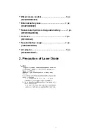
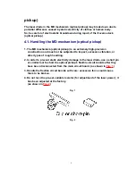
Page 5: ...3 Operating Instructions 4 Handling Precautions for MD Mechanism Optical 5 ...

Page 6: ...tion and must not be subjected to impact excessive vibration or other types of rough handling 2 In order to prevent static electricity damage to the laser diode use a short pin or similar tool to short the optical pickup s flexible circuit boards after they have been disconnected from the main circuit board as shown in Fig 1 3 Handle the flexible circuit boards with care excessive force could caus...

Page 7: ...s shown in Fig 3 2 Work table grounding Put a conductive material sheet or steel sheet on the area where the traverse deck optical pickup is placed and ground the sheet as shown in Fig 4 Caution The static electricity of your clothes will not be grounded through the wrist strap So take care not to let your clothes touch the traverse deck optical pickup Fig 3 7 ...

Page 8: ...section describes procedures for checking the operation of the major printed circuit boards and replacing the main components For reassembly after operation checks or replacement reverse the respective procedures Special reassembly procedures are described only when 8 ...

Page 9: ...fter replacing the main components optical pickup or traverse motor etc of mechanism unit block change to the adjust mode and then perform the adjustments Laser power off set ROM RAM 5 1 Checking for the P C B 9 ...

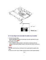
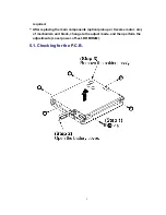
Page 10: ... Check the P C B as shown below 10 ...

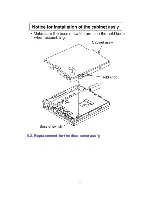
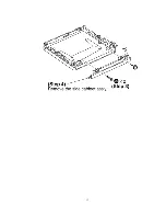
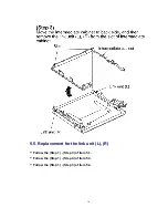
Page 11: ...5 2 Replacement for the disc cover ass y 11 ...

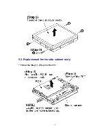
Page 12: ...5 3 Replacement for the side cabinet ass y Follow the Step 1 Step 3 of item 5 1 12 ...

Page 13: ...13 ...

Page 14: ...5 4 Replacement for the intermediate cabinet Follow the Step 1 Step 3 of item 5 1 Follow the Step 1 Step 4 of item 5 3 14 ...

Page 15: ...15 ...

Page 16: ...5 5 Replacement for the link unit L R Follow the Step 1 Step 3 of item 5 1 Follow the Step 1 Step 4 of item 5 3 Follow the Step 1 Step 3 of item 5 4 16 ...

Page 17: ...17 ...

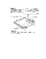
Page 18: ...5 6 Replacement for the traverse motor Follow the Step 1 Step 3 of item 5 1 18 ...

Page 19: ...19 ...

Page 20: ...20 ...

Page 21: ...5 7 Replacement for the optical pickup Follow the Step 1 Step 3 of item 5 1 Follow the Step 1 Step 4 of item 5 6 21 ...

Page 22: ...22 ...

Page 23: ...23 ...

Page 24: ...24 ...

Page 25: ...25 ...

Page 26: ... block change to the adjust mode and then perform the Laser power adjustment Off set automatic adjustment and Playback onlydisc magneto optical disc automatic adjustment 6 1 Instruments to prepare 1 Playback only disc Test disc RFKV0006 2 Commercially available recordable disc fully recorded with music magneto optical disc 26 ...

Page 27: ...in part replacement procedure 5 2 Replacement for the intermediate cabinet 2 Move the optical pickup to the innermost side and attach the disc cover 3 Set the battery and connect the remote controller 4 Turn off the power and switch main unit s HOLD switch off 5 Press the VOL VOL and keys on the remote controller within two seconds asshown in Fig 5 Fig 5 6 When the adjustment mode is activated T0J...

Page 28: ...nd T3J You must perform the adjustment by observing the order T0J T1J T2J T3J 6 2 2 Laser Power Adjustment Adjust each laser power read power for reading play 6 2 2 1 Set the Unit to the Adjustment Mode Cautions About handling the optical pickup and the magnetic head The optical pickup is structured precisely therefore it is very fragile Be careful not to touch it with the edge of the laser power ...

Page 29: ...areful with the static electricity 6 2 2 2 Adjustment Procedure 1 Uncover the laser power meter as shown in Fig 6 Fig 6 2 Make T0J display on the LCD of remote controller and locate the sensor of the laser power meter at a position above the optical pickup horizontally at a level of the disc position as shown in Fig 7 Fig 7 29 ...

Page 30: ... adjustment procedure with the read power exceeding over 660 W will result in damage to the optical pickup 6 Set the laser power with the key of the remote controller LP changes to LDOK in the LCD 7 Press the key of the remote controller LDOK changes to T0J on the LDC 8 Remove the laser power meter Laser power adjustment is finished REFERENCE For use of MD cartridge type laser power meter We recom...

Page 31: ...printed circuit board are exposed as shown in Fig 8 2 Set the laser power meter cartridge as shown in Fig 8 3 Set the battery and attach and secure the battery cover with a rubber band as shown in Fig 9 4 Follow the steps for 6 2 1 Enter the adjustment mode Subsequent procedures are the same as those for the sensor type Fig 8 Fig 9 31 ...

Page 32: ...r If there is no abnormality FOK will be displayed 5 Pressing the key while FOK is displayed will return to the T1J display mode 6 2 4 Magneto optical disc automatically adjustment 1 Have T2J indicated on display and set the full recorded magneto optical disc Check to make sure the disc is properly seated 2 Press key of the remote controller The adjustment is started 3 During adjustment AADJ is di...

Page 33: ...ide in the order 4 Press key OOK or ONG changes to T3J 5 After the adjustment is finished remove the disc 6 2 6 How to get out the adjustment mode Remove the battery when you finish the adjustment 6 3 Checking the main unit s keys 1 Set the battery and connect the remote controller 2 Turn off the power and switch main unit s HOLD switch OFF 3 Press the VOL VOL and keys on the remote controller wit...

Page 34: ... to O 5 After all keys have been pressed and there is no abnormality T OOO will be displayed 6 Perform below voltage check about the keys come under if it is not displayed T OOO Main unit s keys Check points ON OFF HOLD TP428 0V 2 2V IC201 48pin 0V 2 2V TP421 1 13V 2 2V TP421 1 69V 2 2V VOL TP421 0V 2 2V VOL TP421 0 58V 2 2V Note Refer to 10 Printed Circuit Board Diagram for the test points 7 Remo...

Page 35: ...35 ...

Page 36: ...36 ...

Page 37: ...37 ...

Page 38: ...38 ...

Page 39: ...39 ...

Page 40: ...40 ...

Page 41: ...41 ...

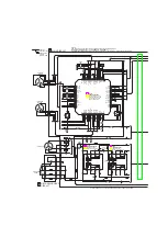
Page 42: ...8 Schematic Diagram Notes 8 1 Type Illustration of IC s Transistors and Diodes 42 ...

Page 43: ...ending on theinternal impedance of the DC circuit tester No mark MD STOP MD play 1kHz L R 0dB Important safety notice Components identified by mark have special characteristics important for safety Furthermore special parts which have purpose of fire retardant resistors high quality sound capacitors low noise resistors etc are used When replacing any of components be sure to use only manufacture s...

Page 44: ...Voltage and signal line Positive voltage line Playback signal line 9 Schematic Diagram 10 Printed Circuit Board Diagram 11 Block Diagram 12 Terminal Function of IC s 12 1 IC1 C1BB00000640 RF AMP 44 ...

Page 45: ...l band pass filter switcing input terminal 14 SETR I Band pass filter control input terminal 15 GND GND terminal 16 LDD O APC output terminal 17 LDS I I V converted laser quantity of light input terminal 18 LDREF I Laser control signal input terminal 19 VC O 1 2VCC reference voltage output terminal 20 VR I 1 2VCC reference voltage input terminal connected to GND through capacitor 21 WOO O Wobble s...

Page 46: ...erminal 35 EQI I RF equalizer input terminal 36 RFO O RF signal output terminal 12 2 IC101 C1BB00000639 ATRAC ENCORDER DECORDER SERVO SIGNAL PROCESSOR Pin No Mark I O Division Function 1 VDD I Power supply terminal 2 SLCO O HF signal slicing level output terminal 3 SLCISET I Slicing level adjustment bias resistor terminal 4 EFMIN I HF signal input terminal 5 TEST1 I Test terminal 6 RESET B I Syste...

Page 47: ...l 20 DD I Tracking error signal input terminal 21 AVDD1 I Power supply terminal 22 AVSS1 GND terminal 23 ADIPWO I Wobble signal input terminal 24 NC Not used open 25 NC Not used open 26 NC Not used open 27 SIN I Connected to GND through reistor 28 SOUT Not used open 29 SCLK Not used open 30 VSS Connected to GND 31 VDD I Power supply terminal 32 NC Not used open 33 LDREF Laser power control signal ...

Page 48: ...t used open 49 NC Not used open 50 MD2 DRAM data in output trminal Not used open 51 NC Not used open 52 VSS GND terminal 53 MCASB DRAM data in output terminal Not used open 54 MOEB DRAM data in output terminal Not used open 55 NC Not used open 56 NC Not used open 57 TEST3 I Test terminal 58 SPPWMF O Spindle PMW output terminal 59 SPPWMR O Spindle PMW output terminal 60 VSS GND terminal 61 VCC2 I P...

Page 49: ...utput terminal Not used open 74 FOK O Focus OK signal output terminal 75 FAST FAST signal output terminal Not used open 76 VDD I Power supply terminal 77 CL I CPU I F data transfer clock input terminal 78 CE I CPU I F chip enable signal input terminal 79 DI I CPU I F data input terminal 80 DO O CPU I F data output terminal 81 WRQB O CPU interrupt signal output terminal 82 INTB O CPU I F interrupt ...

Page 50: ...ction output terminal 95 LRCO O Lch Rch clock output terminal 96 DDATA O Voice extend data output terminal 97 BCO O Bit clock output terminal 98 MAD9 DRAM CAS signal output terminal Not used open 99 NC Not used open 100 MAD8 DRAM address output terminal Not used open 101 MAD7 DRAM address output terminal Not used open 102 MAD6 DRAM address output terminal Not used open 103 NC DRAM address output t...

Page 51: ...ress output terminal Not used open 112 MAD10 DRAM RAS signal output terminal Not used open 113 NC Not used open 114 SMON3 I Monitor signal output terminal Not used open 115 SMON2 O Monitor signal output terminal 116 SMON1 O Monitor signal output terminal 117 SMON0 Monitor signal output terminal Not used open 118 TEST2 I Test terminal 119 SHOCK O CHOCK RFNG output terminal 120 VSS Connected to GND ...

Page 52: ...input terminal F 6MHz 14 VSS Connected to GND 15 XI Sub clock input terminal Not used connected to GND 16 XO Sub clock output terminal Not used open 17 MMOD Memory mode switching input terminal Not used connected to GND 18 REM_DATA O LCD driver data output terminal 19 LINK_IN I LINK serial data input terminal 20 Not used open 21 Not used open 22 Not used open 23 Not used open 24 BUZZER O Beep sign...

Page 53: ...29 CHARGE O Recharge control output terminal 53 ...

Page 54: ... F read data input terminal 38 SSCLK O IC101 I F clock output terminal 39 SELAD O IC101 I F address select output terminal 40 RESET B O IC101 I F reset output terminal 41 ZDTCL I IC101 I F monitor signal input terminal 42 ZDTCR I IC101 I F monitor signal input terminal 43 Not used open 44 BATT_SW O Battery control signal output terminal 45 Not used open 46 Not used open 47 Not used open 48 PLAY_KE...

Page 55: ...sed open 62 GHSW O ROM RAM gain switching signal output terminal 63 LDON Laser ON OFF switching signal output terminal H ON L OFF Not used open 64 RFCONT O RF AMP power supply control output terminal 65 P CONT O Power supply control output terminal H Power OFF L Power ON 66 MOD_CNT O Power supply switching IC control output terminal 67 MODEL 1 I Model switching input terminal 1 68 MODEL 2 I Model ...

Page 56: ...ED control output terminal 12 4 IC301 C0GBZ000009 FOCUS TRACKING COIL TRAVERSE MOTOR DRIVE ROTALY DETECTOR Pin No Mark I O Division Function 1 IN1R I H bridge 1 logic reverse output terminal 2 CP1 O Charge pump gain puls output terminal 3 CPC1 I Charge pump gain input terminal 4 CP2 O Charge pump gain puls output terminal 5 CPC2 I Charge pump gain input terminal 6 VG O Charge pump gain output trmi...

Page 57: ...omparator output terminal 18 SWO O 3 phase sled W output terminal 19 SCOM I Sled driver block position detection comparator output terminal 20 WOUT O 3 phase spindle W output terminal 21 VOUT O 3 phase spindle V output terminal 22 COM I Spindle motor COM point connect input terminal 23 UOUT O 3 phase spindle U output terminal 24 FG O FG pulse output terminal 25 RF Output current detection input te...

Page 58: ...X VCO highest frequency setting input terminal Connected to GND through resistor 37 IN2R I H bridge 2 logic reverse input terminal 38 IN2F I H bridge 2 logic forward input terminal 39 MUTE I H bridge 1 2 and 3 phase sled mute input terminal 40 VS2 I H bridge 2 motor power supply input terminal 41 OUT2F O H bridge 2 forward output terminal 42 OUT2R O H bridge 2 reverse output terminal 43 PGND1 GND ...

Page 59: ... Ass y as Replacement Parts Please take note of the following points relating to Battery Carrying Case to be used for protection of Rechargeable Battery Ass y from shorting Replacement Parts Rechargeable Battery Ass y RFKFHFAZ01EM supplied will be provided with Battery Carrying Case RFA0475 Q No replacement parts will be supplied for Rechargeable Battery Ass y without Battery Carrying Case Replace...

Page 60: ... Fig 11 15 Replacement Parts List Notes Important safety notice Components identified by mark have special characteristics important for safety Furthermore special parts which have purposes of fire retardant resistors high quality sound capacitors low noise resistors etc are used When replacing any of components be sure to use only manufacture s 60 ...

Page 61: ...5 1 BRL1A1CWB TRAVERSE MOTOR 1 5 2 RHD14074 SCREW 1 5 3 RJC99038 RECHARGE BATT TERMINAL 1 5 4 RMX0156 1 STOPPER RUBBER 1 5 5 XQN14 B2FC SCREW 1 6 RAF2000A 4M OPTICAL PICKUP 1 7 RXJ0025 DRIVE SHAFT 1 8 RHD14067 SCREW 5 9 RJC99039 1 RECHARGE BATT TERMINAL 1 10 RJR0195 2 BATTERY SHAFT 1 11 RGK1448 K INTERMEDIATE CABINET 1 12 RHQ0083 S SCREW 6 13 RXQ0829 LINK UNIT R 1 14 RXQ0830 LINK UNIT L 1 14 1 RGU...

Page 62: ...104K 10V 0 1U 1 C106 ECJ0EB1A104K 10V 0 1U 1 C107 ECJ0EB1A104K 10V 0 1U 1 C108 ECJ0EB1H102K 50V 1000P 1 C113 ECJ0EB1A104K 10V 0 1U 1 C115 ECJ0EB1A104K 10V 0 1U 1 C116 ECUE1C822KBQ 16V 8200P 1 ECJ0EB1C822K C117 ECJ0EB1H102K 50V 1000P 1 C130 F1H0J1050013 6 3V 1U 1 C201 ECUE1C103KBQ 16V 0 01U 1 F1G1C103A044 C202 ECUE1H101KBQ 50V 100P 1 C203 F1J0J4750005 6 3V 4 7U 1 C204 ECJ0EB1A104K 10V 0 1U 1 C206 E...

Page 63: ...1A224KBV 10V 0 22U 1 F1H1A224A001 C516 ECUV1A224KBV 10V 0 22U 1 F1H1A224A001 C517 F1J0J4750010 6 3V 4 7U 1 C523 F5A421040001 4V 0 1U 1 C601 F1G1H221A416 50V 220P 1 C602 F1G1H221A416 50V 220P 1 C603 ECUE1H101KBQ 50V 100P 1 C604 ECUE1H101KBQ 50V 100P 1 C605 ECUE1H101KBQ 50V 100P 1 C606 ECUE1H101KBQ 50V 100P 1 C607 F3E0G106A001 4V 10U 1 C608 ECJ0EB1A104K 10V 0 1U 1 C609 F3E0G106A001 4V 10U 1 CP1 RJS2...

Page 64: ...NSISTOR 1 2SD1819ASL Q202 B1ADNB000003 TRANSISTOR 1 Q203 DTC114YETL TRANSISTOR 1 B1GBCFJN0001 Q401 B1CFNC000001 TRANSISTOR 1 Q402 XP152A12C0MR TRANSISTOR 1 B1DHAC000002 Q403 XP152A12C0MR TRANSISTOR 1 B1DHAC000002 Q404 B1CFNC000001 TRANSISTOR 1 Q405 XP151A13A0MR TRANSISTOR 1 B1DFBC000003 Q406 2SB1218ASTX TRANSISTOR 1 2SB1218ASL Q407 2SB1218ASTX TRANSISTOR 1 2SB1218ASL Q408 XP4601TX TRANSISTOR 1 XP0...

Page 65: ...J103 1 4W 10K 1 ERJ2RMJ103X R302 ERJ2GEJ1R0X 1 4W 1 1 ERJ2RMJ1R0X R303 ERJ2GEJ682X 1 4W 6 8K 1 ERJ2RMJ682X R305 ERJ2GEJ393X 1 4W 39K 1 ERJ2RMJ393X R401 ERJ2GEJ225X 1 4W 2 2M 1 ERJ2RMJ225X R402 D1H447420001 470K 1 R403 D1H447420001 470K 1 R404 ERJ2GEJ274X 1 4W 270K 1 D0GA274JA001 R405 ERJ2GEJ105 1 4W 1M 1 D0GA105JA001 R406 D1H84744A024 470K 1 R407 ERJ2GEJ103 1 4W 10K 1 ERJ2RMJ103X R408 ERJ3GEYJ101V...

Page 66: ... HOLD 1 K0D112B00071 SX201 EVQPUL02K SW VOLUME 1 SX203 04 RSG0051 P SW SKIP SEARCH 2 SX206 RSG0051 P SW PLAY STOP 1 X101 H2D169500019 OSCILLATOR 1 X201 H2D400400010 OSCILLATOR 1 Z401 RJH9212 1 CONNECTOR TERMINAL 1 K4BC02E00007 Z402 K4ZZ01000154 CONNECTOR 1 16 Cabinet Parts Location 17 Packaging 18 Schematic Diagram for Printing with A4 size 66 ...

Page 67: ...H020200000 KA AM 1 2002 Matsushita Electric Industrial Co Ltd All rights reserved Unauthorized copying and distribution is a violation of law 67 ...

Reviews: