
Summary of Contents for SJ-MD150
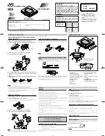
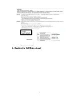
Page 5: ...4 Caution for AC Mains Lead 5 ...
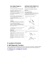
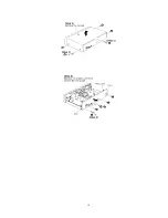
Page 10: ...10 ...
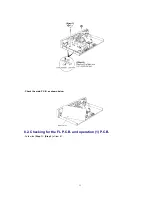
Page 15: ...15 ...
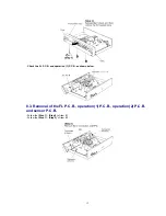
Page 16: ...16 ...
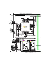
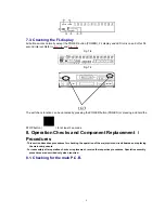
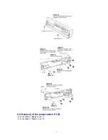
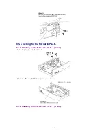
Page 17: ... Check the MD servo P C B B side as shown below 17 ...
Page 19: ...19 ...
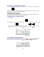
Page 20: ...20 ...
Page 21: ...21 ...
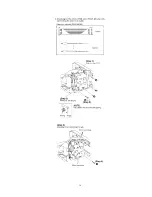
Page 22: ...8 7 Replacement for the belt and loading motor Follow the Step 1 Step 3 of item 8 1 22 ...
Page 23: ...23 ...
Page 25: ...25 ...
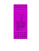
Page 36: ...30 TEST02 Test terminal Not used open 36 ...
Page 48: ...48 ...
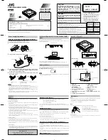
Page 57: ...20 MD Mechanism Unit Parts Location 57 ...
Page 58: ...21 Packaging 58 ...
Page 59: ...F000300000YM KH 59 ...