Summary of Contents for SJ-HD515
Page 8: ...8 ...
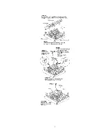
Page 9: ...9 ...
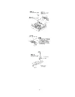
Page 10: ...10 ...
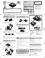
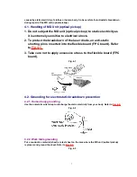
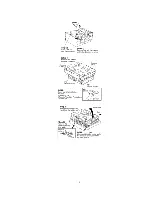
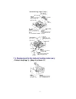
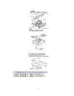
Page 11: ...7 4 Replacement for the belt and loading motor ass y Follow the Step 1 Step 3 of item 7 1 11 ...
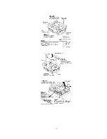
Page 12: ...12 ...
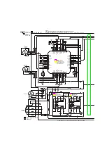
Page 14: ...14 ...
Page 46: ...F000306000YM KH 46 ...