© Panasonic Corporation 2010. All rights reserved.
Unauthorized copying and distribution is a violation of
law.
PSG1010008CE
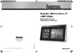
Digital Photo Frame
Model No.
MW-20EB
MW-20EG
Product Color: (K)...Black Type
TABLE OF CONTENTS
PAGE
PAGE
1 Safety Precautions
-----------------------------------------------
3
1.1. General Guidelines---------------------------------------- 3
1.2. Before Repair and Adjustment ------------------------- 4
1.3. Protection Circuitry ---------------------------------------- 4
1.4. Safety Part Information----------------------------------- 4
2 Warning
--------------------------------------------------------------
5
2.1. Prevention of Electro Static Discharge (ESD)
to Electrostatically Sensitive (ES) Devices---------- 5
2.2. Service caution based on Legal restrictions -------- 6
2.3. Caution for use of Battery ------------------------------- 6
3 Service Navigation
-----------------------------------------------
7
3.1. Service Information --------------------------------------- 7
3.2. Troubleshooting Guide ----------------------------------- 8
4 Specifications
----------------------------------------------------
12
5 Location of Controls and Components
------------------
13
5.1. Main Unit Key Button Operations---------------------13
5.2. Remote Control Key Button Operations ------------14
6 Operating Instructions
-----------------------------------------
15
6.1. Media Information ----------------------------------------15
6.2. About the internal memory, CDs and SDs --------- 16
6.3. Preparation for power source ------------------------- 17
6.4. Connecting/Recharging an iPod/iPhone ----------- 18
6.5. Connection to PC ---------------------------------------- 19
7 Self Diagnostic and Doctor Mode Setting
--------------
20
7.1. Service mode --------------------------------------------- 20
7.2. Doctor mode----------------------------------------------- 24
8 Disassembly and Assembly Instructions
---------------
29
8.1. Disassembly flow chart --------------------------------- 30
8.2. Types of Screws------------------------------------------ 31
8.3. Main Parts Location Diagram ------------------------- 31
8.4. Disassembly of Bottom Case Unit ------------------- 32
8.5. Replacement of Speaker (1) -------------------------- 33
8.6. Replacement of Speaker (2) -------------------------- 35
8.7. Disassembly of Main P.C.B. --------------------------- 37
8.8. Replacement of Top Case Unit ----------------------- 40
8.9. Replacement of Rear Panel Unit--------------------- 43
8.10. Disassembly of IR P.C.B. ------------------------------ 45
8.11. Disassembly of Panel P.C.B.-------------------------- 46
Summary of Contents for MW-20EB
Page 13: ...13 5 Location of Controls and Components 5 1 Main Unit Key Button Operations ...
Page 14: ...14 5 2 Remote Control Key Button Operations ...
Page 16: ...16 6 2 About the internal memory CDs and SDs ...
Page 17: ...17 6 3 Preparation for power source ...
Page 18: ...18 6 4 Connecting Recharging an iPod iPhone ...
Page 19: ...19 6 5 Connection to PC ...
Page 31: ...31 8 2 Types of Screws 8 3 Main Parts Location Diagram ...
Page 62: ...62 ...
Page 82: ...82 ...