


© Panasonic System Networks Co., Ltd. 2012
Unauthorized copying and distribution is a violation
of law.
ORDER NO. KM41201532CE
F13
Telephone Equipment
Model No.
KX-TG7731S
KX-TG7732S
KX-TG7733S
KX-TGA470S
Link-to-Cell Cellular Convergence
Solution
S: Sliver Version
(for U.S.A.)
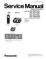
(Handset)
KX-TGA470S
KX-TG7731S
(Base Unit)
(Charger Unit)
Model No
Base Unit
Handset Charger Unit Expandable
KX-TG7731 1 (TG7731) 1 (TGA470)
Up to 6
KX-TG7732 1 (TG7731) 2 (TGA470)
1
Up to 6
KX-TG7733 1 (TG7731) 3 (TGA470)
2
Up to 6
KX-TGA470*
1 (TGA470)
1
Configuration for each model
*KX-TGA470 is also an optional accessory, which contains a
handset and a charger.


