background image

ORDER NO.ISD0110009S0

G20

Service Manual

Front Counter Register

JS-170FR-**

© 2001 Matsusita Communication Industrial Co., Ltd.
All right reserved. Unauthorized copying and
distribution is a violation of law.

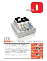
Summary of Contents for JS-170FR Series

Page 1: ...ORDER NO ISD0110009S0 G20 Service Manual Front Counter Register JS 170FR 2001 Matsusita Communication Industrial Co Ltd All right reserved Unauthorized copying and distribution is a violation of law ...

Page 2: ......

Page 3: ...h Design and specifications are subject to change without notice Caution 1 High voltage is applied to inverter transformer cable and capacitor on the backlight PCB and backlight connector shown in Fig 1 below Do not touch those parts without switching off JS 170FR expect for probes of oscilloscope or tester for testing or repairing purpose only Fig 1 Do not touch the parts within this spot without...

Page 4: ... begin Yellow 64 N A Fujitsu 1 2 266MHz Not Standard JS 170FR U23 June 2001 Gray 64 N A Fujitsu 1 2 266MHz Not Standard 120V JS 170FR U25 September 2001 USA Gray 64 N A Fujitsu 1 2 333MHz Not Standard JS 170FR G20 From begin Yellow 16 DOS 6 22 Gen 2 266MHz Not Standard AC Cable Straight JS 170FR G22 July 2001 Friendly Gray 64 DOS 6 22 Gen 2 266MHz Standard AC Cable L type JS 170FR G24 September 20...

Page 5: ...n Gray 64 N A Fujitsu 1 2 333MHz Standard AC Cable L type JS 170FR A20 From begin Yellow 16 DOS 6 22 Gen 2 266MHz Not Standard JS 170FR A22 June 2001 Gray 64 N A Fujitsu 1 2 266MHz Not Standard JS 170FR A24 September 2001 Australia Gray 64 N A Fujitsu 1 2 333MHz Standard JS 170FR A23 June 2001 Gray 64 N A Fujitsu 1 2 266MHz Not Standard JS 170FR A25 September 2001 Australia Gray 64 N A Fujitsu 1 2...

Page 6: ...play enhanced From 2400 bps to 9600 bps except G version 01B 01B 01B 01B 6 Operating System Not pre installed except G version 01B 01B 01B 01B 7 Power supply modified Manufacturer changed 01D 01D 01D 01D 8 Power supply modified Diffuser panel added 02A 02A 02A 9 CN1 Not implemented 01D 01D 01D 01D 10 IDE interface buffer IC18 23 not implemented 01D 01D 01D 01D 11 LAN LSI driver software version up...

Page 7: ...om 3 25 GB to 5 GB 01F 01F 01F 13 LAN driver software Software modified 01J 01J 01J 14 Lower case modified 1 Battery replacement simplified 00F 00A 15 Lower case modified 2 Rubber foot frame reinforced 02B 02B 02B 02B Modifica tion No Reason for modification 1 R430 jumper wire imbedded 2 Measures against locking up during LAN communication 3 Brightened CRT connected to VGA output 4 User demand 5 U...

Page 8: ...ck circuit 2 9 2 1 2 3 IDE interface 2 10 2 1 2 4 USB interface 2 12 2 1 3 Main RAM circuit 2 13 2 1 4 BIOS ROM 2 14 2 1 5 IT8673F circuit 2 15 2 1 5 1 IT8673F Pin Assignment 2 16 2 1 5 2 Serial port COM1 2 2 18 2 1 5 3 Parallel port interface circuit 2 20 2 1 5 4 FDD interface circuit 2 21 2 1 5 5 Keyboard controller circuit 2 23 2 1 5 6 PS 2 mouse controller circuit 2 25 2 1 6 Serial port COM3 4...

Page 9: ...2 GATEARRAY Pin Assignment 2 51 2 1 19 Optional interface Refer to the page 4 5 CN7 2 54 3 Test Program and Power Supply Check 3 1 3 1 Voltage checks on the MAIN PWB 3 1 3 2 Oscillation frequency check 3 2 3 3 POWER switch FRONT switch check 3 2 3 4 Backup function check 3 3 3 5 Current consumption check 3 4 3 6 BIOS setup 3 4 3 7 Method of diagnostic program starting 3 9 3 8 Execution of diagnost...

Page 10: ......

Page 11: ...0 SVGA specifications standard using a color LCD It is provided with a 20 digit x 1 line or 2 line fluorescent display tube for customer display In addition it has an interface of up to 2 channels for a Cash Drawer System Configurations Example J B J B HUB J B VGA Monitor Card Reader 170FR 150MS Printer TM 88 CCU 150DC 170CD ISP ISP 170MG 160RD CCU Communication Control Unit ISP In Store Processor...

Page 12: ...512KB Type Flash memory Fujitsu MBM29F040 or compatible Drives Floppy disk drive Option external One 3 5 type drive unit 1 44MB 720KB Standard internal One 2 5 type EIDE drive unit 4 0GB or more Hard disk drive Option internal One 2 5 type EIDE drive unit Clock Tolerance Monthly 3 minutes Temperature 25 C Back up Method Real Time Clock RTC Battery Lithium battery 560mAh Battery life 8 years need t...

Page 13: ...dness 60 Load 200g Frequency 5 Hz Interface Serial interface using internal COM4 TTL level Size 12 1 type Local Area Network Interface Ethernet 10BASE T 100BASE TX Speed 10M 100Mbps Connector 8 pin Modular Jack RJ 45 Wake on LAN Supported Magnetic Card Reader Option U24 U25 type Track ISO1 ISO2 Swipe speed 10 120 maximum cm s Maximum swipe speed will be reduced when dual track reader is used Inter...

Page 14: ...uency 50 60 Hz Connectors No Interface Number Connector type 1 Serial 3 COM1 2 9pin D sub connector male COM3 8pin modular connector NOTE COM3 is shared with Customer Display interface It is possible to switch between Customer Display and External COM3 port by software 2 Cash Drawer 1 6pin DIN connector female 3 Parallel 1 25pin D SUB connector female 4 Video 1 15pin D SUB connector female VGA 5 L...

Page 15: ...2mm Depth 320 mm 12 6 inches Height 365 mm 14 4 inches with rubber foot Weight Approx 10 kg Tilt angle 15 35 Material Case body Stainless steel sheet Top cover ABS Supported OS Microsoft MS DOS Windows 95 Windows NT Workstation 4 0 Accessory AC cable 1pc 2 5m Safety Standard Safety Standard TÜV UL EMI FCC Part15 Class A CISPR Class B CE C tick ...

Page 16: ...RAM 640K FFFFFFFF FFFE0000 10000000 01000000 00100000 000E0000 000D0000 000C0000 000A0000 00000000 Same with the area of 000E0000 to 000FFFFF SystemBIOS VGA BIOS 7FFFF 60000 04000000 03C00000 Don t use Reserve FFFC0000 16M 000CC000 60000 40000 20000 20000 00000 POSDIAG Note BIOS ROM always selects Bank0 after resetting the hardware ...

Page 17: ...00C0 00DF DMA Controller 2 82371EB 00F0 00FF Co Processor 190 7 segment LED for Test 01F0 1F8 Hard Disk 82371EB 0279 IT8661F 02E0 02EF Reserve 02E8 02EF COM4 Reserve 02F8 2FF Serial Port COM 2 IT8763F 0300 031F ETHERNET RTL8139B 0320 032F JS 170FR System Extension Port 0378 037F Parallel Port 1 IT8763F 03B0 03DF SVGA Controller SM710 03E8 03EF COM3 Reserve 03F0 03F7 Diskette Controller IT8763F 03F...

Page 18: ... IT8763F IRQ 4 Serial Port COM 1 IT8763F IRQ 5 Reserve IRQ 6 Diskette Controller IT8763F IRQ 7 Parallel Port1 IT8763F IRQ 8 Real Time Clock 82371EB IRQ10 Serial Port COM 4 PC16552DV IRQ11 Serial Port COM 3 PC16552DV IRQ12 Mouse IT8763F IRQ13 Co processor CPU IRQ14 Hard Disk Primary IDE IRQ15 Hard Disk Secondary IDE Note the jumper of the hardware should change The Interrupt of Power Management ETH...

Page 19: ... GND 6 IN DSR 7 OUT RTS 8 IN CTS 9 IN RI COM2 9 pin D SUB Male No IN OUT Signal 1 IN CD 2 IN RD 3 OUT TD 4 OUT DTR 5 GND 6 IN DSR 7 OUT RTS 8 IN CTS 9 IN RI COM3 8 pin Modular No IN OUT Signal 1 FG 2 OUT RTS 3 IN RD 4 IN DSR or 5V or CD Default 5 OUT TD 6 OUT DTR 7 GND 8 IN CTS Default or Not Connected ...

Page 20: ...ale No IN OUT Signal 1 IN OUT STROBE 2 IN OUT Data Bit 0 3 IN OUT Data Bit 1 4 IN OUT Data Bit 2 5 IN OUT Data Bit 3 6 IN OUT Data Bit 4 7 IN OUT Data Bit 5 8 IN OUT Data Bit 6 9 IN OUT Data Bit 7 10 IN ACK 11 IN BUSY 12 IN PE 13 IN SLCT 14 OUT AUTO FD XT 15 IN ERROR 16 OUT INIT 17 OUT SLCT IN 18 GND 19 GND 20 GND 21 GND 22 GND 23 GND 24 GND 25 GND ...

Page 21: ... 6 Video GND Red 7 Video GND Green 8 Video GND Blue 9 NC 10 GND 11 NC 12 IN OUT SDA 13 OUT H Sync 14 OUT V Sync 15 IN OUT SCL LAN 8 pin Modular RJ 45 No IN OUT Signal 1 OUT TX 2 OUT TX 3 IN RX 4 NC 5 NC 6 IN RX 7 NC 8 NC USB USB Connector No IN OUT Signal 1 5 5V 2 6 IN OUT USB_Data 3 7 IN OUT USB_Data 4 8 GND ...

Page 22: ..._Clock 6 IN OUT Keyboard_Clock Floppy Disk 26 pin mini I O Connector No IN OUT Signal 1 GND 2 IN INDEX 3 5V 4 DRV0 5 GND 6 IN DCHG0 7 NC 8 NC 9 NC 10 5V 11 OUT MTR0 12 OUT DIR 13 DENSEL 14 OUT STEP 15 GND 16 OUT WDATA 17 GND 18 OUT WGATE 19 GND 20 IN TRK0 21 GND 22 IN WRPRT 23 IN RDATA 24 GND 25 OUT SIDESEL0 26 NC ...

Page 23: ...2 GND GND 13 GND GND 14 Reserved Reserved 15 GND RST 16 CLK 5V I O 17 GND GNT 18 REQ GND 19 5V I O Reserved PME 20 AD 31 AD 30 21 AD 29 3 3V 22 GND AD 28 23 AD 27 AD 26 24 AD 25 GND 25 3 3V AD 24 26 C BE 3 IDSEL 27 AD 23 3 3V 28 GND AD 22 29 AD 21 AD 20 30 AD 19 GND 31 3 3V AD 18 32 AD 17 AD 16 33 C BE 2 3 3V 34 GND FRAME 35 IRDY GND 36 3 3V TRDY 37 DEVSEL GND 38 GND STOP 39 LOCK 3 3V 40 PERR SDON...

Page 24: ... GND AD 02 58 AD 01 AD 00 59 5V I O 5V I O 60 ACK64 REQ64 61 5V 5V 62 5V 5V IDE Interface 44pin Flat cable connector 2 0mm pitch No IN OUT Signal 1 IN IDERST 2 GND 3 IN OUT DATA7 4 IN OUT DATA8 5 IN OUT DATA6 6 IN OUT DATA9 7 IN OUT DATA5 8 IN OUT DATA10 9 IN OUT DATA4 10 IN OUT DATA11 11 IN OUT DATA3 12 IN OUT DATA12 13 IN OUT DATA2 14 IN OUT DATA13 15 IN OUT DATA1 16 IN OUT DATA14 17 IN OUT DATA...

Page 25: ... 21 OUT DMARQ 22 GND 23 IN IOW 24 GND 25 IN IOR 26 GND 27 OUT IORDY 28 IN CSEL 29 IN DMACK 30 GND 31 OUT INTRQ 32 33 IN DA1 34 IN MASTER SLAVE 35 IN DA0 36 IN DA2 37 IN CS1 38 IN CS3 39 OUT DASP 40 GND 41 5V 42 5V 43 GND 44 ...

Page 26: ...decoding When Dual is set by dip switch bit 4 both circuit 1 and 2 can be used to decode data Bit 3 has no effect in this case 4 Single and Dual circuit Magnetic card Swipe Reader MSR On Single Factory setting Off Dual When this bit is set to Single the circuit selected by bit3 is used to decode data and application receives data of a track defined by bit 5 6 through the circuit Dual setting uses ...

Page 27: ...108ms bit4 3 is On On 72ms These bits define the period to activate signal for drawer open Do not change these bits unless electrical specification of the drawer is modified in future 5 Type of customer display On Dual line type Off One line type This bit is used to get type of customer display one line type or dual This bit actually reflects the status of dip switch 2 bit5 Setting this switch to ...

Page 28: ...ting 2 3 Short SMI This jumper defines the type of interrupt by power fail JP3 COM3 IRQ 1 2 Short IRQ11 Factory setting 2 3 Short IRQ4 This jumper sets IRQ interrupt number used by COM3 UART JP4 5 6 Control signal of COM3 This jumper defines functions of some control lines on 8 pin modular connector of COM3 See table below for combination of pins JP7 CPU I O voltage 1 2 Short 2 5V Factory setting ...

Page 29: ... is always active JP5 JP6 Explanation 1 2 Short 2 3 Short Pin4 is DCD DSR is always active Factory setting 2 3 Short 2 3 Short Pin4 is DSR DCD is always inactive 1 2 Short 1 2 Short Pin4 is fixed to 5V DSR is always active and DCD is inactive 2 3 Short 1 2 Short Pin4 is fixed to 5V DSR and DCD are always inactive ...

Page 30: ...1 20 ...

Page 31: ... Host Bridge Mobile PentiumII Proccessor PIIX4E PCI to ISA Bridge HDD D R C D Super I O COM2 COM1 FDD I F K B UART 16552 COM3 Gatearay Customer Dispay Touch Panel Touch Panel MAG MAG I F D R CRT LCD I F LCD BIOS ROM VGA LAN Pulse Trans RJ45 C D I F PCI BUS ISA BUS PCI Slots D R HDD LPT USB USB ...

Page 32: ...is directly combined with the CPU and it is mainly in charge of memory control and PCI bus control In order to realize the AT compatibility the FW82371EB is internally equipped with the basic LSI and the control circuit that functions as a bridge circuit between the PCI bus and the ISA bus When the power supply is ON the FW82443BX is used to execute initializing setting for the hardware with the a...

Page 33: ...7 AD6 AD5 AD4 AD3 AD2 AD1 AD0 IN OUT PCI system address data bus J 17 APICACK OUT APIC Acknowledge signal to APICREQ H 18 APICCS OUT APIC chip select signal K 18 APICREQ IN APIC bus request signal U 10 BALE OUT Address latch enable signal M 02 BIOSCS OUT ROM s chip select signal for BIOS Active Low U 19 BATLOW GPI9 IN Used as a general purpose input port C 08 C 06 D 04 D 02 C BE0 C BE1 C BE2 C BE3...

Page 34: ...rpose input port G 04 T 19 G 05 F 02 F 03 F 04 GP00 GP08 GP027 GP028 GP029 IRQ9_0 GP030 OUT Used as a general purpose input port A 03 IDSEL IN PCI The signal used to specify the target device L 19 INTR OUT Interrupt request signal IRQ0 IRQ15 CPU Active High L 17 IGNNE OUT Output to disregard the floating decimal point error CPU L 18 INIT OUT The initialize request signal to the CPU CPU Active High...

Page 35: ...4 U 13 V 13 Y 13 T 12 LA17 LA18 LA19 LA20 LA21 LA22 LA23 IN OUT ISA An address bus not latched yet N 04 MCCS OUT I O An output that is active with I O address 62h and 66h Active Low Y 12 MEMCS16 IN ISA Used to specify the data bus width of the memory Low 16 bit High 8 bit V 15 MEMR IN OUT ISA The read signal to the memory device All area Active Low U 15 MEMW IN OUT ISA The write signal to the memo...

Page 36: ...PWROK IN System power input signal Active High N 20 RCIN IN Initialize request signal to the CPU KBC P 18 RI GPI12 IN Used as a general purpose input port M 17 RSMRST IN An input intended to reset the internal suspension state Active Low L 01 K 02 RTCALE GP025 RTCCS GP024 OUT Used as a general purpose output port N 19 R 20 RTCX1 RTCX2 IN OUT Clock signal of 32 768kHz for RTC W 07 REFRESH IN OUT Me...

Page 37: ...Q A 16 SDDREQ IN E IDE Secondary side DMA request signal C 16 SDIOR OUT E IDE Secondary side read signal B 16 SDIOW OUT E IDE Secondary side write signal D 16 SIORDY IN E IDE Secondary side ready signal A 06 SERR IN OUT PCI system error signal Active Low J 19 SERIRQ GPI7 IN OUT Serial bus interrupt signal K 20 SLP OUT Sleep request signal to the PENTIUM II Active Low N 17 SMBALERT IN Interrupt sig...

Page 38: ...Test pin H 19 THRM GPI8 IN Temperature sensing signal input pin C 05 TRDY IN OUT The signal used to indicate that the PCI target is enabled for data transfer G 02 H 03 USBP0 USBP0 IN OUT Serial bus for USB Port 0 F 01 H 02 USBP1 USBP1 IN OUT Serial bus for USB Port 1 M 03 XDIR OUT X bus data transceiver s direction control signal High For write Low For read M 04 XOE OUT X bus output enable control...

Page 39: ...VCC RTCX2 R20 10M 22p 22p X2 32 768KHz RTC FW82371EB RTCX1 N19 This system uses a lithium battery to back up the RTC circuit The battery BT_1 is a charge disabled coin type primary battery that maintain a voltage of about 3 0V When the power supply is ON 3V 3 3V is turned to the RTCVCC voltage via D_1 When the power supply is OFF the battery voltage is used as the RTCVCC voltage via D_2 The C_1 ca...

Page 40: ...B A B A B A B A B A B A B A B G DI R A B A B A B A B A B A B A B A B G DI R A B A B A B A B A B A B A B A B 1 2 3 4 5 6 7 8 9 10 11 12 13 14 15 16 17 18 19 20 21 22 23 24 25 26 27 28 29 30 31 32 33 34 35 36 37 38 39 40 41 42 43 44 L L L L L L L L L L L L L L L L L L L L L L L L L L L 1 19 PPDD15 PPDD14 PPDD13 PPDD12 PPDD11 PPDD10 PPDD9 PPDD8 PDD15 PDD14 PDD13 PDD12 PDD11 PDD10 PDD9 PDD8 PDD6 PDD5 ...

Page 41: ...er L H L H H Sector number Sector number L H H L L Cylinder low Cylinder low L H H L H Cylinder high Cylinder high L H H H L Drive head Drive head L H H H H Status Command H L L X X High impedance High impedance H L H L X High impedance High impedance H L H H L Alternate status Device control H L H H H Drive address Not used H H X X X High impedance High impedance Address map of E IDE register ...

Page 42: ...B connector is a 5V power source that feeds a current at a maximum of 0 75A The USB controller is located in the FW82371EB of the chip set The basic operation clock is maintained at 48MHz The USB port can be connected with the keyboard mouse modem printer etc When a hub is externally connected multiple connections can be made at the same time ...

Page 43: ...ble The maximum capacity of a single DIMM is 128Mbytes Therefore it is possible to increase the capacity up to 256Mbytes if two chips are used Both SDRAM and EDO can be mounted in mixture There is no discrimination in mounting positions For the EDO refreshment is controlled by the FW82443BX At every period of about 15µsec refreshment is carried out by the CAS before RAS system The speed used for t...

Page 44: ...IOS ROM data bus is connected to the X bus since ROM s fan out is small It is then connected to the system data bus SD bus via the buffer HCT245 Since this system uses the shadow memory method the contents of ROM are written in the main memory when the BIOS is started After the system has been started the CPU disconnects the ROM and works with the RAM The shadow memory method is effective to raise...

Page 45: ...o realize AT compatible functions The respective functions are set up with the software DB7 DB6 DB5 DB4 DB3 DB2 DB1 DB0 A1 3 A1 2 A1 1 A1 0 A9 A8 A7 A6 A5 A4 IO W IO R AEN IOCHRDY RESET DRQ2 7 5 1 1 9 3 3 1 1 8 3 7 3 8 2 5 2 6 2 7 2 8 2 9 3 0 3 1 3 2 9 1 9 2 39 40 41 42 44 45 46 47 7 8 C LK I N I T 8 7 6 3 F SD7 SD6 SD5 SD4 SD3 SD2 SD1 SD0 SA1 3 SA1 2 SA1 1 SA1 0 SA9 SA8 SA7 SA SA5 SA4 IOW IOR AEN...

Page 46: ...low when I O address 210H is accessed 34 SIRQ IN OUT Serial interrupt signal 36 PCICLK IN PCI clock for SIRQ sync 37 IOR IN Read signal to the I O device Active Low 38 IOW IN Write signal to the I O device Active Low 39 42 44 47 D0 D3 D4 D7 IN OUT System data bus 48 RXD1 IN COM1 serial input data 49 TXD1 OUT COM1 serial output data 50 DSR1 IN COM1 data set ready signal Active Low 51 RTS1 PIN95SEL ...

Page 47: ...s bus 14 Address latched signal 96 SA15 FAN_CTL3 IN OUT System address bus 15 Address latched signal 98 COPEN OUT Case open sensor output Active Low 100 SLCT IN Select signal to be turned high by the selected printer 101 PE IN Paper empty input signal High No paper remaining 102 BUSY IN Busy signal sent from the printer Used to indicate that the printer cannot accept data Active High 103 ACK IN Ac...

Page 48: ...T IRQ3 EN SHDN T1IN T2IN T3IN T4IN R1OUT T1OUT T2OUT T3OUT T4OUT R1IN R2IN R3IN R4IN R5IN R2OUT R3OUT R4OUT R5OUT EN SHDN T1IN T2IN T3IN T4IN R1OUT T1OUT T2OUT T3OUT T4OUT R1IN R2IN R3IN R4IN R5IN R2OUT R3OUT R4OUT R5OUT MAX2 1 1 7 6 20 21 8 5 26 22 19 25 2 3 1 28 9 4 27 23 18 24 TXD1 DTR1 RTS1 RXD1 DSR1 CT S1 DCD1 RI 1 49 53 51 48 50 52 55 54 3A 4A 7A 2A 6A 8A 1A 9A 5A L L L L L L L L COM1 T XD C...

Page 49: ...2 are used as the general purpose serial ports toward the outside Register frequency division Baud rate Hexadecimal Decimal Error rate 50 900H 2304D 0 160 75 600 1536 0 160 110 417 1047 0 186 150 300 768 0 160 300 180 384 0 160 600 C0 192 0 160 1200 60 96 0 160 1800 40 64 0 160 2000 3A 58 0 530 2400 30 48 0 160 3600 20 32 0 160 4800 18 24 0 160 7200 10 16 0 160 9600 C 12 0 160 19200 6 6 0 160 3840...

Page 50: ...ted to the power supply terminal through diodes Device 74LS07 is inserted at an external open collector buffer I O address and interrupt of the parallel port are set up by the software 5V 4 7K 4 7K 22K 47K LS07 PD7 105 106 107 108 109 110 111 112 113 114 116 117 115 100 102 101 103 PD6 PD5 PD4 PD3 PD2 PD1 PD0 SLIN INIT AFD STB ERR S LCT BUSY PE ACK 22K 22K 47K M A 1 5 2 WA L L L L L L L L L L L L ...

Page 51: ...r the WGATE signal is assured by the hardware using its own signal of FDDEN 5V 5V 1K 1K 1K 2 2K 2 2K 16 8 7 20 6 9 11 12 13 14 17 18 19 15 5 5 6 7 8 9 10 11 12 13 14 16 18 20 15 17 19 21 22 23 24 25 26 1 2 3 4 I N D E X D RV 0 D RV 1 D S K C H G M T 0 M T 1 F D I R S T E P W D ATA W G AT E T R K 0 W P RT R D ATA H D S E L D E N S E L I T8 7 6 3 F GND I N D E X 5V D RV 0 G N D D C H G 5 V M T R 0 D...

Page 52: ... number of retries such a condition is regarded as an error 6 When Track 0 is detected the RDATA signal is used to read out the data from Track 0 7 In the write mode the WRPRT signal is checked If it is at the low level writing is disabled Otherwise writing is enabled 8 The SIDESEL DIR and STEP signals are specified to move the head to the required track 9 The WGATE signal is made to stay at the l...

Page 53: ...t 8MHz in the internal register The fuse connected to Pin 4 of the connector is used to protect the curl cord from burning in case the power supply circuit is short circuited on the keyboard side 10 10 M A746 M A746 Q_B UN2212 UN2212 D_A M A 1 5 2 WA M A 1 5 2 WA 10 10 M A746 MA74 6 Q_D UN2212 Q _C UN2212 D_B 80 5V 81 5V 470K 470K 5V 100p 100p L L L L 5V 2A 3 5 1 2 6 4 PS 2 M O U S E M I N I D I N...

Page 54: ...tic card controller In the state of operation ready both of the KBDDATA and KBDCK signals are maintained at the high level Regarding the serial data from the keyboard one data lot is composed of 11 bits as shown below 1 Start bit 1 bit fixed at low level 2 Key code 8 bits LSB MSB 3 Odd numbered parity bit 1 bit 4 Stop bit 1 bit fixed at high level When the keyboard controller receives data from th...

Page 55: ...connector is used in common with the keyboard it is necessary to use a converter connector when a PS 2 mouse is connected GMD KB CLK KB DATA VDD MINI DIN GMD MS CLK MS DATA VDD MINI DIN Keyboard PS 2 Mouse 3 5 1 2 6 4 3 5 1 2 6 4 Split Cable of Keyboard and 10 10 MA746 MA746 Q_B UN2212 UN2212 D_A MA152WA 10 10 MA746 MA746 Q_D UN2212 Q_C UN2212 D_B MA152WA 5V 10K 5V 470K 470K 5V 100p 100p L L L L 5...

Page 56: ...ud rate clock is generated This port operates in an asynchronous mode The I O addresses of these two controllers are decoded inside the gate array PC16552D System I O address Interrupt level CAMA COM3 3220 3227h IRQ11 or IRQ3 COMB COM4 3228 322Fh IRQ10 The transmission data signal TXD3 of the COM3 is used through customer and display changeover The COM4 is used as an interface of the touch panel a...

Page 57: ... inputs and works only with a single power supply of 5V Register frequency division Baud rate Hexadecimal Decimal Error rate 50 900H 2304D 0 75 600 1536 0 110 417 1047 0 026 150 300 768 0 300 180 384 0 600 C0 192 0 1200 60 96 0 1800 40 64 0 2000 3A 58 0 690 2400 30 48 0 3600 20 32 0 4800 18 24 0 7200 10 16 0 9600 C 12 0 19200 6 6 0 38400 3 3 0 56000 2 2 2 860 The Baud rate used is when a 1 8432MHz...

Page 58: ...ware and those available only by hardware setting Signal 1 0 Description MD 0 7 MCLK 8 MCLK External Memory Refresh to Command Delay MD 1 3 MCLK 4 MCLK External Memory RAS to CAS Delay SGRAM MD 2 Reserve Reserve Reserve MD 3 3 MCLK 4 MCLK External Memory Pre charge Time SGRAM MD 5 MD 4 MD 4 MD 5 1 1 0 0 1 X 8 bit column address 9 bit column address 10 bit column address External Memory Column Addr...

Page 59: ...CI The signal used to indicate the status that the target can perform data transfer C 18 IRDY IN OUT PCI The signal used to indicate the status that the initiator can perform data transfer B 19 STOP IN OUT PCI Request signal from the target to the initiator for the suspension of execution Active Low C 17 DEVSEL IN OUT PCI Device select signal Active Low E 20 IDSEL IN PCI The signal used to specify...

Page 60: ...SGRAM Active Low K 03 DSF OE OUT Video RAM Block write signal for SGRAM Active Low E 03 D 02 C 06 B 06 Y 04 V 05 T 02 R 04 DQM0 CAS0 DQM1 CAS1 DQM2 CAS2 DQM3 CAS3 DQM4 CAS4 DQM5 CAS5 DQM6 CAS6 DQM7 CAS7 OUT Video RAM Data mask signal for SGRAM Active Low J 02 SDCK IN OUT Video RAM Clock for SGRAM J 01 SDCKEN IN OUT Video RAM Clock enable for SGRAM Active High T 01 R 02 P 03 P 01 N 02 M 03 M 01 L 0...

Page 61: ...D14 MD13 MD12 MD11 MD10 MD9 MD8 MD7 MD6 MD5 MD4 MD3 MD2 MD1 MD0 IN OUT Video RAM Data bus W 15 CRTHSYNC OUT CRT Horizontal sync signal output Y 15 CRTVSYNC OUT CRT Vertical sync signal output V 17 BLUE OUT CRT DAC output analog blue signal Y 18 GREEN OUT CRT DAC output analog green signal W 18 RED OUT CRT DAC output analog red signal L 19 ACTIVITY IN OUT The status signal to indicate that the memo...

Page 62: ...rizontal data latch signal Y 06 FPEN OUT LCD Panel enable signal U 14 FPVDDEN OUT LCD Power control signal Active High V 14 VBIASEN OUT LCD Bias power supply Vee control signal Active High N 20 PCLK IN OUT Video Port Pixel clock M 18 VREF IN OUT Video Port VSYNC or video decoder M 19 HREF IN OUT Video Port HREF or video decoder M 20 BLANK TVCLK IN OUT Video Port blank output W 19 V 20 U 19 T 18 U ...

Page 63: ... are output for R G and B respectively In the SM710 the meaning of the output data changes according to the LCD panel mode Pin name 18bit TFT 16bit DSTN FDATA23 Not used Not used FDATA22 Not used Not used FDATA21 R5 Not used FDATA20 R4 Not used FDATA19 R3 UD7 FDATA18 R2 UD6 FDATA17 R1 UD5 FDATA16 R0 UD4 FDATA15 Note 1 Not used UD3 FDATA14 Note 1 Not used UD2 FDATA13 G5 UD1 FDATA12 G4 UD0 FDATA11 N...

Page 64: ...ons GPO_0 Default High that is a general purpose port of the FW82371EB and Bit0 BACKEN that is the I O address 320H The Back Lite is turned ON when the conditions of both are satisfied Generally the control of FW82371EB is not used Instead ON OFF control is performed by managing the BACKEN signal that is used for the control of the I O address 320H The control hardware is located inside the gate a...

Page 65: ...is provided with an interface circuit for the CRT Simultaneous display is possible at the LCD and the CRT D Sub Half 15 pin Female Pin No Signal name Pin No Signal name 1 RED 9 2 GREEN 10 DGND 3 BLUE 11 4 12 SDA 5 DGND 13 HSYNC 6 AGND 14 VSYNC 7 AGND 15 SCL 8 AGND ...

Page 66: ... the piezoelectric buzzer a rectangular wave output is generated from Pin 17 of the FW82371EB The diode D_A is used for the prevention of counter electromotive force The driving voltage is 12V SPKR DTC1 2 3 YK K1 7 Q_1 1 K D_ A MA1 5 7 L S FW 8 2 3 7 1 E B 1 2 V L ...

Page 67: ... supply voltage level check the MB3771 functions to receive the forced reset signal from the outside If the following conditions are satisfied as the external factors the potential level at Pin 6 of the MB3771 will be lowered Then similarly as for the case when the power supply voltage is lowered the potential level at Pin 8 of the RESET output terminal is turned low External factors The RESETSW s...

Page 68: ...0 Clock The basic clock for this system is fed from the clock generator W150 The basic clock of the W150 is maintained at 14 3181MHz and various clock signals are output for the CPU chip set PCI bus SDRAM USB etc ...

Page 69: ...e CPU The input power supply of 4V 15V is fed from the power unit This power unit generates a 1 6V core voltage that is to be supplied to the CPU The maximum current that can be supplied is 12A coil and core rating Other voltages needed for and related to the CPU are 1 8V VCCP and 2 5V ...

Page 70: ...converted to parallel data and various subsequent processes take place such as comparison with the ID address 32 bit CRC code check 64 bit preamble removal and the extraction of the data s main part Since then the data are transferred to the receiver buffer During data transmission the transmitting data are once stored in the transmitter buffer and conversion is conducted from parallel data to ser...

Page 71: ... conforming to the Panasonic Specification DOS For SW OFF P06 terminal High Operation conforming to Windows FL FL FL FL FL FL FL 1 2 3 4 5 6 7 1 0 K 1 0 K 1 0 K 1 0 K 1 8 0 0 p 1 8 0 0 p 1 8 0 0 p 1 8 0 0 p 2 2 K 1 K 1 0 K 0 0 1 u 5 6 0 p 4 4 4 5 6 7 8 4 5 4 6 4 7 4 8 4 9 5 V 5 V 5 V DTA1 2 3 Y DTA1 2 3 Y DTC1 2 3 Y DTA1 2 3 Y DTC1 2 3 Y 5 V CN_TP U R A L B D C MB89635 5 8 5 6 5 5 5 4 5 3 5 2 5 1 ...

Page 72: ...Because of the requirements of the Standard the card readout speed can cover 8 150cm sec The CPU reads out scan codes from the keyboard controller and again converts them into character codes For example a magnetic card with 00012 written as the data may be read out Then since the start code B the end code F and the check byte 7 are already written in the card the data come to coincide with the re...

Page 73: ...ata bit start code and from the end data bit to the end continuous binary codes 0 are recorded as the timing signal Scan Codes Applicable to the PC AT Keyboard For the Second Track Output scan code Readout data 1 2 3 4 5 6 0 45 F0 45 1 16 F0 16 2 1E F0 1E 3 26 F0 26 4 25 F0 25 5 2E F0 2E 6 36 F0 36 7 3D F0 3D 8 3E F0 3E 9 46 F0 46 A 12 1C F0 1C F0 12 B Start code 12 32 F0 32 F0 12 C 12 21 F0 21 F0...

Page 74: ... a check byte 5 Check byte calculation a The header B is set in the binary data Result 0bh b An exclusive OR is established with 0 of the front ID data Result 0bh c An exclusive OR is established with 0 of the second ID data Result 0bh d An exclusive OR is established with 0 of the third ID data Result 0bh e An exclusive OR is established with 1 of the fourth ID data Result 0ah f An exclusive OR i...

Page 75: ...r 1 and Drawer 2 CDSTATUS1 and CDSTATUS2 are the drawer status signals For the type of a drawer to be connected the logic may be reversed In the present circuit a low level is defined as the status when a drawer is closed When using a drawer for which the logic has been reversed the section is short circuited between Pin 5 and Pin 6 of the connector Arranged with a cable By making DRWCNT1 Pin 119 ...

Page 76: ...software Since the TXD signal of COM3 is used also as the interface signal TXD3 OUT for the RS 232 C the above mentioned customer display cannot be used while COM3 is used externally The reset signals for hardware resetting in case of Power ON and for software control are used as the reset signals for the customer display o u t 3 2 8 h B i t 2 105 155 152 153 TXD3 R E S E T C O M T X D 3 u P D 6 5...

Page 77: ... power switch Condition Standby state with the primary side turned ON The primary side Power switch is turned ON and the standby state is assumed AC_ON_SB at high level The secondary side Power switch is turned ON and the PWR_SW signal is turned low Potential at Pin 3 of MB3771 IC47 is turned high and the PS_ON signal is turned low The secondary side output of the power supply is turned ON Conditi...

Page 78: ... is assumed An OFF command output is generated by software The GPO24_3 signal is turned low An OFF command output is generated by hardware The POWER_OFF signal is turned low In particular in this case this condition arises when the power supply is turned off in any case other than the normal state such as a service interruption etc ...

Page 79: ... about 8V are supplied from the battery in the power unit Since the supply of 12V is effected the Back Lite of the LCD cannot be lit up The backup feature is canceled in the following 3 cases When the function is switched OFF with software When forced OFF is executed from hardware in 2 to 5 minutes set by software after the start of backup action When the battery voltage lowers and the 5V voltage ...

Page 80: ...2 50 ...

Page 81: ...ing 2 22 O322_D7 OUT Output port 0322h bit7 output pin Connected to TMR_SET1 23 O322_D6 OUT Output port 0322h bit6 output pin Connected to TMR_SET0 24 O322_D5 OUT Output port 0322h bit5 output pin Not used 25 O322_D4 OUT Output port 0322h bit4 output pin 26 O322_D3 OUT Output port 0322h bit3 output pin 27 O322_D2 OUT Output port 0322h bit2 output pin Not used 28 O322_D2N OUT Reversed output pin of...

Page 82: ...3228h Low 02E8h 69 COM3_EN IN COM3 hardware control High COM3 Enable Low Disable 70 COM4_EN IN COM4 hardware control High COM4 Enable Low Disable COM ADDRESS 71 IN32C_D7 IN 71 Input Port 032Ch bit7 input pin Not used 72 IN32C_D6 IN 72 Input Port 032Ch bit6 input pin Not used 73 IN32C_D5 IN 73 Input Port 032Ch bit5 input pin Not used 74 IN32C_D4 IN 74 Input Port 032Ch bit4 input pin Not used 75 IN3...

Page 83: ...29h bit7 output pin Not used 127 OT329_D6 OUT Output Port 0329h bit6 output pin Not used 128 OT329_D5 OUT Output Port 0329h bit5 output pin Not used 129 OT329_D4 OUT Output Port 0329h bit4 output pin Not used 130 OT329_D1 OUT Output Port 0329h bit1 output pin Not used 131 OT329_D0 OUT Output Port 0329h bit0 output pin Not used I O 0329h 132 139 ISAD0 ISAD7 IN OUT Data bus for ISA I F extension DAT...

Page 84: ...NTA 10 INTB 11 INTC 12 INTD 13 Reserve 14 Reserve 15 Reserve 16 SERIRQ 17 Reserve 18 GND 19 RST 20 CLK0 21 CLK1 22 GND 23 GNT0 24 REQ0 25 GNT1 26 IREQ1 27 PME 28 5V 29 5V 30 AD31 31 AD30 32 AD29 33 3 3V 34 AD28 35 AD27 36 AD26 37 AD25 38 AD24 39 C BE3 40 AD23 41 3 3V 42 GND 43 AD22 44 AD21 45 AD20 46 AD19 47 GND 48 3 3V 49 AD18 50 AD17 51 AD16 52 C BE2 53 3 3V 54 GND 55 FRAME 56 IRDY 57 3 3V 58 TR...

Page 85: ... 12V CN26_4pin TP6 GND 12 0 0 6 12V CN26_28pin TP6 GND 12 0 0 6 15V CN26_2pin TP6 GND 13 5 20 CORE JP8 TP5 GND 1 6 0 13 VCCP JP7_3pin TP4 GND 1 8 0 09 2 5V JP8_2pin TP4 GND 2 5 0 12 RTCVCC TR1 RTCVCC TP4 GND 3 0 0 4 0 6 Lithium battery with the power turned off 4 Measurement of currents in the RTC backup circuit Standard value 2 15µA Measuring circuit DC power supply 3V A Pin 2 of BTI terminal sid...

Page 86: ...48MHz R66 TP6 GND 48 0Mhz 160ppm 3 3 POWER switch FRONT switch check LAN LED FRONT Switch POWER Switch CARD 1 5 2 3 4 POWER Hard Disk LAN Magnetic card reader 1 2 3 4 Rest Switch 5 1 Using the POWER switch turned on the power supply z Confirm that the system is started and the POWER LED is lit in green 2 In the state of 1 above press the FRONT switch once z Confirm that the LCD display is unlit z ...

Page 87: ...To turn off the AC power supply the POWER switch is turned off or the AC plug is pulled out 6 Confirm that c POWER OFF is displayed at the CRT 7 Press the ENTER key once from the keyboard When the display shown below is presented at the CRT screen turn on the FCR power supply C POWER OFF Press any key to continue 3 Measurement of circuit voltages in backup mode Measure the voltages specified below...

Page 88: ...current value shall be not greater than the rated current specified on the main rating plate 3 6 BIOS setup 1 Connect the keyboard to the keyboard connector of the JS 170FR and turn on the POWER switch 2 When the DEL key is pressed in the middle of POST Power on self test message display a screen as shown below is displayed Note If the BIOS setup is started for the first time an error message may ...

Page 89: ...onfirmation Load default configuration now Yes No 4 Starting from the screen of 3 above move to Main by means of the leftward arrow mark Then using the keys of Tab Space and set time and data at that time point Example 13 January 2000 20 00 PhoenixBIOS Setup Utility Main Advanced Power Boot Exit Item Specific Help System Time 20 00 00 System Date 01 13 2000 Legacy Diskette A 1 44 1 25 MB 3 1 2 Pri...

Page 90: ... MB Item Specific Help Type Auto Cylinders Head Sectors Maximum Capacity MB Multi Sector Transfers 16 Sections LBA Mode Control Enable 32 Bit I O Disable Transfer Mode FPI04 DMA2 Ultra DMA Mode Mode2 F1 Help Select Item Change Values F9 Setup Defaults Esc Exit Select Menu Enter Select Sub Menue F10 Save and Exit 7 Perform the following steps 1 2 and 3 on the Primary Master setup screen 1 Select Ty...

Page 91: ...lp Select Item Change Values F9 Setup Defaults Esc Exit Select Menu Enter Select Sub Menue F10 Save and Exit 9 After verifying the setup has been performed correctly press the ESC key on the keyboard to return to the Main menu of the BIOS Setup Utility screen PhoenixBIOS Setup Utility Main Advanced Power Boot Exit Item Specific Help System Time xx xx xx System Date xx xx xxxx Legacy Diskette A 1 4...

Page 92: ...m that Exit Saving Changes has been selected and press the Enter key A sub screen is presented as shown below Then press the Enter key again PhoenixBIOS Setup Utility Main Advanced Power Boot Exit Item Specific Help Exit Saving Changes Exit Discarding Load Setup Defaults Discard Changes Save Changes Exit System Setup and Save your changes to Space Select Enter Accept Setup Confirmation Save config...

Page 93: ...erved Panasonic JS 170FR With touch panel Keyboard not used 1 Switch the JS 170FR on 2 When the following screen is shown during the starting process keep pressing the upper rightcorner of the touch panel LCD DISPLAY Phoenix Bios 4 0 Released 6 0 Copylight 1985 1999 Phoenix Technologies Ltd All Rights Reserved Panasonic JS 170FR A calibration test with the touch panel in the diagnostic program dur...

Page 94: ...r Test 3 Keyboard Test 14 Inline Test 4 Floppy Disk Test 15 Mouse Test 5 Hard Disk Test 16 PCMCIA Test 6 Video Test 17 Flash Memory Test 7 Parallel Port Test 18 USB Test 8 Serial Port Test 19 Heat Run Test 9 Speaker Test 20 Remote Test 10 Customer Display Test Select and Press ENTER Key 0_ 1 ENTER 0 2 3 4 5 6 7 8 9 F5 BS 6 Execution of the diagnostic program shall be carried out with the touch pan...

Page 95: ...um Test OK Shutdown byte read write Test OK PIT Test OK Page register read write Test OK DMA controller Test OK Keyboard Test OK PIC Test OK RTC Test OK Test done press any key EXIT Date of ROM establishment 2 Finish the test after displaying OK for all the diagnostic items 3 Press any key to obtain a menu screen for the diagnostic program ...

Page 96: ...STOP CONTINUE F2 STOP MENU 2 Finish the test after checking the RAM capacity and displaying OK for all the diagnostic items 3 Press any key to obtain a menu screen for the diagnostic program 4 Inspection on a MAIN PWB unit should be carried out for each slot Otherwise two DIMM units should be mounted for inspection When two 16Mbyte DIMM units are mounted RAM size 32768KB RAM address 1FFFFFFH RAM a...

Page 97: ...8 9 0 b I h u n t Q W E R T Y U I O P d e d 7 8 9 c A S D F G H J K L e 4 5 6 s Z X C V B N M s 1 2 3 e c a s a c 0 Press F1 OK or F2 NG twice OK Test done Press any key 4 Display of the key input shall be as specified above However the lowest line conforms to the keyboard being used 5 When all key inputs have been entered press the F1 key twice in case of OK or the F2 key in case of NG 6 Press an...

Page 98: ...TOP CONTINUE F2 STOP MENU TEST RUN F1 STOP CONTINUE F2 STOP MENU 6 Finish the test after displaying OK for all the diagnostic items 7 Set a 3 5 2HD work diskette write disabled in the FDD 8 Enter 4 ENTER through the keyboard 9 Press the F1 key to start the test LCD DISPLAY TEST 4 Floppy Disk Test Insert a 2HD disk into the Drive Warning CONTENTS OF WILL BE DESTROYED F1 CONTINUE F2 MENU FLOPPY DISK...

Page 99: ... SEEK Test OK Hard DISK Read Write Test OK Reading Cylinder 787 or 645 Head 127 or 239 Sector 63 Sector count 1 When 3 25 GB Test done Press any key F1 STOP CONTINUE F2 STOP MENU TEST RUN F1 STOP CONTINUE F2 STOP MENU 2 Confirm in the middle of testing that the front LED for HDD blinks in green 3 Finish the test after displaying OK for all the diagnostic items 4 Press any key to obtain a menu scre...

Page 100: ...om from any problem such as dot missing and error display If the result is OK press the 1 key In case of NG press the 2 key LCD DISPLAY TEST 6 Video Test ENTER 1 OK or2 NG 4 Since an all black screen is displayed confirm the freedom from any problem such as dot missing and error display If the result is OK press the 1 key In case of NG press the 2 key 5 Since a cross hatch screen is displayed conf...

Page 101: ...3 17 LCD DISPLAY TEST 6 Video Test ENTER 1 OK or 2 NG ...

Page 102: ...ce a screen is displayed of a checkers pattern that is the reverse of the pattern in 6 above confirm the freedom from any problem such as dot missing and error display If the result is OK press the 1 key In case of NG press the 2 key 10 A screen of 640 350 Mono Graphic Mode is displayed Examine the screen and press the 1 key if the result is OK Otherwise press the 2 key LCD DISPLAY 640 X 350 Mono ...

Page 103: ...0 X 25 16 Color 80 X 25 16 Color 80 X 25 16 Color Green Light Green Brown Light Brown VGA Text Pa tern VGA Text Pa tern VGA Text Pa tern VGA Text Pa tern 80 X 25 16 Color 80 X 25 16 Color 80 X 25 16 Color 80 X 25 16 Color VGA Text Pattern VGA Text Pattern VGA Text Pattern VGA Text Pattern 80 X 25 16 Color 80 X 25 16 Color 80 X 25 16 Color 80 X 25 16 Color Blue Light Blue Cyan Light Cyan VGA Text P...

Page 104: ...e gradation 6 scales Red gradation 6 scales 1 OK 2 NG Gradation Thick Thin 6 2 VRAM Test 1 Enter 2 ENTER through the keyboard using the 6 Test Menu LCD DISPLAY TEST 6 Video Test 0 Return to MAIN MANU 1 Display Test 2 VRAM Test Select and press ENTER key 0_ 0 1 2 ENTER While the test is carried out the screen may encounter display turbulence or disappearance However the beep sound generated at the ...

Page 105: ...test 1 Connect a printer TM 300 or TM T80 to the printer port The lock screw of the printer connector shall be tightened normally 2 Display a diagnostic menu by the method of 10 described previously 3 Enter 7 ENTER through the keyboard LCD DISPLAY TEST 7 Paraller Port Test 0 Return to MAIN MANU 1 Display Test 2 Printer Auto Cut Test Select and press ENTER key 0_ 0 1 2 ENTER 4 Enter 1 ENTER through...

Page 106: ...cdefghijklmnopqrstuvwx 5 Press any key to obtain the 7 Test screen 6 Enter 2 ENTER through the keyboard The printer begins to print out characters Paper is cut after the completion of printing Confirm that the following contents are presented i For Printer TM 300 ii For Printer TM T80 Parallel Port test I O Address 0378H 0123456789 ABCDEFG HIJKLMNOPQRRSTUVWXYZ abcdefghijklmno 0123456789 ABCDEFGH I...

Page 107: ...ENTER through the keyboard LCD DISPLAY TEST 8 Serial Port Test 0 Return to MAIN MANU 1 Test COM1 2 Test COM2 3 Test COM3 4 Test COM4 Select and press ENTER key 0_ 0 2 3 1 4 ENTER 2 No testing is carried out for the item of 4 Test COM 4 ...

Page 108: ...y key EXIT 3 Finish the test after displaying OK for all the diagnostic items 4 Press any key to obtain the 8 Test screen 5 Disconnect the loopback connector that has been connected to the COM1 port 6 Enter 1 ENTER through the keyboard LCD DISPLAY TEST 8 Serial port Test Test COM1 I O Address 03F8H RS232C Controller Register R W Test OK INTERNAL LOOPBACK Test OK EXTERNAL LOOPBACK Test CD ERROR CTS...

Page 109: ...y key EXIT 3 Finish the test after displaying OK for all the diagnostic items 4 Press any key to obtain the 8 Test screen 5 Disconnect the loopback connector that has been connected to the COM2 port 6 Enter 2 ENTER through the keyboard LCD DISPLAY TEST 8 Serial port Test Test COM2 I O Address 02F8H RS232C Controller Register R W Test OK INTERNAL LOOPBACK Test OK EXTERNAL LOOPBACK Test CD ERROR CTS...

Page 110: ... displaying OK for all the diagnostic items 4 Press any key to obtain the 8 Test screen 5 Disconnect the loopback connector that has been connected to the COM3 port 6 Enter 3 ENTER through the keyboard LCD DISPLAY TEST 8 Serial port Test Test COM3 I O Address 3220H RS232C Controller Register R W Test OK INTERNAL LOOPBACK Test OK EXTERNAL LOOPBACK Test OK CTS ERROR Test done Press any key EXIT 7 Th...

Page 111: ... TEST 9 Speaker Test SPEAKER OK ENTER 1 OK or NG EXIT 3 Press any key to obtain a menu screen for the diagnostic program 10 Customer Display Test 1 Enter 10 ENTER though the keyboard LCD DISPLAY TEST 8 Serial Port Test 0 Return to MAIN MANU 1 2400bps 2 9600bps Select and press key 0_ 0 1 2 ENTER For JS 170FR G select 1 2400bps For a model other than JS 170FR G select 2 9600bps ...

Page 112: ...ny key F1 STOP CONTINUE F2 STOP MENU TEST RUN 2 Pattern 1 Pattern 2 Pattern 3 Pattern 4 Pattern 5 3 Press any key to obtain a menu screen for the diagnostic program Pattern 1 Pattern 2 Pattern 3 Pattern 4 Pattern 5 Note The Customer Display is not mounted on the JS 170FR 21 E G A W U S F C Therefore this test shall be carried out only in the case of PWB inspection ...

Page 113: ... disappears from the screen when it is touched If it is necessary to stop the testing work as a result of touching a wrong point by mistake during calibration touch all the nine points to withdraw from the calibration screen Since then restart the test from the step of 2 above 3 Upon normal completion of calibration the following screen display is presented LCD DISPLAY TEST 11 Touch Panel Test CAL...

Page 114: ...SPLAY TOUCH POINT X Y 21 16 2 In the all item touch panel test screen the test shall be carried out on the screened keys of 2 2 2 15 11 8 20 2 and 20 15 Judgment of OK NG shall conform to the example shown below The condition shall be regarded as OK if the keys a b c d f g h i do not show any reaction black white reversed in the screen when the area in the inner frame of the e key hatched area is ...

Page 115: ... on the keyboard Note NG is shown as a result of the calibration test with the touch panel for a model onto which the application has not been installed Accordingly determination whether the result of the calibration test is OK or NG should be made according to the touch panel test after the calibration test Calibration OK Touch panel test OK Calibration NG Touch panel test NG The calibration data...

Page 116: ...confirm that the LED for the magnetic card is not lit in red Confirm also that the card data are correctly displayed on the screen 1 2 3 4 5 6 ON ON ON ON When the JS 140MG is used JIS1 track 2 ISO2 card is used Main PWB SW1 setting LCD DISPLAY TEST 12 Magnetic Card Reader Test Magnetic Card Data OK B F Values somewhat change according to the card presently used F1 STOP CONTINUE F2 STOP MENU 1 2 3...

Page 117: ... can be read out 2 In the state that the card is not correctly read out The LED is not lit while the card is being read out 3 When the card is read out in the reverse direction Orange 1 In the state that the card reader is not incorporated and the card cannot be read out 7 Press the F2 key test program to obtain the test program screen Note If the buzzer sounds during testing try to repeat the tes...

Page 118: ...TER key 0_ 0 1 2 ENTER 3 Enter 13 ENTER through the keyboard At that time the drawer shall be connected to DRAWER 1 4 Confirm that the drawer is open LCD DISPLAY TEST 13 Drawer Test DRAWER1 OK Test done Press any key EXIT 5 Finish the test when the OK sign is perceived 6 Press any key to obtain the 13 Test Menu screen 7 Maintain the condition that the drawer is open 8 Enter 1 ENTER through the key...

Page 119: ...n the condition that the drawer is closed Hold the front section of the drawer by hand to prevent it from opening 12 Enter 1 ENTER through the keyboard LCD DISPLAY TEST 13 Drawer Test DRAWER1 Not open Test done Press any key EXIT 13 Check the display of Not open and finish the test 14 Press any key to obtain the 13 Test Menu screen 15 Enter 0 ENTER through the keyboard to obtain the test program s...

Page 120: ...dress 2 Set EEPROM Select and press ENTER key 0 3 Enter 1 ENTER through the keyboard LCD DISPLAY TEST 14 Inline Test Ethernet Address Set 1234567890AB Set and press ENTER key 4 After entering an Ethernet Address input enter ENTER through the keyboard 5 If the contents of setting are checked and known to be correct enter 2 ENTER through the keyboard 6 Enter any key input 7 Enter 0 ENTER through the...

Page 121: ...and FR 2 LCD DISPLAY for FR 1 and FR 2 TEST 14 Inline Test 0 Return to MAIN MANU 1 Set Configutation 2 Send Data 3 Receive Data 4 Self Test Select and press ENTER key 0 3 Send a key input of 3 ENTER to FR 2 R Data reception standby state LCD DISPLAY for FR 2 TEST 14 Inline Test Receive Data 4 Send a key input of 2 ENTER to FR 1 LCD DISPLAY for FR 1 TEST 14 Inline Test Send Data Send Data 123456789...

Page 122: ...1 then displays the following screen LCD DISPLAY TEST 14 Inline Test Receive Data Send Data 1234567890AB FFFFFFFFFFFF OK Receive Data ABCDEF123456 1234567890AB OK Test done Press any key 7 Check the display of OK and finish the test 8 Confirm in the middle of testing that the front LED for LAN blinks in green 9 For both FR 1 and FR 2 press any key to obtain a test screen for 14 In addition enter 0...

Page 123: ...0000EB01FFFF 12 digit hexadecimal number Method of registration 1 Write the above number on the label and stick it to the MAIN PWB 30 0000EB01000 7 Method of control 1 Irrespective of the product item number this label shall be stuck to the PWB where the LAN controller is mounted Since this method is used for multiple models control must be carefully done to avoid duplication or lack of numbering ...

Page 124: ...n input of the 1 key LCD DISPLAY TEST 15 Mouse Test Mouse Interface Test Mouse Interface OK OK Test done Press any key EXIT 4 Press any key to recover the Main Menu 5 Disconnect the mouse from the connector Enter a key input of 15 ENTER again from the Main Menu LCD DISPLAY TEST 15 Mouse Test Mouse Interface Test Mouse Interface ERROR ENTER 1 OK or 2 NG 2 NG 1 OK 7 Confirm that Mouse Interface ERRO...

Page 125: ...nter 1 ENTER through the keyboard LCD DISPLAY TEST 16 PCMCIA Test PCMCIA Slot 0 test OK Test done Press any key EXIT 5 Finish the test after displaying OK for the test result 6 Press any key to obtain the 16 Test screen 7 Remove the test card from Slot 0 8 Enter 1 ENTER through the keyboard LCD DISPLAY TEST 16 PCMCIA Test PCMCIA Slot 0 test ERR CardBUS Bridge not found Test done Press any key EXIT...

Page 126: ...A0000 FFFBFFFF TEST DATA W R 55AA TEST DATA W R AA55 FFFA0000 FFFBFFFF PROG LOAD FFFC0000 FFFDFFFF PROG SAVE FFFC0000 FFFDFFFF TEST DATA W R 55AA TEST DATA W R AA55 FFFC0000 FFFDFFFF PROG LOAD FFFE0000 FFFFFFFF PROG SAVE FFFE0000 FFFFFFFF TEST DATA W R 55AA TEST DATA W R AA55 FFFE0000 FFFFFFFF PROG LOAD Flash Memory OK Test done Press any key EXIT 2 The test result shall be OK 3 Press any key to o...

Page 127: ...fter displaying Low speed device connected for the test result 5 If the result is OK press the 1 key Otherwise press the 2 key 6 Press any key to obtain a test screen of 19 7 Set the USB low speed devices or the USB low speed jigs in both slots 8 Enter 1 ENTER through the keyboard LCD DISPLAY TEST 18 USB Test USB Interface Test PORT 0 High speed device connected USB Interface Test PORT 1 High spee...

Page 128: ...n a menu screen for the diagnostic program 20 HEAT RUN test 1 Enter 19 ENTER through the keyboard 2 For the 4 items specified below carry out the heat run test for more than 10 hours 3 Enter a key input of F1 to stop the diagnostic services 4 Enter a key input of F2 to display the result of heat run test Confirm that all the error items are 0 at that time LCD DISPLAY TEST 19 Heat Run Test TEST COU...

Page 129: ...1 Touch Panel Test 1 Main Board Test 12 Magnetic Card Reader Test 2 Random Access Memory Test 13 Drawer Test 3 Keyboard Test 14 Inline Test 4 Floppy Disk Test 15 Mouse Test 5 Hard Disk Test 16 PCMCIA Test 6 Video Test 17 Flash Memory Test 7 Parallel Port Test 18 USB Test 8 Serial Port Test 19 Heat Run Test 9 Speaker Test 20 Remote Test 10 Customer Display Test Select and Press ENTER Key 0_ ENTER 6...

Page 130: ...ONIC JS 170FR TEST PROGRAM V5 X Password Set Set and press ENTER key ENTER 6 5 4 3 2 1 0 BS F5 9 8 7 2 Enter 0427 on the keyboard or touch panel LCD DISPLAY PANASONIC JS 170FR TEST PROGRAM V5 01 OK Password is correct Press any key to exit EXIT 3 When the screen appears as shown above press any key to return to the main menu If you have failed try again from Step 1 ...

Page 131: ...S HIMEM is testing extended memory done C C DOS SMARTRV EXE X C 4 Dip SW1 on the main PCB factory setting JS 170FR U C EF S A W 1 2 3 4 5 6 OFF OFF ON ON ON ON JS 170FR G2 1 2 3 4 5 6 OFF ON ON ON ON ON 5 Confirmation of the CPU operating frequency Observe the product No and CPU operating frequency on the following startup screen Phoenix Bios 4 0 Released 6 0 Copylight 1985 1999 Phoenix Technologi...

Page 132: ... 7 8 9 9 pin D SUB female 2 COM3 RS 232C loopback connector 1 2 3 4 5 6 7 8 8 pin modular connector 3 Printer cable connection diagram 1 19 2 3 4 5 6 7 8 9 14 13 10 28 11 29 12 30 16 31 32 36 1 19 2 3 4 5 6 7 8 9 14 13 10 20 11 21 12 22 18 16 15 17 Centronics 36 pin D SUB 25 pin female ...

Page 133: ...7 7 8 8 5 USB low speed jig Series A plug Resistance 1 5kW 1 2 3 4 6 USB high speed jig Series A plug Resistance 1 5kW 1 2 3 4 7 Mouse testing jig 6 pin mini DIN connector male 6 pin mini DIN connector female 1 keyboard side 2 3 4 1 5 2 6 3 4 6 pin mini DIN connector female 5 1 mouse side 6 2 3 4 5 6 ...

Page 134: ...4 JS 170FR PCB s 4 1 Main PCB 4 1 1 Main PCB Schematic Diagram 1 10 4 1 ...

Page 135: ...4 1 1 Main PCB Schematic Diagram 2 10 4 2 ...

Page 136: ...4 1 1 Main PCB Schematic Diagram 3 10 4 3 ...

Page 137: ...4 1 1 Main PCB Schematic Diagram 4 10 4 4 ...

Page 138: ...4 1 1 Main PCB Schematic Diagram 5 10 4 5 ...

Page 139: ...4 1 1 Main PCB Schematic Diagram 6 10 4 6 ...

Page 140: ...4 1 1 Main PCB Schematic Diagram 7 10 4 7 ...

Page 141: ...4 1 1 Main PCB Schematic Diagram 8 10 4 8 ...

Page 142: ...4 1 1 Main PCB Schematic Diagram 9 10 4 9 ...

Page 143: ...4 1 1 Main PCB Schematic Diagram 10 10 4 10 ...

Page 144: ...4 1 2 Main PCB Parts Location 4 11 ...

Page 145: ...4 2 MB PCB 4 2 1 MB PCB Schematic Diagram 4 17 ...

Page 146: ...4 18 4 2 2 MB PCB Parts Location ...

Page 147: ...ks 99 P7FRJ20P3H MB PCB 1 RTL R 502 ERDS2TJ101 CARBON FILM RESISTOR 1 R 503 ERDS2TJ272T CARBON FILM RESESTOR 1 R 504 507 ERDS2TJ223 CARBON FILM RESISTOR 4 RA 501 D1ZZ00000021 RESISTOR RESISTOR 1 C 501 502 R32F104ZF01 CERAMIC CAPACITOR 2 CN 501 K1KBA0B00007 CONNECTOR 1 CN 502 YJB5B PH K S CONNECTOR 1 CN 503 K1KBC0A00017 CONNECTOR 1 CN 504 K1KAA0A00039 CONNECTOR 1 IMSA9215HGF SOCKET 2 P 501 502 YJ92...

Page 148: ...4 3 Peripheral PCB 4 3 1 Peripheral PCB Schematic Diagram 4 20 ...

Page 149: ...4 21 4 3 2 Peripheral PCB Parts Location ...

Page 150: ...R 651 653 ERDS2TJ471 CARBON FILM RESISTOR 3 R 654 ERDS2TJ681 CARBON FILM RESISTOR 1 R 655 ERDS2TJ472T CARBON FILM RESESTOR 1 R 656 ERDS2TJ152T CARBON FILM RESESTOR 1 C 602 603 R32F104ZF01 CERAMIC CAPACITOR 2 L 602 610 YJJNC00010B4 CHOKE COIL 2 FL 601 606 YJSTB271KBTB FILTER DELAY LINE 6 BZ 601 PKM33EP 1001 BUZZER 1 CN 601 S16B PH K S CONNECTOR 1 CN 602 IL 9PS3FP2 1 CONNECTOR 1 CN 651 801 YJS7B PH ...

Page 151: ...0 16 74 16 73 30 19 19 19 69 19 77 25 22 83 19 84 79 58 76 48 19 53 43 93 16 16 70 72 6 16 16 68 16 16 93 47 60 T P PCB Unit CN6 on the Main PCB Unit CN10 on the Main PCB Unit CN9 on the Main PCB Unit CN14 on the Main PCB Unit CN22 on the Main PCB Unit CN19 on the Main PCB Unit Peripheral PCB Unit MB PCB Unit Main PCB Unit JDK23900B4 CN26 on the Main PCB Unit 99 100 5 Body Block 5 1 Body Block Dis...

Page 152: ...5 2 Main PCB 75 Peripherals ...

Page 153: ...5 3 Power Supply Peripherals ...

Page 154: ...5 4 Customer Display Peripherals ...

Page 155: ...5 5 LCD Peripherals ...

Page 156: ...5 6 Inverter PCB Peripherals ...

Page 157: ...INAL SCREW STEEL 8 17 XSB4 6FC TERMINAL SCREW STEEL 5 18 XWC4B WASHER STEEL 1 19 XYN3 F6 TERMINAL SCREW W WASHER 30 20 XYN4 F8 TERMINAL SCREW W WASHER 1 21 YJJ7C51610B4 PACKING 1 22 YJJ2P51090B4 INSULATOR POLYCARBONATE 1 23 YJJ2N62110B4 SPACER 2 24 YJJUX30812B3 BASE FRAME ASSY 1 25 YJJ2T58230B3 MOUNTING BRACKET 1 26 YJJ2C58250B4 LOCK PLATE STAINLESS 1 27 YJJ2S58260B4 ANGLE 1 28 YJJ2S58270B4 ANGLE ...

Page 158: ... WASHER STEEL 3 67 YJJ2H58150B3 MAGNETIC SHIELD 1 68 YJJ2H59570B4 MAGNETIC SHIELD 1 69 YJJ2H59621B4 MAGNETIC SHIELD 5 70 YJJUE29881B3 REAR COVER ASSY 1 YJJ5E42480E1 71 TOP COVER 1 YJJ5E42480F1 Gxx YJJ5E42520D2 72 CTM DSP COVER 1 YJJ5E42521E2 Gxx 73 YJJ5E42530D3 COVER 1 74 YJJ5K42490D1 FRONT COVER 1 75 YJP7FRF241H MAIN PCB 1 RTL 76 MTIV 121TFT INVERTER 1 77 M0CC00000016 HDD 1 78 YJFRH 12 HOLDER 2 7...

Page 159: ... Part No Part Name Description Ps set Remarks 96 YJJDK265000B4 BATTERY CABLE 1 97 YJJ5L40310B4 RUBBER FOOT 2 98 YJJ2S70040B4 CONNECTOR BRACKET 1 99 YJP7FRJ20P3H MB PCB 1 RTL 100 YJP7FRJ20P1H PERIPHERAL PCB 1 RTL ...

Page 160: ...Ref No Part No Part Name Description Ps set Remarks 1 YJMSFC5EX CHOCK COIL 1 Axx Exx Gxx Sxx Wxx K2CG3EW00001 Axx YJKP30EPHA Exx 2 YJJDA30770B4 AC CORD 1 Fxx Gxx YJJDK13920B4 Uxx Cxx YJKPSV2516Y Wxx 3 YJPLT 1M CLAMPER 1 Axx Exx GxxSxx ...

Page 161: ...Printed in Japan ...

Reviews: