background image

ORDER No. VS9805M907A

D25

DVC PRO Studio VTR/Analog Video Interface Kit

AJ-D950P / AJ-D950E / AJ-PD950P / AJ-YA951E


1. INTRODUCTION

This service manual contains technical information which allow service personnel to understand 
and service the DVCPRO Studio VTR AJ-D950.

1.1. Specifications

1.1.1. AJ-D950P

1.1.2. AJ-D950E

2. SAFETY PRECAUTIONS

1

Summary of Contents for DVC PRO Studio AJ-D950P

Page 1: ...ce Kit AJ D950P AJ D950E AJ PD950P AJ YA951E 1 INTRODUCTION Thisservice manual containstechnical information which allow service personnel to understand and service the DVCPRO Studio VTR AJ D950 1 1 Specifications 1 1 1 AJ D950P 1 1 2 AJ D950E 2 SAFETY PRECAUTIONS 1 ...

Page 2: ... plug and each exposed metallic cabinet part on the equipment such as screwheads connectors control shafts etc When the exposed metallic part has a return path to the chassis the reading should be between 1M and 5 2M When the exposed metal does not have a return path to the chassis the reading must be infinity Figure 1 2 3 LEAKAGE CURRENT HOT CHECK See Figure 1 1 Plug the AC cord directly into the...

Page 3: ...sed by static electricity 1 Immediately before handling any semiconductor component or semiconductor equipped assembly drain off any electrostatic charge on your body by touching a known earth ground Alternatively obtain and wear a commercially available discharging wrist strap device which should be removed for potential shock reasons prior to applying power to the unit under test 2 After removin...

Page 4: ...ity sufficient to damage an ES device 2 5 X RADIATION WARNING 1 The potential source of X Radiation in EVF sets is the High Voltage section and the picture tube 2 When using a picture tube test jig for service ensure that jig is capable of handling 10kV without causing X Radiation Note It is important to use an accurate periodically calibrated high voltage meter 3 Measure the High Voltage The mete...

Page 5: ...SET button 4 The message is displayed as below The following message is a example when DRUM RUN r 5 Set the DIP SW 501 1 to OFF position on the SYSCON F2 P C B Note Accumulated Time can not be reset 4 2 How to confirm the Soft Version 1 Turns power ON 2 Press the EJECT button 3 When press the PLAY and STOP button simultaneously the soft version is displayed on the front panel 4 By repeating step 3...

Page 6: ...XY1318Z1 R 13 Fan Motor VRF0193 Replace the Fan Motor at each 10 000 hours Operation Time Note Hoursof Use are based on the head rotation hours Hoursof Use are recommendation It may depend on temperature humidity or dust Hoursof Use are listed asthe reference of maintenance They do not mean guaranteed hours R These partsare replacement parts r These partsare included in Mech ChassisUnit Replacing ...

Page 7: ...17 Mode Switch Unit VES0814 r 18 Pinch Solenoid VSJ0227 r 19 S Brake Solenoid VSJ0216 r 20 T Brake Solenoid VSJ0216 r 21 Thinner Tape Detection Switch VXA6119 r 22 Cleaner Solenoid VSJ0226 r 23 Main Cam Gear VDG1168 r 24 Brake Solenoid M Stopper VSJ0216 r 25 Slot In Motor VXA5597 r 5 2 Jigs and Tools List No Item Part No Name Remark 7 ...

Page 8: ...plastic part 18 M0R265 Morlytone Grease Black for metal part 19 VFK1146 Philips Driver 00 75 20 VFK1147 Philips Driver 0 100 21 VFK1148 Hex Wrench 1 5 22 VFK1178 Hex Wrench 0 89 23 VFK1179 Hex Wrench 0 71 24 VFK1190 Hex Wrench 25 VFK1209 Torque Driver 0 4 3Kg 26 VFK0912 Post AxisDriver 1 5mm 27 VFK1300 A D Board DAQ 12 Quatech 28 VFM3580KM Alignment Tape No 1 29 VFM3581KM Alignment Tape No 2 30 VF...

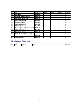
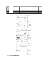
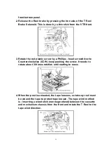
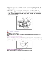
Page 9: ...45 46 47 48 49 50 5 3 Disassembly Method 9 ...

Page 10: ...1 2 Remove the 4 screws numbered 2 3 Slide the bottom panel and remove it 5 3 3 Removal of Upper Front Panel 1 Remove the 4 screws at right and left then draw the upper front panel 5 3 4 Removal of Front Panel 1 Remove the 4 screws at left and right Then draw it and remove the connector and remove the Front Panel 10 ...

Page 11: ... eject gear red counterclockwise until the screw which is used to fix the front loading u can be seen 2 Remove the 4 screws of the loading unit as shown below 5 3 6 Removal of Power Supply Unit 1 Remove 5 connectors with the Power Supply unit on the VTR bottom side 2 Remove 2 screws with the Power Supply unit on the VTR bottom side 11 ...

Page 12: ...supply unit 5 3 7 Removal of Mechanism Unit 1 Remove the front loading unit 2 Remove the connector P1 and P2 which are connected to mech interface at VTR bottom Remove the A C Head cable from the intermediate point and remove the P5003 and P5002 which are connected between the cylinder unit and Head Buffer board Then remove the 3 12 ...

Page 13: ...rews and Power 2 connector P14 then remove the fan motor 3 Remove 2 screws and mother board connector P32 then remove fan motor 5 4 Manual Tape Eject When a tape can not be ejected because of Power failure or mechanical tape damage remove the tape manually 1 Turns power off and remove the top panel and front upper and 13 ...

Page 14: ...rewdriver to Counterclockwise CCW keep pushing the screw It needs to rotate about 30 times rotation until starting to move 4 When the post is unloaded the tape loosens so take up reel must be wound the tape to protect tape loosen The tape wind method is inserting a wood stick non magnetized between the cassette and mechanism chassis from the front and rotate the T Reel to the tape wind direction 1...

Page 15: ...ing Procedures Note Turnspower off during cleaning Make sure the power isOFF before cleaning Use ethanol more than 99 purity ascleaning liquid 5 5 1 Cleaning of Head Chips Daily Clean heads by applying even pressure and rotating cylinder a few times Never wipe in up and down motion Never touch a cylinder by naked hand First wipe with a cloth soaked by cleaning liquid Then wipe with dry cloth 5 5 2...

Page 16: ...he Pinch Roller and Capstan with a cloth soaked by cleaning liquid 5 5 5 Cleaning of Post Weekly Wind a cloth on a pick Wipe each post dry with that pick Wipe again with a dry cloth For metal postswipe with cleaning liquid Then wipe dry again Note Use the clean cloth for cleaning purpose Do not use any dirty cloth 5 6 Mechanism Adjustment 5 6 1 Name of tape transportation 16 ...

Page 17: ...ff Tool VFK0357 Eccentric Driver 1 Turns power off 2 Close the pinch roller to the capstan shaft 3 Press the pinch solenoid by your hand and touch the pinch roller with the capstan shaft 4 Loosen the 2 screw A and adjust B portion so that the Gap T is in the specification by VFK0357 5 Tighten the 2 screw A after adjustment 17 ...

Page 18: ...W 4 Confirm the reel torque is in the specification when the brake is released and the reel starts rotation 5 Confirm T Reel torque in the same way with S Reel torque 6 Remove the Adaptor VKK1152 and attach the adaptor with the torque meter VFK1191 7 Attach the torque meter with the S Reel table and rotate it to B direction CCW 8 Confirm the reel torque is in the specification when the brake is re...

Page 19: ...4 as shown in the figure and adjust the post height 3 Adjust the S1 and T1 post height by VFK1149 and adjust T3 and T4 by VFK1151 Name Limit Post Driver S5 Post Note 1 VFK1149 S4 Post Note 1 VFK1149 T3 Post Lower Limit VFK1151 2 5mm Nut Box T4 Post Lower Limit VFK1151 2 5mm Nut Box Note Rotate CCW one turn from the lower limit 5 6 5 Tension ArmAdjustment Procedures 19 ...

Page 20: ...he voltage at TP201 is in the specification 2 If it is not adjust VR1 on the Mech I F Board so that the voltage is in the specification 5 6 7 Neutral Position Adjustment Board SERVO Specification 2 5 0 1V Test Point TP201 SERVO F1 Adjustment Tension Regulator Board Base Position Mode STOP M EQ Digital Volt Meter VFK1208 Black with a hole 1 Remove 4 screws on the Front Loading Unit and Remove it th...

Page 21: ... mode set the DIP SW1 at the rear panel ON to open the service menu Then select T REEL TRQ and press JOG SHTL key During adjustment JOG SHTL key must be hold Do not touch the adjustment drive to the Reel FG magnet 5 6 8 Tension ArmPLAY REV Voltage Confirmation and Adjustment Board SERVO Specification PLAY 3 8 0 05V REV 1 2 0 3V Test Point TP201 SERVO F1 Adjustment VR2 Mode STOP M EQ Digital Volt M...

Page 22: ...m Neutral Position Adjustment again If is out of specification after this adjustment replace the tension post unit 5 6 9 Tension Regulator Spring Adjustment Board SERVO Specification 11 1gf Test Point TP201 SERVO F1 Adjustment Tension Regulator Spring Hook B Mode STOP M EQ Digital Volt Meter VFK1188 30g Dial Tension Meter 1 Set the VTR in no tape loading 2 Press the tension post by the Dial Tensio...

Page 23: ... Tension Confirmation Board SERVO Specification 18 2gf Test Point TP201 Mode STOP M EQ Digital Volt meter VFK1188 30g Dial Tension Gauge 1 Place the VTR into no tape loading 2 Press the tension post by the Dial Tension Meter to R direction in STOP mode 3 Read the Dial Tension Meter when the voltage is 1 2 V REV position at TP201 and adjust the Tension Regulator Adjustment again 4 Grew the screw A ...

Page 24: ... VFK1145 Tension Meter 1 Playback the beginning of 63min M cassette 2 Set a tension meter between S3 and S4 post 3 Confirm the tension is in the specification 4 Set the VTR is in REV mode 5 Set the tension meter between S4 and S5 posts 6 Confirm the tension is in the specification Do not damage a tape during measurement 24 ...

Page 25: ...1PostHeight Mode PLAY ATF Tape VFM3580KM No 1 M EQ Oscilloscope Tool VFK1149 Post Driver 1 Playback the color bar portion of the alignment tape 2 Adjust S1 and T1 post height so that the R P envelope output is in the specification 3 When the S1 and T1 posts are adjusted first raise the post height and make small the entrance and exit side of the envelope then 25 ...

Page 26: ...he Tape edge All Post Limit Mode PLAY Tape Work Tape Tool VFK1149 Post Driver VFK1151 Nut Driver 1 Confirm the each Post Limit is as shown in figure if it is not adjust the post height 2 Confirm that there is no tape problem as D E F in the figure Post Limit Adjustment S5 Free or Lower Limit S5 Post Height S4 Lower Limit S4 Post Height S1 Upper Limit Linearity Coarse T1 Upper Limit Linearity Coars...

Page 27: ...n tighten the screw C and D 2 5 Kg cm Tilt G Adjust by tightening the screw except tilt and azimuth adjustment 1 0 Kg cm Height Fix H After the Height Adjustment tighten screw H to fix the A C Head Height Screw Tool A VFK1178 0 89 mm Nut Driver B VFK1150 5 5 mm Nut Driver F VFK1148 1 5 mm Nut Driver C D G VFK1209 Torque Driver VFK0912 1 5 mm Hex Driver Bit H VFK1190 1 5 mm L type Hex Wrench 1 Each...

Page 28: ...stment 5 6 16 A C Head Tilt Adjustment Specification No curling and bending at tape edge T3 Post Lower Limit Adjustment Screw A G A C Head Mode PLAY Tape Work Tape Tool VFK1148 VFK1178 Hex Wrench 1 Adjust A C Head Tilt by screw A so that the Tape is at lower limit at T3 Post 2 For this Adjustment loosen screw G and make tape curling at T3 lower flange then gradually tighten screw G to make the tap...

Page 29: ...justment Board SERVO Specification CTL Max C1 C2 1 8V or more Test Point TP30 SERVO F1 Adjustment Screw B H A C Head Mode PLAY Tape VFM3580KM No 1 M EQ Oscilloscope Tool VFK1150 Nut Driver VFK1190 Hex Wrench 1 Connect a scope to TP30 on Servo F1 board to observe CTL level 2 Confirm that CTL level is decreased when A C head is up and down at the point shown in the figure If the CTL level is increas...

Page 30: ...el is max 3 Tighten screw H with 2 0 Kg cm torque then confirm the CTL level again Reference 1 Confirm and adjust alternately this adjustment and A C Head each adjustment Azimuth and Height 5 6 18 A C Head Azimuth Adjustment 30 ...

Page 31: ...n screw G Reference Confirm and adjust alternately thisadjustment and A C Head each adjustment Azimuth and Height 5 6 19 A C Head Tilt Confirmation Specification A Amax 0 8 or more Test Point TP101 CUE H1 Adjustment Screw A G A C Head Mode PLAY Tape VFM3580KM No 1 M EQ Oscilloscope Tool VFK1178 VFK1148 Hex Wrench 1 Playback the alignment tape CUE audio 6 kHz portion 2 Confirm that screw G and H ar...

Page 32: ...djust screw A then tighten screw G with 1 0 Kg torque 5 It is necessary to complete the adjustment with screw A tighten and confirm that screw A is not loosen 6 If this is adjusted confirm the Play Limit Confirmation PLAY 5 6 20 A C Head Height Confirmation 32 ...

Page 33: ...to TP101 and raise the A C head or push down it to confirm the CTL level is not increased 3 If it is increased slightly adjust the A C Head Height Adjustment and confirm the CTL level is correct 4 If A C Head Height is changed the azimuth is changed also Therefore A C Head azimuth must be adjusted and confirm alternately 5 When A C Head Height is fixed tilt is changed by tightening screw H and the...

Page 34: ...5M Mode and playback an Alignment Tape A C Head H Position 2 Adjust Azimuth so that the CTL and CUE drop portion is match Refer to Azimuth Adjustment 3 Connect a scope CH1 to TP201 on H3 board and CH2 to TP722 on F1 board Then find the R P ENV lack portion and remember the H_SW is High or Low at the portion H_SW High or Low is changed at each tape loading 4 Adjust A C Head Horizontal Position so t...

Page 35: ...Post in REV Tape VFM3580KM No 1 Test Point TP30 SERVO F1 M EQ Oscilloscope Adjustment T4 Post Height Tool Nut Driver Mode REV X 1 1 Run the Tape in REV x 1 mode and confirm that the above specification is satisfied If it is not adjust the following items 2 Rotate the T4 nut 45 degrees each and confirm the specification and repeat this adjustment until the specification is satisfied 3 Specification...

Page 36: ...ERVO F1 Mode Self recording and playback Tape Work Tape M EQ Oscilloscope A C Head must be fixed 1 Set the VTR to 25M Mode and record a color bar signal and playback the just recorded portion Then observe the CTL 2 The CTL level is in the specifications in the following table CTL Output Level C1 C2 PLAY REV 1 REV 0 2 C1 C2 1 8V C1 C2 1 4V C1 C2 1 2V 1 If the PLAY Output Level is NG Then confirm th...

Page 37: ... S4 Tension Post NG NG OK NG NG NG S1 Post OK NG NG NG NG NG S1Post Envelope waveform Adj T1 Post OK NG NG NG NG NG T1Post Envelope waveform Adj T3 Post NG NG OK NG NG NG A C Head Tilt A C Head Tilt Adj T4 Post NG OK OK NG NG NG T4 Post Post Height Pre Adj 1 Playback a Tape and confirm the tape limit at each post is as shown in the above table 2 If it is not adjust each item according with the Adj...

Page 38: ...he same diamond style 2 Peak level V is always in the following specification V Vmax 0 9 3 If it is not confirm the S4 Post Height 5 6 26 Envelope Confirmation Test Point TP201 ENV RFEQ H3 Mode REW REV to PLAY Loading completion to PLAY FF to PLAY Tape L cassette 123 min pre recorded Tape begin M EQ Oscilloscope ThisAdjustment must be done after Envelope waveform Adjustment 38 ...

Page 39: ...pecification Confirm the Post Limit isasshown in the following table Mode REV Work Tape M Cassette MP Tape Tape begin and Tape end Post Tape Limit Refer to Figure A B C D E F S5 Post OK OK OK NG NG NG Tension Post NG OK OK NG NG NG S1 Post OK NG NG NG NG NG T1 Post OK OK OK NG NG NG T3 Post NG NG OK NG NG NG T4 Post NG NG OK NG NG NG 1 Run a tape in Reverse mode and confirm that the tape limit is ...

Page 40: ... NG NG NG Tension Post NG OK OK NG NG NG S1 Post OK NG NG NG NG NG T1 Post OK OK OK NG NG NG T3 Post OK OK OK NG NG NG T4 Post OK OK OK NG NG NG 1 Run a tape in FF REW mode and confirm that the tape limit is as shown in the above table 2 This confirmation is done after each adjustment 5 6 29 A C Head and T3 T4 Post Screw Grew A C Head Screw Grew Screw A Other Screw Grew amount About 3 mm About 5 m...

Page 41: ...T3 Post T4 Post Grew T3 Post T4 Post Grew amount About 3 mm About 5 mm 1 After A C Head Adjustment grew the Plastic Nut part of T3 and T4 posts 2 Remove the screw grew before Adjustment 5 6 30 LISTA 41 ...

Page 42: ...LISTA and copy the all files in the floppy disk of VFK1420 Type Lista50 exe in the DOS mode to run the LISTA software 4 Select the model of AJ D950 in the menu 5 Select a alignment tape to use LISTA Adjustment If it is not displayed choose one of the listed tape and type Y Y es or N o and resist the data which is supplied with the alignment tape 5 6 32 Alignment Tape Data Registration 1 Select 4 A...

Page 43: ...in the PC menu and displaysthe main menu 25M and 50m mode can be changed by 0 key 1 Set the VTR in Service Mode to open the service menu and select the item of A09 RP GAIN DP in the SERVO ADJUST menu 2 Playback a LISTA alignment tape VFM3581KM 3 Select the LISTA 6 ATF Error Signal Monitor and 1 2 Speed and type Enter to start the software 4 When the picture is appeared as shown in figure adjust AT...

Page 44: ...ication Linearity islessthan 3um Waving islessthan 1 5um Mode SERVO Adjustment Menu A10 RP LINEAR DP Test Point 1 ATF TP732 2 HSW TP722 RP HSW not TP723 PB HSW 3 GND TG510 Adjustment S1 and T1 Post Height Tape VFM3581KM or VFM3581KL 1 Open the Service Menu and select A10 RP LINEAR DP in the SERVO ADJUST 2 Playback a LISTA alignment Tape VFM3581KM 3 Select 2 Linearity Measurement then Linearity wav...

Page 45: ...yed on the monitor press SPACE key to hold the Peak 30 seconds 2 Press SHIFT and keys together and Waving value is displayed at left bottom of the monitor Then confirm the waving is 1 5 um or less and the waving is constant from the entrance to exit If the waving is out of specification adjust S1 Entrance and T1 Exit Post Height 3 After measurement press ESC key to return the main menu 5 6 36 PB H...

Page 46: ...tection 25M Mode Specification Sensitivity 150 15 mV um Mode Playback Test Point 1 ATF TP732 2 HSW TP723 PB HSW not TP722 RP HSW 3 GND TG510 Adjustment SERVO Adjustment Menu A09 RP GAIN P Tape VFM3581KM or VFM3581KL Before thisadjustment PB Head Sensitivity Adjustment 25M Mode must be completed 1 Open the Service Menu and select A11 PB GAIN DP 2 Playback a LISTA alignment tape VFM3581KM 3 Select L...

Page 47: ...splays the main menu 25M and 50m mode can be changed by 0 key 2 Set the VTR in Service Mode to open the service menu and select the item of A05 RP GAIN ED in the SERVO ADJUST menu 3 Playback a LISTA alignment tape VFM3581KM 4 Select the LISTA 6 ATF Error Signal Monitor and 1 2 Speed and type Enter to start the software 5 When the picture is appeared as shown in figure adjust ATF Gain so that the S...

Page 48: ...Sensitivity Measurement Finish and Sensitivity sensitivity value are appeared 5 6 40 LISTALinearity Confirmation and Waving Measurement 50M Mode Specification Linearity islessthan 3um Waving islessthan 1 5um Mode SERVO Adjustment Menu A06 RP LINEAR ED Test Point 1 ATF TP732 2 HSW TP722 RP HSW not TP723 PB HSW 3 GND TG510 Adjustment S1 and T1 Post Height Tape VFM3581KM or VFM3581KL 1 Open the Servi...

Page 49: ...the waving is out of specification adjust S1 Entrance and T1 Exit Post Height 3 After measurement press ESC key to return the main menu 5 6 41 PB Head LISTASensitivity Adjustment 50M Mode Specification Sensitivity 150 15 mV um Mode SERVO Adjustment Menu A07 PB GAIN ED Test Point 1 ATF TP732 2 HSW TP723 PB HSW not TP722 RP HSW 3 GND TG510 Adjustment SERVO Adjustment Menu A07 PB GAIN ED Tape VFM3581...

Page 50: ...sadjustment PB Head Sensitivity Adjustment 50M Mode must be completed 1 Open the Service Menu and select A07 PB GAIN ED 2 Playback a LISTA alignment tape VFM3581KM 3 Select LISTA Main Menu 1 Sensitivity Measurement Press enter when 1 2 Speed is appeared to start the Sensitivity measurement 4 Confirm that the specification is satisfied when Sensitivity Measurement Finish and Sensitivity sensitivity...

Page 51: ...t 2 Use the correct tool in the Jigs and Tools list 3 After replacement clean the VTR according with the cleaning procedures 5 7 1 Cylinder Unit Replacement Removal of Cylinder Unit 1 Remove the T1 guide and cleaning arm unit Refer to the cleaning arm unit replacement 2 Remove 2 connectors P5002 P5003 on the Head Buffer board and remove the screw on the flexible cable Note Be careful to remove the...

Page 52: ...ithout touching any parts Note Do not touch the cylinder surface by finger directly Installation of cylinder 1 Install a Cylinder unit as reverse order of its removal Note Set the Mechanical Chassis pins are matched with the specified cylinder holes on the bottom of the cylinder 2 After T1 Guide installation T1 Guide Position Adjustment is 52 ...

Page 53: ...all a Cleaning Arm Unit to the T2 Arm Unit Then remove the spring from the cleaner base plate and hook to cleaning arm unit Push the cleaning arm unit into T2 Arm Unit 2 Push the Cleaner Solenoid Rotate the cylinder and confirm that the cleaner roller is rotated by the cylinder movement 3 Install a T1 Guide 4 After T1 Guide installation T1 Guide position adjustment is necessary 5 7 3 T1 Guide Posi...

Page 54: ...de by moving arrow direction B 5 7 4 Adjustments after Cylinder Unit Replacement 1 Adjust following items after cylinder unit replacement Note For the PG Shifter Adjustment release hand from the search button after changing the PG Shifter value at right of PG SHIFT on the monitor If the value isnot changed for a long time tape error or ITI envelope lack may be occurred 5 7 5 A C Head Replacement R...

Page 55: ...the height adjustment spring a Remove the A C Head Unit Note Remember the Nut C height before removing it 3 Remove 2 screws A and remove P1 on AC HEAD I F board and P2030 on Mech I F board then remove A C Head 4 Remove 2 screws D and remove the shield case 5 Unsolder the Lead wire from the A C Head When unsolder the lead wires do not unsolder all at the same time 55 ...

Page 56: ...ll the shield case 3 Install the A C head to the A C head plate by 2 screws A Then set to parallel the gap between A C Head and A C Head Plate 4 Install the A C Head unit 5 Hang on the Head Height Adjustment Spring and tighten the Nut C 6 Clean the surface of the A C Head 7 A C Head Adjustment is necessary 56 ...

Page 57: ... 7 6 A C Head Adjustment 1 After A C Head Replacement from the item of A C Head Tilt to the item of A C head horizontal position adjustment are necessary Note Keep loosen the hex screw B at the side of A C head until A C head height adjustment completion 2 A C Head Adjustment and Confirmation are shown in the following flow chart 57 ...

Page 58: ...T brake solenoid iron core are released 7 Push the M Stopper Solenoid to release the M Stopper 8 Remove 4 Screws C D and E 9 The Reel Table is hooked with inner rail Slightly lift the Reel Table so that it does not touch the brake release arm Then remove the Reel Table Note Memorize the groove position of Reel Base which isinserted the pin of Drive Arm Unit The position can remember by the attache...

Page 59: ...the iron core of M stopper solenoid 5 Unload completely by rotating the Red Plastic screw CCW 6 Insert the flexible cable into P34 and P35 on the Mech I F board 7 Confirm the Main Brake Torque Refer to the Main Brake Torque Confirmation 8 Adjust the Motor Torque Offset Refer to the Motor Torque Offset Adjustment 9 Confirm the Tension Value Refer to the Tension Confirmation Mech IF Board Removal Re...

Page 60: ...pply and take up brake arm unit Installation of Brake Arm Unit 1 Install new supply and take up brake arm units as reverse order of removal Note Hook the brake arm spring at the position shown in the figure 2 After the Brake Arm Unit Installation confirm the Main Brake Torque Refer to the Main Brake Torque Confirmation Reel Brake Arm Unit Replacement 5 7 9 Supply Brake Solenoid Replacement and Adj...

Page 61: ...erse order of its removal Note Set the supply brake spring at the position shown in the figure 2 After installation adjust following procedures Adjustment Procedures 1 Set the Reel Table at M cassette position 2 Confirm the gap A between Brake pad and Turn table is 0 2 mm to 0 5 mm 3 If the gap A is out of specification loosen 2 screws and adjust brake solenoid unit as arrow direction so that the ...

Page 62: ...panel 4 Remove the connector P18 on the Mech Interconnection board 5 Remove 2 screws A and remove the take up brake solenoid base unit 6 Remove 2 screws B and remove the Brake Solenoid from the Take up Brake Solenoid Base Unit Take up Brake Solenoid Removal Installation 1 Install a new Take up Brake Solenoid as reverse order of its removal Note Install a take up brake spring as shown in the figure...

Page 63: ...move 2 screws A and remove the Pinch Solenoid Unit 5 Remove 2 screws B and remove the Pinch Solenoid Angle 6 Remove 2 screws C and remove pinch solenoid base then remove Pinch Solenoid Installation of Pinch Solenoid 1 Install a new Pinch Solenoid as reverse order of its removal After installation Pinch Solenoid Position Adjustment is necessary Refer to Pinch Solenoid Position Adjustment Pinch Sole...

Page 64: ...her C and remove the Pinch Arm Unit Installation of Pinch Arm Unit 1 Install a new Pinch Solenoid as reverse order of its removal After installation adjust Pinch Solenoid Position Adjustment Refer to Pinch Solenoid Position Adjustment Pinch Arm Unit Replacement 5 7 13 Loading Motor Replacement Removal of Loading Motor 1 Remove the top panel 2 Remove the front loading unit 3 Remove the bottom panel...

Page 65: ...Install the Loading Motor unit with 2 screws C For this installation be careful that the pin of Mode SW unit should be matched to groove position of main Cam Gear 3 Install the emergency shaft with screw B 4 Install the Pinch Solenoid Unit After installation adjust Pinch Solenoid Position Adjustment Refer to Pinch Solenoid Position Adjustment 5 Connect the connector P21 Removal of Loading Motor 5 ...

Page 66: ...e Main Cam Gear 2 After Pinch Solenoid Unit adjust Pinch Solenoid Position Adjustment Refer to Pinch Solenoid Position Adjustment Removal of Mode Switch Unit 5 7 15 Main Cam Gear Replacement Removal of Main Cam Gear 1 Remove the top panel 2 Remove the front loading unit 3 Remove the Pinch Solenoid Unit and Loading Motor Neutral Unit Refer to Loading Motor Replacement and Pinch Arm Unit Replacement...

Page 67: ...l 2 Remove the front loading unit 3 Remove the screw A and remove the S5 Post Base Unit Installation of S5 Base Unit 1 Install the new S5 Post Base Unit as reverse order of its removal Note Install the S5 Post by the position fix as shown in the figure 2 After installation Post Pre adjustment and Linearity adjustment are necessary 67 ...

Page 68: ...unit 3 Remove the cut washer A and remove the tension regulator spring from its hook then remove the tension arm unit Installation of Tension Arm Unit 1 Install the new Tension Arm Unit as reverse order of its removal 2 After installation adjust tension arm adjustment following the tension arm adjustment flow chart Removal of Tension Arm Unit 68 ...

Page 69: ...t 5 Remove the screw A and remove the S1 Post from the loading rail 6 Remove the E ring A and remove the S1 Loading Arm Unit Installation of S1 Post Loading Arm Unit 1 Install a new S1 Post Loading Arm Unit as reverse order of removal After its installation S1 Post Loading Arm Unit Phase Adjustment is necessary 2 After its installation confirm the S1 Post moves smoothly on the loading rail Then Ad...

Page 70: ...oves on the Loading Rail Then Linearity Adjustment is necessary 5 7 20 T1 Loading ArmUnit Replacement and Adjustment Removal of T1 Loading Arm Unit 1 Remove the top panel 2 Remove the front loading unit 3 Remove the cylinder unit Refer to the cylinder unit replacement 4 Rotate the emergency eject shaft CW to load the T1 Post and make a space to remove the screw D as shown in Fig 6 15 1 5 Remove th...

Page 71: ...t is necessary T1 Loading Arm Unit Position Adjustment 5 7 21 Cleaner Solenoid Replacement and Adjustment Removal of Cleaner Solenoid 1 Remove the top panel 2 Remove the Front Loading Unit 3 Remove the connector P11 on the Mechanical Interconnection Board 4 Remove two screws A and remove the Cleaner Solenoid Unit 5 Remove two screws B and remove the Cleaner Solenoid Installation of Cleaner Solenoi...

Page 72: ...s out of specification loosen 2 screws A and move the cleaner solenoid arrow C direction and adjust the clearance D is in the specification 3 Push the cleaner solenoid shaft and confirm that the cleaner roller touches the cylinder Then confirm that the cleaner roller returns original position when the shaft is released 4 Push the Solenoid shaft and rotate the cylinder and confirm that the cleaner ...

Page 73: ...er Position Adjustment isnecessary 5 7 23 Cleaner Roller Position Adjustment Tool Eccentric Driver VFK0357 1 Confirm that the clearance A between cylinder unit and cleaner roller is 1 0 mm to 1 2 mm 2 If it is out of specification loosen screw B and move the cleaner base unit and adjust its position by the eccentric driver 73 ...

Page 74: ...Stopper Solenoid Installation of M Stopper Solenoid 1 Install a new M Stopper Solenoid as reverse order of its removal 2 After its installation following adjustment is necessary M Stopper Solenoid Removal Adjustment Procedures 1 Set the Reel Table at L cassette position 2 Release the M Stopper by pushing the M Stopper Solenoid Shaft 3 Loosen the screw A and adjust the M Stopper Solenoid Unit Posit...

Page 75: ...4 Remove the connector P17 on the Mech Interconnection board 5 Remove the MIC Drive REV Spring 6 Remove 3 screws and remove the MIC Rail Unit Installation of MIC Rail Unit 1 Install a new MIC Rail Unit as reverse order of its installation 2 Confirm that M and L cassette touches MIC Rail Unit MIC Rail Unit Removal 5 7 26 Reel Drive Motor Unit Replacement Removal of Reel Drive Motor Unit 1 Remove th...

Page 76: ...r Unit as reverse order of its removal Reel Drive Motor Unit Removal 5 7 27 L M Brake Release U Replacement Installation of L M Brake Release Unit 1 Remove the top panel 2 Remove the front loading unit 3 Remove the screw A and remove the L M Brake Release Unit Installation of L M Brake Release Unit 1 Install a new L M Brake Release Unit as reverse order of its removal L M Brake Release Unit Remova...

Page 77: ...r C and remove the MIC intermittent gear 8 Remove the cut washer D and remove the Reel Drive Arm Unit 9 Remove the supply and take up reel rotor unit Refer to Supply and Take up Reel Table Unit Replacement 10 Remove the cut washer E and remove the supply and take up side base drive arm unit 11 Remove the cut washer F and remove the slide load Slide Rod Unit Removal Reel Drive Arm Unit Removal Inst...

Page 78: ...le 6 Install 3 cut washers A B and C Adjustment Note 1 Close the Reel Table to M Cassette position 2 Set the MIC SW Distinction SW to the nearest position from the Reel 3 MIC Drive Arm Unit Pin position is as shown in the above figure 4 Reel Drive Came Gear Hole and MIC Intermittent Gear phase are matched 5 7 29 T4 Post Position Adjustment 1 Set the VTR unloading condition 2 Confirm the T4 post ho...

Page 79: ...06 as shown in the figure and set the capstan housing 3 While rotating the capstan shaft CCW tighten the thrust screw CW slowly and stop it when the rotation becomes smoothly 4 Rotate another 180 degrees or 270 degrees from the stop position of item 3 5 Grew the thrust screw 6 Confirm the oil seal as shown in figure 79 ...

Page 80: ...he front panel and confirm that the Service Menu is displayed on the TV monitor Video Out 3 4 Rotate the search dial and select the item 5 While holding down the search button rotate the search dial to change the adjustment data 6 The adjustment data is changed 6 1 2 Displaying the Error Rate The Error Rate isdisplayed on the Audio Meter in the Service Mode 1 Place the unit in the Service Mode 2 S...

Page 81: ...L_TRQ by the JOG DIAL 5 Set a torque meter at T Reel table and adjust the torque data so that the torque is in the specification by JOG DIAL while pressing JOG SHTL key 6 Measure it 5 times and calculate the average and adjust the torque data so that the average is in the specification 7 Set the marker at S_REEL_TRQ by JOG DIAL 8 Set a torque meter at S Reel table and adjust the torque data so tha...

Page 82: ...ght of PG SHIFT ED is renewed 4 Connect a scope to TP722 andTP729 5 Confirm the t1 and t2 are 126 8us 2us 6 2 3 PG Shifter Adjustment 2 BOARD SERVO F1 SPEC t1 t2 253 6 s 4 s TEST RP_L_HSW TP722 SPA_REC TP729 ADJUST INPUT VIDEO OUT 3 MODE PLAY TAPE VFM3580KM M EQ Oscilloscope 1 Open the Service menu and select PG SHIFT DP 2 Playback the color bar portion of the alignment tape 3 Press search button ...

Page 83: ...R FREQ ADJ 525 Board V_OUT F6 Specification 0Vdc 0 1V Test Point TP13 B 1 Adjustment Point VC1 B 1 Input Signal REF IN BB NTSC Mode EE INT SG Tape M EQ Oscilloscope 1 Place the unit in the 525 mode 2 Adjust VC1 so that the DC level is 0V 0 1V DC 6 3 2 4fsc PLL CENTER FREQ ADJ 625 83 ...

Page 84: ...1 so that the DC level is 0V 0 1V DC 6 3 3 Burst Sample Phase Adj 525 Board V_OUT F6 Specification Test Point TP8 A 4 TP10 B 4 Adjustment Point S H PLS P VR6 A 3 Input Signal REF IN BB NTSC Mode EE INT SG Tape M EQ Oscilloscope 1 Place the unit in the 525 mode 2 Adjust VR6 so that the sample pulse is located at center of the burst signal as shown in figure 6 3 4 Burst Sample Phase Adj 625 84 ...

Page 85: ...center of the burst signal as shown in figure 6 3 5 CF PHASE ADJUSTMENT 1 525 Board V_OUT F6 Specification Test Point TP4 A 2 SG CF OUT Adjustment Point CF ADJ N VR7 B 3 Input Signal REF IN BB NTSC Mode EE INT SG Tape M EQ Oscilloscope 1 Place the unit in the 525 mode 2 Scope CH1 SG CF CH2 TP4 TRIG SG CF falling edge 3 Rotate the VR7 fully CCW 4 Rotate the VR7 CW slowly 5 Set the VR7 so that the w...

Page 86: ...ustment Point CF ADJ N VR7 B 3 Input Signal REF IN BB NTSC Mode EE INT SG Tape M EQ Oscilloscope 1 Place the unit in the 525 mode 2 Adjust VR7 so that the rising edge of the TP2 is at center of the data period as shown in figure 3 After adjustment confirm that CF phase refer to the item CF PHASE ADJUSTMENT 1 525 6 3 7 CF PHASE ADJUSTMENT 1 625 86 ...

Page 87: ...13 to CW slowly 5 Set the VR13 so that the waveform phases are same as shown in figure The CF waveform isdifferent by SG type 6 3 8 CF PHASE ADJUSTMENT 2 625 Board V_OUT F6 Specification Test Point TP1 B 1 TP2 B 1 Adjustment Point CF ADJ P VR13 A 3 Input Signal REF IN BB PAL Mode EE INT SG Tape M EQ Oscilloscope 1 Place the unit in the 625 mode 2 Adjust VR13 so that the pulse TP2 is at center of t...

Page 88: ...C Mode EE INT SG Tape M EQ Oscilloscope WFM VSC 1 Place the unit in the 525 mode 2 SYSTEM MENU SETTING SYS H 0 SYS SC 0 3 WFM VSC MODE VSC REF EXT mode INPUT CHA 4 Set the CHA Burst Phase to 0 5 Change the INPUT SELECT to CHB 6 Adjust VR15 so that the Burst Phase is 0 7 WFM VSC MODE WFM REF EXT mode INPUT CHB 8 Adjust VR14 so that the H Sync Phase as close as the CHA H Sync Phase 88 ...

Page 89: ...ope WFM VSC 1 Place the unit in the 625 mode 2 SYSTEM MENU SETTING SYS H 0 SYS SC 0 3 WFM VSC MODE VSC REF EXT mode INPUT CHA 4 Set the CHA Burst Phase to 0 5 Change the INPUT SELECT to CHB 6 Adjust VR16 so that the Burst Phase is 0 7 WFM VSC MODE WFM REF EXT mode INPUT CHB 8 Adjust VR4 so that the H Sync Phase as close as the CHA H Sync Phase 9 After adjustment turn POWER switch ON and OFF and co...

Page 90: ...he character black level is at the Pedestal level 6 3 12 COMPOSITE OUT LEVEL ADJ Board V_OUT F6 Specification 1V 20mV Test Point VIDEO OUT 1 Adjustment Point VR2 I 1 Input Signal Mode EE INT SG Tape M EQ WFM Note Do not use an extension board 1 Adjust VR2 so that the VIDEO OUT level is in the specification 6 4 Audio AD_DA 6 4 1 SW Setting 90 ...

Page 91: ... HIGH SW141 HIGH 6 4 2 M EQ Setting Board Specification Test Point Adjustment Point Input Signal Mode Tape M EQ Audio Analyzer Audio Precision 1 GENERATOR OUTPUT A B BAL 50 FLOAT ANALYZER CHANNEL A INPUT 100K CHANNEL B INPUT 100K 6 4 3 MENU Setting Board Specification Test Point Adjustment Point Service MENU User MENU Input Signal Mode EE Tape M EQ Monitor Service Menu Setting 91 ...

Page 92: ... LV 0dB 706 CH1 OUT LV 0dB 707 CH2 OUT LV 0dB 708 CH3 OUT LV 0dB 709 CH4 OUT LV 0dB 711 MONIL OUT LV 0dB 712 MONIR OUT LV 0dB 713 MONI OUT VAR 714 EMPHASIS OFF 722 REC CH1 CH1 723 REC CH2 CH2 724 REC CH3 CH3 725 REC CH4 CH4 6 4 4 Output Balance Adjustment Board A_ADDA F8 Specification Waveform Level Minimum Test Point AUDIO OUT CH1 CH4 MONI OUT LCH RCH Adjustment Point VR402 CH1 VR477 CH2 VR522 CH...

Page 93: ...ication 0dBu 0 2dB Test Point AUDIO OUT CH1 CH4 MONI OUT LCH RCH Adjustment Point VR401 CH1 VR476 CH2 VR551 CH3 VR626 CH4 VR702 LCH VR701 RCH Input Signal INT SG Mode EE Tape M EQ Oscilloscope Audio Analyzer Audio Precision 1 User menu Setting AUDIO MENU 700 INT SG ON 713MONI OUT UNITY 2 Adjust VR401 so that the CH1 level is 0dBu 0 2dB 3 Repeat the adjustment in the same way about the other Audio ...

Page 94: ...erminal of CH1 3 Adjust VR1 so that the CH1 output level is minimum 4 Repeat an adjustment in the same way about the other Audio channels CMMR Common Mode Reduction Ratio CMTST Common Mode Test 6 4 7 Input level Adjustment Board A_ADDA F8 Specification 0dBu 0 2dB Test Point AUDIO OUT CH1 CH2 CH3 CH4 Adjustment Point VR2 CH1 VR42 CH2 VR102 CH3 VR142 CH4 Input Signal AUDIO IN CH1 CH2 CH3 CH4 Sinewav...

Page 95: ... VR to UNITY 2 Set the switches on the CUE P C Board as shown below 3 Service Menu G00 AUDIO ADJUST G01 REF LEVEL FS 20 4 Audio analyzer Setting Output Impedance Lessthan 50 BAL Input Impedance More than 100K BAL BAL Balance 6 5 2 CTL Erase CUE Erase Current ADJ Board CUE H1 Specification More than 240mVp p Test Point TP4202 TP4203 Adjustment Point T4203 T4204 Input Signal Mode REC PLAY Tape REC P...

Page 96: ...cification 6 5 3 CUE Bias Current adjustment Board CUE H1 Specification 7mVrms 0 5mVrms Test Point TP4002 GND TP4003 Adjustment Point T4202 VR4202 Input Signal Mode REC PLAY Tape REC PB Tape M EQ Electric Volt Meter 1 Connect a Volt Meter between TP4002 and TP4003 GND and confirm that the voltage is in the specification 2 If it is out of Specification adjust T4202 so that the level becomes maximum...

Page 97: ... Cancel Adjustment Board CUE H1 Specification 50M mode Lessthan 40dBu 25M mode Lessthan 35dBu Test Point CUE OUT Adjustment Point VR4006 VR4003 50M VR4007 VR4004 25M Input Signal Mode PLAY Tape No signal recorded Tape M EQ Audio Analyzer Audio precision 50M Mode 1 Analyzer setting Input BPF 600Hz 2 Place the unit in the 50M mode 3 Confirm that the CUE OUT Level noise level is in the specification ...

Page 98: ...Audio Analyzer Audio precision 1 Place the unit in the 50M mode 2 Supply a 1kHz 0dBu signal into the CUE IN and Record the input signal for a few minutes 3 During the recording mode slightly adjust VR4001 4 Playback the just recorded portion and confirm that the CUE OUT level is in the specification 5 If it is not repeat step 3 4 6 Place the unit in the 25M mode 7 Supply a 1kHz 0dBu signal into th...

Page 99: ...ed portion and confirm the 300Hz through 6KHz signal are within 3dB compared with 1kHz level 4 If it is out of specification adjust SW4001 1 2 3 4 position so that the frequency characteristic is in the specification SW4001 3 4 1Khz 6Khz SW4001 1 2 6Khz 6 6 RF EQ 6 6 1 ENV Level Adjustment Lch Board RF EQ H3 Specification Vdc 2 5V 0 2V Test Point TP1 TP2 TP103 TP203 Adjustment Point Service Menu I...

Page 100: ...Main Menu 8 Select the item E00 RF DP 9 Adjust E23 PB MAG L1 and E24 PB MAG L2 so that the DC level Vdc is 2 5V 0 2V 10 Change the connection of the Oscilloscope CH1 TP203 CH2 TP1 Trigger 11 Adjust E15 RP MAG L1 and E16 RP MAG L2 so that the DC level Vdc is 2 5V 0 2V 12 Eject a tape and close the Service Menu 13 Turns power OFF 6 6 2 ENV Level Adjustment Rch Board RF EQ H4 Specification Vdc 2 5V 0...

Page 101: ...5V 0 2V 7 Press the MENU Button and the return to the Service Main Menu 8 Select the item E00 RF DP 9 Adjust E27 PB MAG R1 and E28 PB MAG R2 so that the DC level Vdc is 2 5V 0 2V 10 Change the connection of the Oscilloscope CH1 TP203 CH2 TP1 Trigger 11 Adjust E19 RP MAG R1 and E20 RP MAG R2 so that the DC level Vdc is 2 5V 0 2V 12 Eject a tape and close the Service Menu 13 Turns power OFF 6 6 3 Pr...

Page 102: ...ervice Menu Input Signal Mode Playback Tape VFM3580KM Color Bar Portion M EQ Oscilloscope 1 Open the service Menu and select item B00 EQ ED ADJUST Menu 2 Measure the voltage at TP603 in the Eject mode V eject 3 Playback a 25M Master Tape A picture is not appeared on the monitor 4 Set the items in the Service MENU as follows B01 PB PLL PHS L 10 B02 PB PLL SL L 60 B41 VITERBI MODE OFF B42 PB MODE PB...

Page 103: ... Service Menu as follows B15 RP PLL PHS L 45 B16 RP PLL SL L 60 B42 PB MODE RP H 4 Measure the Voltage at TP503 V play 5 Adjust B32 RP PLL VCO L so that the voltage is in the specification 6 Confirm the red segment is not displayed on the Error meter of L1 and L2 7 If it is not adjust B15 RP PLL PHS L and B16 RP PLL SL L and return to the step 5 6 6 6 PLL Lock Confirmation 25M Mode PB Lch Board RF...

Page 104: ...Error meter of L1 and L2 7 If it is not adjust D01 PB PLL PHS L and D02 PB PLL SL L and return to the step 5 6 6 7 PLL Lock Confirmation 25M Mode RP Lch Board RF EQ H3 Specification V play V eject 0 05V Test Point TP505 Adjustment Point Service Menu Input Signal Mode Playback Tape VFM3580KM Color Bar Portion M EQ Oscilloscope 1 Measure the voltage at TP505 in the Eject mode V eject 2 Playback a 25...

Page 105: ...Color Bar Portion M EQ Oscilloscope 1 Measure the voltage at TP603 in the Eject mode V eject 2 Playback a 25M Master Tape Note A normal picture is not appeared on the monitor 3 Set the items in the Service Menu as follows B08 PB PLL PHS R 10 B69 PB PLL SL R 60 B41 VITERBI MODE OFF B42 PB MODE PB H 4 Measure the Voltage at TP603 V play 5 Adjust B35 PB PLL VCO R so that the voltage is in the specifi...

Page 106: ...B23 RP PLL SL R 60 B42 PB MODE PB H 4 Measure the Voltage at TP503 V play 5 Adjust B36 RP PLL VCO R so that the voltage is in the specification 6 Confirm the red segment is not displayed on the Error meter of R1 and R2 7 If it is not adjust B22 RP PLL PHS R and B23 RP PLL SL R and return to the step 5 6 6 10 PLL Lock Confirmation 25M Mode PB Rch Board RF EQ H4 Specification V play V eject 0 05V Te...

Page 107: ...PHS R and D09 PB PLL SL R and return to the step 5 6 6 11 PLL Lock Confirmation 25M Mode RP Rch Board RF EQ H4 Specification V play V eject 0 05V Test Point TP505 Adjustment Point Service Menu Input Signal Mode Playback Tape VFM3580KM Color Bar Portion M EQ Oscilloscope 1 Measure the voltage at TP505 in the Eject mode V eject 2 Playback a 25M Master Tape Note A normal picture is not appeared on th...

Page 108: ...3 Playback a 25M Master Tape 4 Adjust B37 ADC LEVEL L so that the noise level is minimized as shown in the following figure 5 Change the connection of scope CH1 to the TP2 H2 from TP1 H2 6 Adjust B38 ADC LEVEL R so that the noise level is minimized as shown in the following figure 7 Escape the EQ ED ADJUST Menu and select the D00 EQ DP ADJUST Menu 8 Adjust D38 ADC LEVEL R so that the noise level i...

Page 109: ...e menu and select item B00 EQ ED ADJUST menu 2 Playback a 25M Master Tape 3 Set the item as follows B41 VITERBI MODE OFF 4 Adjust each adjustment item so that the L1 and L2 error rate is minimum Adjustment items procedures A B01 PB PLL PHS L B02 PB PLL SL L B B29 PB MAIN DL L C B03 PB AEQ L D B04 PB GAIN L1 B05 PB PHASE L1 E B06 PB GAIN L2 B07 PB PHASE L2 6 6 14 EQ Adjustment 50M PB Rch 109 ...

Page 110: ...error rate is minimum Adjustment items procedures A B08 PB PLL PHS R B09 PB PLL SL R B B33 PB MAIN DL R C B10 PB AEQ R D B11 PB GAIN R1 B12 PB PHASE R1 E B13 PB GAIN R2 B14 PB PHASE R2 6 6 15 EQ Adjustment 50M PB VITERBI ON Board RF EQ Specification Test Point Error Meter Adjustment Point Service Menu Input Signal Mode Playback Tape VFM3580KM Color Bar Portion M EQ Oscilloscope 1 Set the items as ...

Page 111: ...enu Input Signal Mode Playback Tape VFM3580KM Color Bar Portion M EQ 1 Playback the 25M Master Tape 2 Set the item as follows B42 PB MODE RP H 3 Adjust B15 RP PLL PHS L and B16 RP PLL SL L so that the L1 and L2 error rate is minimum 4 Adjust B30 RP MAIN DL L so that the L1 and L2 error rate is minimum 5 Adjust B17 RP AEQ L so that the L1 and L2 error rate is minimum 6 Adjust B18 RP GAIN L1 and B19...

Page 112: ... is minimum 5 Adjust B24 RP AEQ R so that the R1 and R2 error rate is minimum 6 Adjust B25 RP GAIN R1 and B26 RP PHASE R1 so that the R1 error rate is minimum 7 Adjust B27 RP GAIN R2 and B28 RP PHASE R2 so that the R2 error rate is minimum 8 Adjust B22 RP PLL PHS R and B23 RP PLL SL R so that the R1 and R2 error rate is minimum 6 6 18 Setting For 25M EQ Adjustment Board RF EQ Specification Test Po...

Page 113: ...LL SL L so that the L1 and L2 error rate is minimum 4 Adjust D29 PB MAIN DL L so that the L1 and L2 error rate is minimum 5 Adjust D03 PB AEQ L so that the L1 and L2 error rate is minimum 6 Adjust D04 PB GAIN L1 and D05 PB PHASE L1 so that the L1 error rate is minimum 7 Adjust B06 PB GAIN L2 and B07 PB PHASE L2 so that the L2 error rate is minimum 6 6 20 EQ Adjustment 25M PB Rch Board RF EQ Specif...

Page 114: ... D14 PB PHASE R2 so that the R2 error rate is minimum 6 6 21 EQ Phase Adjustment 25M PB Board RF EQ Specification Test Point Adjustment Point Service Menu Input Signal Mode PLAY Tape VFM3580KM Color Bar Portion M EQ 1 Playback the 25M Master Tape 2 Set the item as follows D41 VITERBI MODE OFF 3 Adjust D05 PB PHASE L1 so that the L1 error rate is minimum 4 Adjust D07 PB PHASE L2 so that the L2 erro...

Page 115: ...Input Signal Mode PLAY Tape VFM3580KM Color Bar Portion M EQ 1 Playback the 25M Master Tape 2 Set the item as follows D42 PB MODE RP H 3 Adjust D15 RP PLL PHS L and D16 RP PLL SL L so that the L1 and L2 error rate is minimum 4 Adjust D30 RP MAIN DL L so that the L1 and L2 error rate is minimum 5 Adjust D17 RP AEQ L so that the L1 and L2 error rate is minimum 6 Adjust D18 RP GAIN L1 and D19 RP PHAS...

Page 116: ... H 3 Adjust D22 RP PLL PHS R and D23 RP PLL SL R so that the R1 and R2 error rate is minimum 4 Adjust D34 RP MAIN DL R so that the R1 and R2 error rate is minimum 5 Adjust D24 RP AEQ L so that the R1 and R2 error rate is minimum 6 Adjust D25 RP GAIN R1 and D26 RP PHASE R1 so that the R1 error rate is minimum 7 Adjust D27 RP GAIN R2 and D28 RP PHASE R2 so that the R2 error rate is minimum 8 Adjust ...

Page 117: ...P PHASE R2 so that the R2 error rate is minimum 6 6 26 ADC Level Fine Adjustment Board X CAN H2 Specification Test Point TP1 TP2 H2 TP2 H3 Adjustment Point Service Menu Input Signal Mode PLAY Tape VFM3580KM Color Bar Portion M EQ Oscilloscope 1 Connect a scope CH1 to TP1 on H2 X CAN Board and CH2 to TP2 on H3 RF EQ L Board Scope CH1 TP1 H2 CH2 TP2 H3 2 Open the Service Menu and select the item B00...

Page 118: ... 10 Adjust D37 ADC LEVEL L so that the noise level is minimized as shown in the following figure Note Confirm that the DC level isnot held around 2 5V 6 6 27 Error Rate Confirmation 50M Board RF EQ Specification Test Point Adjustment Point Service Menu Input Signal Mode PLAY Tape VFM3580KM Color Bar Portion M EQ 1 Set the items in the USER MENU as follows 012 SYS FORMAT 422 013 PB FORMAT MANUAL 2 ...

Page 119: ...aster Tape and playback a 50M color bar Tape 11 Confirm that the color bar is displayed on the monitor 6 6 28 Error Rate Confirmation 25M Board RF EQ Specification Test Point Adjustment Point Service Menu Input Signal Mode PLAY Tape VFM3580KM Color Bar Portion M EQ 1 Set the items in the USER MENU as follows 012 SYS FORMAT 411 013 PB FORMAT MANUAL 2 Open the Service Menu and select item D00 EQ DP ...

Page 120: ...O Error 7 Set the item as follows B42 PB MODE RP H 8 Measure each error rate about L1 L2 R1 R2 VIDEO AUDIO 9 Confirm that the error rate is less than 14 segments on the error meter 6 6 29 REC Current and Frequency Characteristic Adjustment 1 Spectrum Analyzer setting 120 ...

Page 121: ...he USER MENU as follows 012 SYS FORMAT 422 013 PB FORMAT MANUAL 000 INT SIG CB 4 Open the Service Menu 6 6 30 REC Current and Frequency Characteristic Adjustment 50M Lch Board RF EQ H3 Specification Test Point TP104 TG101 TP2 TG1 Adjustment Point Service Menu Input Signal INT SG Color bar Mode REC Tape REC PB Tape M EQ Spectrum Analyzer 1 Connect a Spectrum Analyzer to the TP104 H3 EXT TRIG TP2 H3...

Page 122: ...ximum 7 Store the signal in the TRACE B 8 Adjust following items so that the waveform becomes TRACE A of the following figure Adjustment items C01 REC CURR L1 C03 REC CURR L2 C02 REC FREQ L1 C04 REC FREQ L2 9 Add 110 to the value of C01 REC CURR L1 and C03 REC CURR L2 Ex In case of 50 60 10 After adjustment compare the spectrum of Master Playback and Confidence Playback 6 6 31 Comparison Of the Sp...

Page 123: ...ACE B Level 2 0 dB 6 6 32 REC Current and Frequency Characteristic Adjustment 50M Rch Board RF EQ H4 Specification Test Point TP104 TG101 TP2 TG1 Adjustment Point Input Signal INT SG Color bar Mode REC Tape RP PB Tape M EQ Spectrum Analyzer 1 Connect a Spectrum Analyzer to the TP104 H4 EXT TRIG TP2 H4 RECALL REG 1 GND TG101 2 Insert a R P Tape and record a color bar signal 3 Select the item C00 RF...

Page 124: ...RR R2 C08 REC FREQ R1 C10 REC FREQ R2 9 Add 110 to the value of C07 REC CURR R1 and C09 REC CURR R2 Ex In case of 50 60 10 After adjustment compare the spectrum of Master Playback and Confidence Playback 6 6 33 Comparison Of the Spectrum of Master PB and Confidence PB 50M Rch Board RF EQ H4 Specification Test Point TP104 TG101 TP2 TG1 Adjustment Point Input Signal INT SG Color bar Mode REC PLAY Ta...

Page 125: ...Confirmation 50M Board RF EQ Specification Test Point Adjustment Point Input Signal Mode REC PLAY Tape R P Tape M EQ 1 Place the unit in the REC mode 2 Set the item as follows C33 ERROR MODE SLOW 3 Measure each error rate about L1 L2 R1 R2 VIDEO AUDIO 4 Confirm that the error rate is displayed less than 12 segments on the error meter 5 Playback the just recorded portion 6 Confirm that the error ra...

Page 126: ... Characteristic Adjustment 25M Lch Board RF EQ H3 Specification Test Point TP104 TG101 TP2 TG1 Adjustment Point Service Menu Input Signal INT SIG Color bar Mode REC Tape R P Tape M EQ Spectrum Analyzer 1 Connect the Spectrum Analyzer to the TP104 H3 EXT TRIG TP2 H3 RECALL REG 2 GND TG101 2 Insert a R P Tape and record a color bar signal 126 ...

Page 127: ...maximum 6 Store the signal in the TRACE B 7 Adjust following items so that the waveform becomes TRACE A of the following figure Adjustment items E01 REC CURR L1 E03 REC CURR L2 E02 REC FREQ L1 E04 REC FREQ L2 8 Add 90 to the value of E01 REC CURR L1 and E03 REC CURR L2 Ex In case of 50 40 9 After adjustment compare the spectrum of Master Playback and Confidence Playback 6 6 37 Comparison of the Sp...

Page 128: ...ows TRACE A Level TRACE B Level 2 0 dB 6 6 38 REC Current And Frequency Characteristic Adjustment 25M Rch Board RF EQ H4 Specification Test Point TP104 TG101 TP2 TG1 Adjustment Point Input Signal INT SIG Color bar Mode REC Tape R P Tape M EQ Spectrum Analyzer 1 Connect the Spectrum Analyzer to the TP104 H4 EXT TRIG TP2 H4 RECALL REG 2 GND TG101 2 Insert a R P Tape and record a color bar signal 3 S...

Page 129: ...EQ R1 E10 REC FREQ R2 9 Add 90 to the value of E07 REC CURR R1 and E09 REC CURR R2 Ex In case of 50 40 10 After adjustment compare the spectrum of Master Playback and Confidence Playback 6 6 39 Comparison Of the Spectrum of Master PB and Confidence PB 25M Rch Board RF EQ H4 Specification Test Point TP104 TG101 TP2 TG1 Adjustment Point Input Signal INT SIG Color bar Mode REC PLAY Tape R P Tape VFM3...

Page 130: ... Board RF EQ Specification Test Point Adjustment Point Input Signal Mode REC PLAY Tape R P Tape M EQ 1 Place the unit in the REC mode 2 Set the item as follows C33 ERROR MODE SLOW 3 Measure each error rate about L1 L2 R1 R2 VIDEO AUDIO 4 Confirm that the error rate is displayed less than 12 segments on the error meter 5 Playback the just recorded portion 6 Confirm that the error rate is displayed ...

Page 131: ...6 7 F3 V IN 525 CONNECTION 131 ...

Page 132: ...6 7 1 DIGITAL INPUT CONFIRMATION BOARD F3 V IN SPEC TEST POINT Component Out Y PB PR ADJ INPUT Serial Digital Color Bar MODE ASSEMBLE TAPE M EQ Monitor 1 MENU SETTING 132 ...

Page 133: ... 422 616 OUT MATRIX 0000 YPBPR 2 Set the TV SYSTEM sw to 525 3 Confirm that the picture is normal on the monitor Just pre confirmation 4 Press the ASSEMBLE button 5 Confirm that the picture is normal on the monitor Just pre confirmation 6 7 2 COMPONENT 13 5M VCO ADJ BOARD F3 V IN SPEC TP601 0V 0 1VDC TEST POINT TP601 ADJ VR602 VL601 INPUT Component Color Bar MODE ASSEMBLE TAPE M EQ Oscilloscope 1 ...

Page 134: ...ponent Color Bar 1000 700 700 setup 0 MODE ASSEMBLE TAPE M EQ WFM 1 Adjust VR702 so that the V1 level is 0V 7mV 6 7 4 COMPONENT PB LEVEL ADJ BOARD F3 V IN SPEC V1 0V 7mV V2 700mV 7mV TEST POINT Component PB out ADJ VR752 VR753 INPUT Component Color Bar 1000 700 700 setup 0 MODE ASSEMBLE TAPE M EQ WMF 134 ...

Page 135: ...NENT PR LEVEL ADJ BOARD F3 V IN SPEC V1 0V 7mV V2 700mV 7mV TEST POINT Component PRout ADJ VR802 VR803 INPUT Component Color Bar 1000 700 700 setup 0 MODE ASSEMBLE TAPE M EQ WFM 1 Adjust VR802 so that the V1 level is 0V 7mV 2 Adjust VR803 so that the Pr level V2 is 700mV 7mV 6 7 6 COMPONENT Y C TIMING ADJ 135 ...

Page 136: ...B1 B2 mode 2 Adjust VR751 so that the cross point of envelope is at center 6 7 6 2 Y Pr timing 1 Set the WFM in the B1 B3 mode 2 Adjust VR801 so that the cross point of envelope is at center 6 7 7 SETUP CUT Y LEVEL ADJ BOARD F3 V IN SPEC V1 0V 3mV V2 700mV 3mV TEST POINT Component Y out ADJ VR704 VR701 INPUT Component Color Bar 100 Setup7 5 1000 647 647 OR 75 Setup7 5 1000 486 486 MODE ASSEMBLE TA...

Page 137: ...ithin specification Keep thiscondition while opening the service menu and go to next item 6 7 8 SETUP CUT PB LEVEL ADJ BOARD F3 V IN SPEC 100 7 5 700mV 7mV 75 7 5 525mV 5mV TEST POINT Component PR out ADJ VR754 INPUT Component Color Bar 100 Setup7 5 1000 647 647 OR 75 Setup7 5 1000 486 486 MODE ASSEMBLE TAPE M EQ WFM 1 Adjust VR754 so that the Pb level V is within specification 100 7 5 700mV 7mV 7...

Page 138: ...djust VR754 so that the Pb level V is within specification 100 7 5 700mV 7mV 75 7 5 525mV 5mV 2 Press the MENU button service menu is exited 3 Place the unit in the user mode 6 7 10 COMPONENT Y LEVEL ADJ BOARD F3 V IN SPEC V2 700mV 7mV TEST POINT Component Y out ADJ VR703 INPUT Component Color Bar 100 Setup 0 1000 700 700 MODE ASSEMBLE TAPE M EQ WFM 1 Adjust VR703 so that the Y level V2 is 700mV 7...

Page 139: ... TEST POINT TP701 TP351 ADJ VR351 VR301 INPUT Composite Color Bar 7 5 Setup 7 5 MODE ASSEMBLE TAPE M EQ Oscilloscope 1 Observe TP701 and adjust VR351 at the point where the sync tip just begin to saturate 2 Adjust VR301 so that the Voltage at TP351 is 1 6mV 0 02V 139 ...

Page 140: ...COMPOSITE Y LEVEL ADJ BOARD F3 V IN SPEC V 700mV 7mV TEST POINT Component Y out ADJ VR455 INPUT Composite Color Bar 75 Setup 7 5 MODE ASSEMBLE TAPE M EQ WFM 1 Adjust VR455 so that the Y level is 700mV 7mV 140 ...

Page 141: ... that the C level is 400mV 20mV 6 7 14 COMPOSITE COLOR DEMODULATION TIMING ADJ BOARD F3 V IN SPEC TEST POINT TP501 ADJ VR501 VR512 INPUT Composite Color Bar 75 Setup 7 5 MODE ASSEMBLE TAPE M EQ Oscilloscope 1 Turn VR512 fully CCW 2 Adjust VR501 so that the noise portion is positioned on the top of A portion as shown in figure 3 Adjust VR512 so that the V level at A portion is 0V 141 ...

Page 142: ...J VR505 INPUT Composite Color Bar 75 Setup 7 5 MODE ASSEMBLE TAPE M EQ WFM 1 Adjust VR505 so that the Pb level is 486mV 7mV 6 7 16 COMPOSITE PR LEVEL ADJ BOARD F3 V IN SPEC V 486mV 7mV TEST POINT Component PR out ADJ VR511 INPUT Composite Color Bar 75 Setup 7 5 MODE ASSEMBLE TAPE M EQ WFM 142 ...

Page 143: ...MING ADJ BOARD F3 V IN SPEC T1 0 10nsec T2 0 10nsec TEST POINT Component Y PB PR out ADJ VR510 VR507 INPUT Composite Pulse Bar MODE ASSEMBLE TAPE M EQ WFM 1 Set the WFM in the DIFF MODE 2 Adjust VR510 so that the T1 is 0 10nsec 3 Adjust VR507 so that the T2 is 0 10nsec 143 ...

Page 144: ...8 COMPOSITE VECTOR ADJ BOARD F3 V IN SPEC TEST POINT Composite out ADJ VR512 INPUT Composite Color Bar 75 Setup 7 5 MODE ASSEMBLE TAPE M EQ Vector Scope 1 Adjust VR512 so that theeach dot is in the mark 144 ...

Page 145: ...6 8 F6 SUB V OUT SUB 525 CONNECTION SETTING TV SYSTEM SW 525 MENU No 614 Pb Pr OUT LV M2 6 8 1 COMPONENT Y LEVEL ADJ 145 ...

Page 146: ... EE TAPE M EQ WFM 1 Adjust VR3001 so that the Y level is 700mV 7mV 6 8 2 COMPONENT Y SYNC LEVEL ADJ BOARD F6 SUB SPEC 300mV 6mV TEST POINT Y_OUT ADJ VR3013 INPUT SDI IN 100 CB 0 SETUP MODE EE TAPE M EQ WFM 1 Adjust VR3013 so that the SYNC level is 300mV 6mV 6 8 3 COMPONENT Pb LEVEL ADJ 146 ...

Page 147: ...EE TAPE M EQ WFM 1 Adjust VR3006 so that the Pb level is 700mV 7 mV 6 8 4 COMPONENT Pr LEVEL ADJ BOARD F6 SUB SPEC 700mV 7mV TEST POINT Pr_ OUT ADJ VR3004 INPUT SDI IN 100 CB 0 SETUP MODE EE TAPE M EQ WFM 1 Adjust VR3004 so that the Pr level is 700mV 7mV 6 8 5 COMPONENT Y CLAMP LEVEL ADJ 147 ...

Page 148: ...DC mode 1 Adjust VR3007 so that the Y clamped pedestal level is at scope GND level 6 8 6 COMPONENT Pb CLAMP LEVEL ADJ BOARD F6 SPEC 0V 50mV TEST POINT Pb_OUT ADJ VR3009 INPUT SDI IN 100 CB 0 SETUP MODE EE TAPE M EQ OSCILLOSCOPE DC mode 1 Adjust VR3009 so that the Pb clamped pedestal level is at scope GND level 148 ...

Page 149: ... SETUP MODE EE TAPE M EQ OSCILLOSCOPE 1 Adjust VR3008 so that the Pr clamped pedestal level is at scope GND level 6 8 8 COMPONENT Y Pb TIMING ADJ BOARD F6 SUB SPEC 0 10ns TEST POINT Y_OUT Pb_OUT ADJ VR3005 INPUT SDI IN BOWTIE MODE TAPE M EQ WFM 1 Adjust VR3005 so that the cross point of envelope is at center 149 ...

Page 150: ...R3003 so that the cross point of envelope is at center 6 8 10 COMPONENT 844 Y SYNC LEVEL ADJ AJ PD950 ONLY BOARD F6 SUB SPEC 300mV 6mV TEST POINT Y_OUT ADJ VR3014 INPUT INT SG CB MODE EE TAPE M EQ OSCILLOSCOPE MENU SETTING No 012 SYS FORMAT 420p No 615 844 422 SEL 844 No 616 OUT MATRIX RGB 1 Adjust VR3014 so that the SYNC level is 300 mV 6mV 150 ...

Page 151: ...420p No 615 844 422 SEL 844 No 616 OUT MATRIX RGB 1 Adjust VR3010 so that the G level is 700mV 7mV 6 8 12 B LEVEL ADJ AJ PD950 ONLY BOARD F6 SUB SPEC 700mV 7mV TEST POINT Pb_OUT ADJ VR3011 INPUT INT SG CB MODE EE TAPE M EQ OSCILLOSCOPE MENU SETTING No 012 SYS FORMAT 420p No 615 844 422 SEL 844 No 616 OUT MATRIX RGB 1 Adjust VR3011 so that the B level is 700mV 7mV 151 ...

Page 152: ...0mV 7mV TEST POINT Pr_ OUT ADJ VR3012 INPUT INT SG CB MODE EE TAPE M EQ OSCILLOSCOPE MENU SETTING No 012 SYS FORMAT 420p No 615 844 422 SEL 844 No 616 OUT MATRIX RGB 1 Adjust VR3012 so that the R level is 700mV 7mV 6 9 F3 V IN AJ YA951E 625 CONNECTION 152 ...

Page 153: ...6 9 1 DIGITAL INPUT CONFIRMATION BOARD F3 V IN SPEC TEST POINT Component Out Y PB PR ADJ INPUT Serial Digital Color Bar MODE ASSEMBLE TAPE M EQ Monitor 1 MENU SETTING 153 ...

Page 154: ...irm that the picture is normal on the monitor Just pre confirmation 4 Press the ASSEMBLE button 5 Confirm that the picture is normal on the monitor Just pre confirmation 6 9 2 COMPONENT 13 5M VCO ADJ BOARD F3 V IN SPEC TP553 0V 0 1VDC TEST POINT TP553 ADJ VR552 VL551 INPUT Component Color Bar MODE ASSEMBLE TAPE M EQ Oscilloscope 1 Set VR552 at the center of mark1 and mark2 as shown in figure 2 Adj...

Page 155: ...ADJ BOARD F3 V IN SPEC T1 0 5nsec TEST POINT Composite out REF through ADJ VR601 INPUT 2T PULSE MODE ASSEMBLE TAPE M EQ Oscilloscope 1 Turn VR601 fully CW 2 Adjust VR601 so that the T1 is 0 5nsec 6 9 4 COMPONENT Y LEVEL ADJ 155 ...

Page 156: ...V1 level is 0V 7mV 2 Adjust VR651 so that the V2 level is 700mV 7mV 6 9 5 COMPONENT PB LEVEL ADJ BOARD F3 V IN SPEC V1 0V 7mV V2 700mV 7mV TEST POINT Component PB out ADJ VR703 VR702 INPUT Component Color Bar MODE ASSEMBLE TAPE M EQ WFM 1 Adjust VR703 so that the V1 level is 0V 7mV 2 Adjust VR702 so that the Pr level V2 is 700mV 7mV 6 9 6 COMPONENT PR LEVEL ADJ 156 ...

Page 157: ...6 9 7 COMPONENT Y C TIMING ADJ BOARD F3 V IN SPEC 0 10nsec TEST POINT Component Y PB PR out ADJ VR701 VR751 INPUT Component BOWTIE MODE ASSEMBLE TAPE M EQ WFM WFM INPUT CHANNEL B1 CH Y B2 CH Pb B3 CH Pr 6 9 7 1 Y Pb timing 1 Set the WFM in the B1 B2 mode 2 Adjust VR701 so that the cross point of envelope is at center 6 9 7 2 Y Pr timing 1 Set the WFM in the B1 B3 mode 2 Adjust VR751 so that the cr...

Page 158: ...V 0 02V TEST POINT TP651 TP301 ADJ V301 VR251 INPUT Composite Color Bar MODE ASSEMBLE TAPE M EQ Oscilloscope 1 Observe TP651 and adjust VR301 at the point where the sync tip just begin to saturate 2 Adjust VR251 so that the Voltage at TP301 is 1 6V 0 02V 158 ...

Page 159: ...Y LEVEL ADJ BOARD F3 V IN SPEC V 700mV 7mV TEST POINT Component Y out ADJ VR352 INPUT Composite Color Bar MODE ASSEMBLE TAPE M EQ WFM 1 Adjust VR352 so that the Y level is 700mV 7mV 6 9 10 COMPOSITE COLOR LEVEL ADJ 159 ...

Page 160: ... that the C level is 500mV 20mV 6 9 11 COMPOSITE COLOR DEMODULATION TIMING ADJ BOARD F3 V IN SPEC TEST POINT TP401 ADJ VR408 VR409 INPUT Composite Color Bar MODE ASSEMBLE TAPE M EQ Oscilloscope 1 Adjust VR409 so that the B level is minimum 2 Adjust VR408 so that the noise portion is positioned on the top of A portion as shown in figure 160 ...

Page 161: ... SPEC V 700mV 7mV TEST POINT Component PB out ADJ VR409 VR460 INPUT Composite Color Bar MODE ASSEMBLE TAPE M EQ WFM 1 Adjust VR409 so that the B level is minimum 2 Adjust VR460 so that the Pb level is 700mV 7mV 6 9 13 COMPOSITE PR LEVEL ADJ 161 ...

Page 162: ...R464 so that the Pr level is 700mV 7mV 6 9 14 COMPOSITE Y C TIMING ADJ BOARD F3 V IN SPEC T1 0 10nsec T2 0 10nsec TEST POINT Component Y PB PR out ADJ VR459 VR463 INPUT Composite Pulse Bar MODE ASSEMBLE TAPE M EQ WFM 1 Set the WFM in the DIFF MODE 2 Adjust VR459 so that the T1 is 0 10nsec 3 Adjust VR463 so that the T2 is 0 10nsec 162 ...

Page 163: ...6 9 15 COMPOSITE VECTOR ADJ BOARD F3 V IN SPEC TEST POINT Composite out ADJ VR409 INPUT Composite Color Bar MODE ASSEMBLE TAPE M EQ Vector Scope 1 Adjust VR409 so that the each dot is in the mark 163 ...

Page 164: ... F6 SUB V OUT SUB AJ YA951E 625 CONNECTION SETTING TV SYSTEM SW 625 6 10 1 COMPONENT Y LEVEL ADJ BOARD F6 SUB SPEC 700mV mV TEST POINT Y_OUT ADJ VR3001 INPUT SDI IN 100 CB 0 SETUP MODE EE TAPE M EQ WFM 164 ...

Page 165: ... POINT Y_OUT ADJ VR3013 INPUT SDI IN 100 CB 0 SETUP MODE EE TAPE M EQ WFM 1 Adjust VR3013 so that the SYNC level is 300mV 6mV 6 10 3 COMPONENT Pb LEVEL ADJ BOARD F6 SUB SPEC 700mV 7mV TEST POINT Pb_OUT ADJ VR3006 INPUT SDI IN 100 CB 0 SETUP MODE EE TAPE M EQ WFM 1 Adjust VR3006 so that the Pb level is 700mV 7mV 165 ...

Page 166: ... 0 SETUP MODE EE TAPE M EQ WFM 1 Adjust VR3004 so that the Pr level is 700mV 7mV 6 10 5 COMPONENT Y CLAMP LEVEL ADJ BOARD F6 SUB SPEC 0V 50mV TEST POINT Y OUT ADJ VR3007 INPUT SDI IN 100 CB 0 SETUP MODE EE TAPE M EQ OSCILLOSCOPE 1 Adjust VR3007 so that the Y clamped pedestal level is at scope GND level 166 ...

Page 167: ...PE M EQ OSCILLOSCOPE 1 Adjust VR3009 so that the Pb clamped pedestal level is at scope GND level 6 10 7 COMPONENT Pr CLAMP LEVEL ADJ BOARD F6 SUB SPEC 0V 50mV TEST POINT Pr_OUT ADJ VR3008 INPUT SDI IN 100 CB 0 SETUP MODE EE TAPE M EQ OSCILLOSCOPE 1 Adjust VR3008 so that the Pr clamped pedestal level is at scope GND level 167 ...

Page 168: ...SDI IN BOWTIE MODE TAPE M EQ WFM 1 Adjust VR3005 so that the cross point of envelope is at center 6 10 9 COMPONENT Y Pr TIMING ADJ BOARD F6 SUB SPEC 0 10ns TEST POINT Y_OUT Pr_OUT ADJ VR3003 INPUT SDI IN BOWTIE MODE EE TAPE M EQ WFM 1 Adjust VR3003 so that the cross point of envelope is at center 168 ...

Page 169: ... BLOCK DIAGRAM 7 11 F7 A PROC 1 2 BLOCK DIAGRAM 7 12 F7 A PROC 2 2 BLOCK DIAGRAM 7 13 F8 AUDIO AD DA BLOCK DIAGRAM 7 14 H1 CUE BLOCK DIAGRAM 7 15 H2 X CAN BLOCK DIAGRAM 7 16 H3 H4 RF EQ L R BLOCK DIAGRAM 7 17 HEAD BUFFER BLOCK DIAGRAM 8 SCHEMATIC DIAGRAMS Note 1 Do not use the part number shown on the schematic diagram or P C Board layout for ordering The correct part number for ordering is shown ...

Page 170: ...A 8 5 F3 V_IN NTSC SCHEMATIC DIAGRAM VEP83409C 8 6 F3 V_IN PAL AJ YA951E SCHEMATIC DIAGRAM VEP83408B 8 7 F4 P SDI SCHEMATIC DIAGRAM VEP83376A 8 8 F5 P REC PB SCHEMATIC DIAGRAM VEP83374A 8 9 EDA_CSP SUB SCHEMATIC DIAGRAM VEP83411A 8 10 BLK SUB SCHEMATIC DIAGRAM VEP83431A 8 11 DV UCOMx2 SCHEMATIC DIAGRAM VEP88234A 8 12 F6 V OUT SCHEMATIC DIAGRAM VEP83375B 8 13 422 AJ D950P PD950 YA950 YA951E 844 AJ ...

Page 171: ...AM VEP85164A 8 20 H3 4 RF EQ L R SCHEMATIC DIAGRAM VEP85163A 8 21 RF EQ SUB SCHEMATIC DIAGRAM VEP85163A 8 22 HEAD BUFFER SCHEMATIC DIAGRAM VEP85165A 8 23 V S JACK SCHEMATIC DIAGRAM VEP83224A 8 24 POWER 1 SCHEMATIC DIAGRAM VEP81183A 8 25 1 24 POWER 2 SCHEMATIC DIAGRAM VEP81184A 8 26 POWER CONNECTION SCHEMATIC DIAGRAM VEP80A58A 8 27 MECHA I F SCHEMATIC DIAGRAM VEP82216A 8 28 CARRIGE SCHEMATIC DIAGRA...

Page 172: ...B SCHEMATIC DIAGRAM VEP86148C 8 36 FRONT SW SCHEMATIC DIAGRAM VEP80A49 8 37 FRONT VR 1 SCHEMATIC DIAGRAM VEP80963D 8 38 1 37 FRONT VR 2 SCHEMATIC DIAGRAM VEP80964D 9 CIRCUIT BOARD DIAGRAMS 9 1 H1 CUE P C BOARD VEP84302A 9 2 F1 SERVO P C BOARD VEP82213B 9 3 F2 SYSCON P C BOARD VEP86265A 9 4 F3 V IN P C BOARD AJ D950P PD950P YA950 YA952 ONLY with pattern VEP83409C 9 5 F4 SDI P C BOARD with pattern V...

Page 173: ... BOARD VEP88234A 9 11 F6 P V OUT P C BOARD with pattern VEP83375B 9 12 F7 A PROC P C BOARD VEP84300A 9 13 AJOG SUB P C BOARD with pattern VEP84313A 9 14 AMEM SUB P C BOARD with pattern VEP84314A 9 15 H2 X CAN P C BOARD VEP85164A 9 16 F8 A ADDA P C BOARD VEP84301A 9 17 H3 4 RF EQ L R BOARD VEP85163A 9 18 HEAD BUFFER P C BOARD VEP85165A 9 19 FRONT CPU SUB P C BOARD with pattern VEP86148A 9 20 V S JA...

Page 174: ...C BOARD VEP80A58A 9 29 POWER 1 P C BOARD with pattern VEP81183A 9 30 POWER 2 P C BOARD with pattern VEP81184A 10 EXPLODED VIEWS PARTS LIST Note 1 Be sure to make your orders of replacement parts according to this list 2 Unless otherwise specified all resistors are in OHMS K 1 000 OHMS all capacitors are in MICROFARADS F P F 3 The P C Board units marked with shown below the main assembled parts 4 T...

Page 175: ...SS CAPACITOR M CAPACITOR MICA CAPACITOR P CAPACITOR PLASTIC FILM CAPACITOR S CAPACITOR SEMI CONDUCTOR CAPACITOR T CAPACITOR TANTALUM CAPACITOR TRIMMER TRIMMER C RESISTOR CARBON RESISTOR F RESISTOR FUSE RESISTOR M RESISTOR METAL OXSIDE RESISTOR M RESISTOR CH METAL OXSIDE CHIP RESISTOR S RESISTOR SOLID RESISTOR V RESISTOR VARIABLE RESISTOR W RESISTOR WIRE WOUND RESISTOR COMBI TR R TRANSISTOR RESISTO...

Page 176: ...1 VFK1179 HEX DRIVER 0 71 1 VFK1190 HEX WRENCH 1 1 VFK1290 TORQUE DRIVER 0 4 3Kg 1 VFK0912 POST AXIS DRIVER 1 5mm 1 VFK1300 A D BOARD DAQ 12 QUATECH 1 VFK1186 LISTACABLE 1 VFK1192 F EXTENSION BOARD 1 VFK1193 H EXTENSION BOARD 1 VFK0369 TWEEZERS 1 VFK0371 RADIO PRIER 1 VFK0372 CUTTER PRIER 1 VFK0338 TRIMMER ADJUSTMENT DRIVER 1 VFK0337 PHILIPS DRIVER 1 VFK1369 TAPE SENSOR CASSETTE 1 VFK0908 HYDRAULI...

Page 177: ...IS ASS Y 2 VXY1318Z1 MECHANISM 1 MECHANICAL CHASSIS ASS Y 2 8 VEM0585 REEL DRIVE MOTOR U 1 SUB CHASSIS ASS Y 14 VSJ0216 BRAKE SOLENOID 3 SUB CHASSIS ASS Y 17 VXA6199 DISTINCTION SW ASS Y 1 SUB CHASSIS ASS Y 1 VXA6070 CASSETTE COMPARTMENT 1 CASSETTE COMPARTMENT ASS Y 34 VXA5597 MOTOR ASS Y 1 CASSETTE COMPARTMENT ASS Y 10 3 MECHANICAL CHASSIS ASSEMBLY 1 Mechanical ChassisAssembly 1 Components identi...

Page 178: ... ASS Y 1 M 14 1 VXP1761 TENSION ROLLER 1 14 2 VMB3220 TENSION LEG SPRING 1 14 3 VXA6173 MAGNET HOLDER N ASS Y 1 15 VXA5791 TENSION LEG SPRING HOOK U 1 16 VXL2812 S1 LOADING ARM N ASS Y 1 M 17 VMD2533 LOADING RAIL 1 18 VXA6108 T1 BOAT U ASS Y 1 M 19 VHD0561 HEX SCREW 1 20 VXA6052 S POST BASE AU 1 M 21 VXP1683 T4 CONNECTION GEAR U 1 22 VXL2772 T4 ARM U 1 23 VMB2950 T4 THRUST SPRING 1 24 VXL2842 T LO...

Page 179: ...EW U 1 M 56 VMT0871 SILENCER A 1 57 VMT0872 SILENCER B 1 61 VHD0356 SCREW 1 62 XQN2 A3 SCREW 1 64 XQN2 A35FZ SCREW 3 65 XQN2 AM2 SCREW 3 66 XQN2 AM4 SCREW 1 67 XQN2 CF3 SCREW 12 68 XQN2 CF4 SCREW 3 69 XUC12FP E RING 2 70 XVE2B4FZ HEX SCREW 3 71 XVE2B6FP HEX SCREW 1 72 XVE2B12FP HEX SCREW 1 73 VXQ0439 SCREW 3 74 VMX0967 CUT WASHER 3 75 VMX1061 WASHER 3 76 VMX1079 CUT WASHER 1 77 XWA2B WASHER 4 78 X...

Page 180: ...26 REEL SENSOR P C BOARD 1 14 VSJ0216 BRAKE SOLENOID 3 M 15 VXA5575 S BRAKE SOLENOID BASE U 1 17 VXA6199 DISTINCTION SW ASS Y 1 M 18 VXA5579 M STOPPER SOLENOID U 1 19 VXA5887 T BRAKE SOLENOID BASE U 1 20 VXK1336 SUB CHASSIS 1 21 VEK7692 SENSOR HOLDER U 1 22 VMS6193 T BRAKE RELEASE ARM SHAFT 1 23 VMB2957 S BRAKE SPRING 1 24 VMB2987 T BRAKE SPRING 1 31 XQN2 CF3 SCREW 13 32 XYN26 K6 SCREW 4 33 XQN2 A...

Page 181: ... Y 1 26 VML3281 SUB RAIL L 1 27 VDG1254 INTERMEDIATE GEAR 1 28 VDP1643 WIPER ROLLER 2 29 VDG1237 CLUTCH GEAR 1 30 VMB2980 CLUTCH SPRING 1 31 VDG1236 WORM WHEEL 1 32 VXA5848 MOTOR ANGLE A ASS Y 1 33 VXP1797 E E SLOT IN WORM ASS Y 1 34 VXA5597 MOTOR ASS Y 1 M 35 VMA9673 EMARGENCYANGLE 1 36 BRK7793 MOTOR P C BOARD 1 37 VMA9668 HOLDER PLATE 1 38 VEK7715 HOLDER FLEXIBLE ASS Y 1 39 VXA6075 MAIN RACK L A...

Page 182: ...V2Z5G WASHER 2 E22 VEP80856A CARRIGE P C BOARD 1 10 7 FRONT PANEL ASSEMBLY Front Panel Assembly Ref No Part No Part Name Description Pcs Remark 1 VYP6726 UPPER FRONT PANEL 1 ASS Y 1 AJ D950P 1 VYP6728 UPPER FRONT PANEL 1 ASS Y 1 AJ D950E 1 VYP6730 UPPER FRONT PANEL 1 ASS Y 1 AJ PD950P 2 VMB2923 BLINDER SPRING 1 3 VKF2906 BLINDER PANEL 1 4 VMP4864 UPPER FRONT PANEL ANGLE 1 5 VDK0147 CASSETTE GUIDE ...

Page 183: ...OB 5 41 VGF0659 SLIDE KNOB SHEET 5 42 VMC1319 FRAME EARTH PLATE 1 AJ D950E 43 VMP5259 FIXING PLATE 1 AJ D950E 45 VSC4594 PANEL EARTH SHEET 4 AJ D950E 46 VMP5262 INSTLLATION PANEL A 1 AJ D950E 47 VMC1317 INSTLLATION PANEL B 1 AJ D950E 48 VMP5260 FRONT SW CABLE ANGLE 1 AJ D950E 71 XSB3 6FZ SCREW 2 72 XSB3 8FZ SCREW 3 73 XSN2 8 SCREW 1 74 XSS26 6FZ SCREW 2 75 XTN4 10G SCREW 13 76 XTV3 8G SCREW 16 77 ...

Page 184: ...MOTOR 1 9 VMZ2502 SHIELD SHEET A 1 10 VMZ2503 SHIELD SHEET B 1 11 VSC4388 POWER SUPPLYCASE B 1 12 VMZ1252 AC INLET COVER 1 13 VJP0083 AC INLET 1 14 VMP4889 AC INLET BRACKET 1 15 XBA1C50NB5 FUSE 1 AJ D950P PD950P 15 XBA2C40TH15 FUSE 1 AJ D950E 16 VJF1005 FUSE HOLDER 1 17 VJF0285 WIRE LOCKING SADDLE 1 18 VMP5613 BLANK PANEL 1 19 VJS4132 BNC 1 20 VMP5743 SR HOLD BASE 1 21 VMP5744 SR HOLD ANGLE 1 22 V...

Page 185: ...ASHER 2 11 VEE9641 FRONT CABLE 1 12 VMX2582 WASHER 2 13 VMP5265 CARRIAGE SUPPORT METAL 1 14 VMT0797 DUST PROOF CUSHION A 1 AJ D950P PD950P 14 VMT0493 GASKET A 1 AJ D950E 15 VMT0509 GASKET B 1 AJ D950E 16 VMT0800 GASKET C 7 AJ D950E 17 VMT0776 GASKET D 2 AJ D950E 18 VMT0797 DUST PROOF CUSHION A 3 19 VMT0785 DUST PROOF CUSHION B 1 20 VMT0786 DUST PROOF CUSHION C 1 71 VHD0274 SCREW 2 21 VMT0890 DUST ...

Page 186: ...RYBRACKET R 1 22 VMP4872 SIDE FRAME R 1 23 VJF0384 CLAMPER 2 24 VSC4528 PROTECT SHEET 1 AJ D950P PD950P 25 VMP5264 FPC SHIELD COVER 1 26 VSC4384 POWER WIRE COVER 1 AJ D950E 27 VMC1318 FRAME EARTH METAL 1 AJ D950E 28 VMP5263 WIRING SHIELD COVER 1 AJ D950E 29 VMT0496 GASKET 1 30 VMP5285 BOTTOM FRAME ANGLE 4 31 VGF0714 BARRIER A 1 32 VEE0E12600 SDI CABLE BLACK 1 33 VEE0E13600 SDI CABLE RED 1 34 VEE0E...

Page 187: ...f these components use only the same type Ref No Part No Part Name Description Pcs Remark 1 VJA0488 AC CORD 1 AJ D950P PD950P 2 VPN4305 ACCESSORYPAD 1 1 VJA0774 AC CORD 1 AJ D950E 1 VJA0775 AC CORD 1 AJ D950E 3 VQT7275 OPERATING INSTRUCTIONS 1 AJ D950P PD950P 3 VQT7276 OPERATING INSTRUCTIONS 1 AJ D950E 4 VPN4302 CUSHION UL 1 5 VPN4304 CUSHION LL 1 6 VPN4606 CUSHION UR 1 7 VPN4607 CUSHION LR 1 8 VP...

Page 188: ...83385A 8 4 4 DASUB P C BOARD 1 RTL FOR AJ PD950P E9 VEP84300A F7 APROC P C BOARD 1 RTL VEP84313A AJOG SUB P C BOARD 1 RTL FOR VEP84300A VEP84314A AMEM SUB P C BOARD 1 RTL FOR VEP84300A E10 VEP84301A F8 AADDAP C BOARD 1 RTL E11 VEP84302A H1 CUE P C BOARD 1 RTL E12 VEP85164A H2 X CAN P C BOARD 1 RTL E13 14 VEP85163A H3 4 RF EQ L R P C BOARD 1 RTL VEP85173A RE EQ SUB P C BOARD 1 RTL FOR VEP85163A E15...

Page 189: ...VJS3510 CONNECTOR FEMALE 4 P011 20 VJS3814 CONNECTOR FEMALE 10 P021 VJP2891B016 CONNECTOR MALE 1 P022 VJP1248T CONNECTOR MALE 8P 1 P023 VJP2891A030 CONNECTOR MALE 1 P024 VJP3418A080 CONNECTOR MALE 1 P025 VJP2824B003 CONNECTOR MALE 1 P026 VJP2824B010 CONNECTOR MALE 1 P027 VJP2824B008 CONNECTOR MALE 1 P029 30 VJS3375B060 CONNECTOR FEMALE 2 P031 VJP3080 CONNECTOR MALE 1 P032 VJP1230T CONNECTOR MALE 3...

Page 190: ... C CAPACITOR CH 50V 0 01U 12 C80 81 ECUX1H102JCV C CAPACITOR CH 50V 1000P 2 C82 ECUX1H103KBV C CAPACITOR CH 50V 0 01U 1 C83 ECUX1H100DCV C CAPACITOR CH 50V 10P 1 C84 ECUX1H103KBV C CAPACITOR CH 50V 0 01U 1 C85 86 ECEV1EV330Q E CAPACITOR CH 25V 33U 2 C87 ECUX1H103KBV C CAPACITOR CH 50V 0 01U 1 C88 ECUX1H100DCV C CAPACITOR CH 50V 10P 1 C89 90 ECUX1H102JCV C CAPACITOR CH 50V 1000P 2 C91 ECUX1H103KBV ...

Page 191: ...0V 0 01U 7 C300 ECUX1H103KBV C CAPACITOR CH 50V 0 01U 1 C303 ECEV1CV470Q E CAPACITOR CH 16V 47U 1 C304 07 ECUX1H103KBV C CAPACITOR CH 50V 0 01U 4 C309 ECEV1CV470Q E CAPACITOR CH 16V 47U 1 C322 ECUX1C104ZFV C CAPACITOR CH 16V 0 1U 1 C323 ECEV1CV100Q E CAPACITOR CH 16V 10U 1 C328 ECUX1C104ZFV C CAPACITOR CH 16V 0 1U 1 C329 ECEV1CV100Q E CAPACITOR CH 16V 10U 1 C333 ECUX1H103KBV C CAPACITOR CH 50V 0 0...

Page 192: ...OR CH 50V 330P 1 C423 ECEV1CV470Q E CAPACITOR CH 16V 47U 1 C424 27 ECUX1H103KBV C CAPACITOR CH 50V 0 01U 4 C428 29 ECUX1C104KBV C CAPACITOR CH 16V 0 1U 2 C430 ECUX1H103KBV C CAPACITOR CH 50V 0 01U 1 C431 ECEV1CV100Q E CAPACITOR CH 16V 10U 1 C432 34 ECUX1C104KBV C CAPACITOR CH 16V 0 1U 3 C450 ECUX1E223KBV C CAPACITOR CH 25V 0 023U 1 C451 52 ECUX1H103KBV C CAPACITOR CH 50V 0 01U 2 C453 54 ECUM1E473K...

Page 193: ... 1U 2 C524 ECEV1EV330Q E CAPACITOR CH 25V 33U 1 C525 ECUX1H103KBV C CAPACITOR CH 50V 0 01U 1 C526 ECEV1EV330Q E CAPACITOR CH 25V 33U 1 C527 28 ECUX1H103KBV C CAPACITOR CH 50V 0 01U 2 C529 ECEV1EV330Q E CAPACITOR CH 25V 33U 1 C530 32 ECUX1H103KBV C CAPACITOR CH 50V 0 01U 3 C533 ECEV1AV330Q E CAPACITOR CH 10V 33U 1 C534 ECUX1H103KBV C CAPACITOR CH 50V 0 01U 1 C535 ECEV1EV330Q E CAPACITOR CH 25V 33U ...

Page 194: ...C CAPACITOR CH 50V 0 012U 1 C942 ECUM1C224ZFV C CAPACITOR CH 16V 0 22U 1 C943 44 ECUX1H103KBV C CAPACITOR CH 50V 0 01U 2 C946 48 ECUX1H103KBV C CAPACITOR CH 50V 0 01U 3 C951 55 ECUX1H103KBV C CAPACITOR CH 50V 0 01U 5 C960 61 ECUX1C104KBV C CAPACITOR CH 16V 0 1U 2 D1 D2 MA147 DIODE 2 D3 D4 MA8075 H DIODE 2 D30 31 MA8030 DIODE 2 D32 MA8047 H DIODE 1 D33 35 MA142K DIODE 3 D80 83 MA147 DIODE 4 D120 23...

Page 195: ...IC 1 IC3 TC4052BF IC 1 IC30 UPC4082G2 IC 1 IC31 NJM4580ED IC 1 IC32 AD633JR IC 1 IC33 UPC4082G2 IC 1 IC34 TCVHC74FS IC 1 IC35 TC7W00F IC 1 IC60 61 MC74HC08AF IC 2 IC63 66 TCVHC74FS IC 4 IC67 MC74HC157AF IC 1 IC68 T74HC191AF IC 1 IC69 MC74HC32AF IC 1 IC70 MC74HC86AF IC 1 IC71 MC74HC04AF IC 1 IC72 TCVHC74FS IC 1 IC73 TCVHC11FS IC 1 IC74 MC74HC27F IC 1 IC80 81 UPC4741G2 IC 2 IC82 NJM2901M IC 1 IC83 M...

Page 196: ...6AF IC 1 IC280 TCVHC244FS IC 1 IC281 MC74HC151F IC 1 IC282 SLA909SF1G IC 1 IC300 TE7751 IC 1 IC301 02 MC74HC244AF IC 2 IC304 05 MC74HC244AF IC 2 IC324 T74VHCU04F IC 1 IC325 74AC74SJ IC 1 IC340 TL1451CNS IC 1 IC341 UPC393G2 IC 1 IC342 NJM4580ED IC 1 IC400 01 AN3890FBS IC 2 IC402 NJM4580ED IC 1 IC403 NJM2903M IC 1 IC404 NJM4580ED IC 1 IC450 51 AN3834S IC 2 IC452 UPC4558G2 IC 1 IC510 11 NJM78L09UA IC...

Page 197: ... 2 P1 P2 VJP3454B096 CONNECTOR MALE 2 Q1 2SD601A R TRANSISTOR 1 Q2 Q3 2SB709A R TRANSISTOR 2 Q4 2SD601A R TRANSISTOR 1 Q5 2SB709A R TRANSISTOR 1 Q6 2SD601A R TRANSISTOR 1 Q340 41 2SB1174 Q TRANSISTOR 2 Q380 81 2SB1174 Q TRANSISTOR 2 Q400 PU3210 TRANSISTOR 1 Q401 PU3110 TRANSISTOR 1 Q402 PU3210 TRANSISTOR 1 Q403 PU3110 TRANSISTOR 1 Q510 11 2SD601A R TRANSISTOR 2 Q901 02 2SC3735 TRANSISTOR 2 QR1 UN5...

Page 198: ... 16W 56K 1 R12 13 ERJ3GEYJ103 M RESISTOR CH 1 16W 10K 2 R14 ERJ3GEYJ274 M RESISTOR CH 1 16W 270K 1 R15 ERJ3GEYJ823 M RESISTOR CH 1 16W 82K 1 R16 ERJ3GEYJ153 M RESISTOR CH 1 16W 15K 1 R17 ERJ6GEYG272 M RESISTOR CH 1 10W 2 7K 1 R18 ERJ3GEYJ823 M RESISTOR CH 1 16W 82K 1 R19 20 ERJ3GEYJ103 M RESISTOR CH 1 16W 10K 2 R21 ERJ3GEYJ104 M RESISTOR CH 1 16W 100K 1 R32 ERJ3GEYJ103 M RESISTOR CH 1 16W 10K 1 R3...

Page 199: ... M RESISTOR CH 1 16W 5 6K 1 R107 ERJ3GEYJ273 M RESISTOR CH 1 16W 27K 1 R108 ERJ3GEYJ333 M RESISTOR CH 1 16W 33K 1 R109 ERJ3GEYJ103 M RESISTOR CH 1 16W 10K 1 R120 21 ERJ3GEYJ222 M RESISTOR CH 1 16W 2 2K 2 R122 23 ERJ3RBD223 M RESISTOR CH 3W 22K 2 R124 ERJ3GEYJ103 M RESISTOR CH 1 16W 10K 1 R125 ERJ3GEYJ474 M RESISTOR CH 1 16W 470K 1 R126 ERJ3GEYJ103 M RESISTOR CH 1 16W 10K 1 R127 ERJ3GEYJ474 M RESIS...

Page 200: ...ERJ3GEY0R00 M RESISTOR CH 1 16W 0 1 R234 ERJ3GEYJ103 M RESISTOR CH 1 16W 10K 1 R235 43 ERJ3GEYJ562 M RESISTOR CH 1 16W 5 6K 9 R244 ERJ3GEYJ101 M RESISTOR CH 1 16W 100 1 R245 ERJ3GEYJ103 M RESISTOR CH 1 16W 10K 1 R246 ERJ3GEYG102 M RESISTOR CH 1 16W 1K 1 R247 ERJ3GEY0R00 M RESISTOR CH 1 16W 0 1 R248 51 ERJ3GEYJ562 M RESISTOR CH 1 16W 5 6K 4 R259 60 ERJ3GEY0R00 M RESISTOR CH 1 16W 0 2 R261 ERJ3GEYJ1...

Page 201: ...68 ERJ3GEYG102 M RESISTOR CH 1 16W 1K 1 R369 ERJ6GEYG331 M RESISTOR CH 1 10W 330 1 R370 ERJ3GEYJ103 M RESISTOR CH 1 16W 10K 1 R371 ERJ3GEYJ563 M RESISTOR CH 1 16W 56K 1 R372 ERJ6GEYJ471 M RESISTOR CH 1 10W 470 1 R373 ERJ6GEYG122 M RESISTOR CH 1 10W 1 2K 1 R374 75 ERJ3GEY0R00 M RESISTOR CH 1 16W 0 2 Ref No Part No Part Name Description Pcs Remark R380 ERJ6GEYG102 M RESISTOR CH 1 10W 1K 1 R381 ERJ6G...

Page 202: ...GEYJ393 M RESISTOR CH 1 16W 39K 1 R469 ERJ3GEYJ123 M RESISTOR CH 1 16W 12K 1 R470 ERJ3GEYJ271 M RESISTOR CH 1 16W 270 1 R471 ERJ6GEYG330 M RESISTOR CH 1 10W 33 1 R510 ERJ3GEYJ681 M RESISTOR CH 1 16W 680 1 R511 12 ERJ3RBD391 M RESISTOR CH 3W 390 2 R513 ERJ3GEYJ681 M RESISTOR CH 1 16W 680 1 R514 17 ERJ3RBD391 M RESISTOR CH 3W 390 4 R550 59 ERJ3GEY0R00 M RESISTOR CH 1 16W 0 10 R600 ERJ3GEYJ182 M RESI...

Page 203: ... R780 ERJ3GEYJ101 M RESISTOR CH 1 16W 100 1 R781 ERJ3GEY0R00 M RESISTOR CH 1 16W 0 1 R782 ERJ3GEYJ101 M RESISTOR CH 1 16W 100 1 R783 84 ERJ3GEY0R00 M RESISTOR CH 1 16W 0 2 R793 ERJ3GEYJ104 M RESISTOR CH 1 16W 100K 1 R794 ERJ6GEYJ301 M RESISTOR CH 1 10W 300 1 R795 ERJ3GEY0R00 M RESISTOR CH 1 16W 0 1 R797 ERJ3GEY0R00 M RESISTOR CH 1 16W 0 1 R902 ERJ3GEY0R00 M RESISTOR CH 1 16W 0 1 R904 06 ERJ3GEY0R0...

Page 204: ...INT 2 TP32 33 EYF6CU TEST POINT 2 TP34 35 VJR0646 TEST POINT 2 TP60 EYF6CU TEST POINT 1 TP80 83 VJR0646 TEST POINT 4 TP120 23 VJR0646 TEST POINT 4 TP160 63 VJR0646 TEST POINT 4 TP201 VJR0646 TEST POINT 1 TP230 31 VJR0646 TEST POINT 2 TP280 82 VJR0646 TEST POINT 3 TP300 01 VJR0646 TEST POINT 2 TP400 01 VJR0646 TEST POINT 2 TP450 51 VJR0646 TEST POINT 2 2TP701 04 EYF6CU TEST POINT 4 TP721 29 VJR0646...

Page 205: ...APACITOR CH 50V 0 01U 3 C59 60 ECEV1CV470Q E CAPACITOR CH 16V 47U 2 C65 ECEV1CV470Q E CAPACITOR CH 16V 47U 1 C66 ECA12HG682 E CAPACITOR 6800U 1 C67 ECUM1E104ZFN C CAPACITOR CH 25V 0 1U 1 C68 69 ECUX1E104KBN C CAPACITOR CH 25V 0 1U 2 C70 71 ECUM1H103KBN C CAPACITOR CH 50V 0 01U 2 C72 ECEV1CV100Q E CAPACITOR CH 16V 10U 1 C73 ECUM1E104ZFN C CAPACITOR CH 25V 0 1U 1 C74 ECEV1CV470Q E CAPACITOR CH 16V 4...

Page 206: ... 01U 1 C733 34 ECEV1EN4R7Q E CAPACITOR CH 25V 4 7U 2 C735 ECUM1H103KBN C CAPACITOR CH 50V 0 01U 1 C736 ECA1CAXN330 E CAPACITOR 16V 33U 1 C737 ECUM1H103KBN C CAPACITOR CH 50V 0 01U 1 C738 ECA1CAXN330 E CAPACITOR 16V 33U 1 C739 40 ECUM1H103KBN C CAPACITOR CH 50V 0 01U 2 C741 ECEV1EN4R7Q E CAPACITOR CH 25V 4 7U 1 C742 ECUM1H120JCN C CAPACITOR CH 50V 12P 1 C743 ECEV1CV100Q E CAPACITOR CH 16V 10U 1 C74...

Page 207: ...ODE 1 D2 D5 MA715 DIODE 4 D8 MA152WK DIODE 1 D9 MA3068 H DIODE 1 D10 MA3051 H DIODE 1 D11 MA3047 M DIODE 1 D12 MA3100 M DIODE 1 D13 MA3051 H DIODE 1 D14 MA3075 M DIODE 1 D15 21DQ04 DIODE 1 D16 MA3051 H DIODE 1 D17 MA157 DIODE 1 D18 22 MA152WK DIODE 5 D25 27 MA152WK DIODE 3 D28 43 MA738 DIODE 16 D44 MA152WK DIODE 1 D45 48 NSQ03A04 DIODE 4 D49 50 SN74S1051NS IC 2 D51 MA3062 L DIODE 1 D52 MA3082M DIO...

Page 208: ... IC 1 IC36 37 TC7S14F IC 2 IC500 HD64180ZRP10 IC 1 IC501 02 MC74HC541AF IC 2 IC503 VSI2576C IC 1 IC504 K6256CLG7L IC 1 IC505 IDT71321A55 IC 1 IC506 MC74HC138AF IC 1 IC507 74F32SJ IC 1 IC508 MC74HC00AF IC 1 IC509 T74HC191AF IC 1 IC510 Z84C4310FEC IC 1 IC511 12 MC74HC126AF IC 2 IC513 14 SN75C1168NS TTL 2 IC515 MC1488M IC 1 IC516 MC1489AM IC 1 IC517 MC14024BF IC 1 IC518 TE7751 IC 1 IC519 20 MC14021BF...

Page 209: ...MC74HCU04AF IC 1 IC728 29 74F74SJ IC 2 IC730 74F32SJ IC 1 IC731 74F245SJ IC 1 IC732 74F08SJ IC 1 IC733 MC14053BF IC 1 IC734 NJM084M IC 1 IC6400 01 MC14538BF R IC 2 IS2 VJS2336A032 CONNECTOR FEMALE 1 IS503 VJS2336A032 CONNECTOR FEMALE 1 IS702 VJS2336A032 CONNECTOR FEMALE 1 L2 VLQ0319K470 COIL 47UH 1 L500 03 VLQ0576 COIL 4 L701 VLQ0163J470 COIL 47UH 1 L900 03 VLP0133 COIL 4 LED1 D4 LN1251CAL DIODE 4...

Page 210: ...R 2 Q33 2SD601A R TRANSISTOR 1 Q34 2SB709A R TRANSISTOR 1 Q35 36 2SD1119 R TRANSISTOR 2 Q37 2SB709A R TRANSISTOR 1 Q38 2SD601A R TRANSISTOR 1 Q39 2SB1175 Q TRANSISTOR 1 Q Q704 05 2SB709A R TRANSISTOR 2 QR3 10 UN2213 TRANSISTOR RESISTOR 8 QR11 16 UN2214 TRANSISTOR RESISTOR 6 QR17 UN2213 TRANSISTOR RESISTOR 1 QR18 26 UN2214 TRANSISTOR RESISTOR 9 QR27 28 UN2113 TRANSISTOR RESISTOR 2 QR29 30 UN2214 TR...

Page 211: ... 1 R54 55 ERJ6GEYF473 M RESISTOR CH 1 10W 47K 2 R56 ERJ6GEYG105 M RESISTOR CH 1 10W 1M 1 R57 ERJ6GEYG102 M RESISTOR CH 1 10W 1K 1 R58 61 ERJ6GEYG222 M RESISTOR CH 1 10W 2 2K 4 R62 ERJ6GEYG103 M RESISTOR CH 1 10W 10K 1 R63 70 ERJ6GEYF472 M RESISTOR CH 1 10W 4 7K 8 R76 ERJ6GEY0R00 M RESISTOR CH 1 10W 0 1 R82 ERJ6GEYG104 M RESISTOR CH 1 10W 100K 1 R83 ERJ6GEYF473 M RESISTOR CH 1 10W 47K 1 R84 88 ERJ6...

Page 212: ...ESISTOR CH 1 10W 390K 2 R174 81 ERJ6GEYG103 M RESISTOR CH 1 10W 10K 8 R182 ERJ6GEYG223 M RESISTOR CH 1 10W 22K 1 R184 ERJ6GEYF472 M RESISTOR CH 1 10W 4 7K 1 R185 ERJ6GEYG103 M RESISTOR CH 1 10W 10K 1 R186 ERJ6GEYG332 M RESISTOR CH 1 10W 3 3K 1 R187 90 ERJ8GCYJ391 M RESISTOR CH 1 8W 390 4 R191 ERJ6GEYG332 M RESISTOR CH 1 10W 3 3K 1 R192 ERJ6GEYF472 M RESISTOR CH 1 10W 4 7K 1 R193 94 ERJ6GEYG103 M R...

Page 213: ...H 1 8W 390 2 R258 ERJ6GEYG332 M RESISTOR CH 1 10W 3 3K 1 R259 60 ERJ8GCYJ391 M RESISTOR CH 1 8W 390 2 R261 ERJ6GEYG332 M RESISTOR CH 1 10W 3 3K 1 R262 ERJ6GEYG103 M RESISTOR CH 1 10W 10K 1 R263 ERJ6GEYF472 M RESISTOR CH 1 10W 4 7K 1 R266 69 ERJ6GEY0R00 M RESISTOR CH 1 10W 0 4 R271 ERJ6GEYG222 M RESISTOR CH 1 10W 2 2K 1 R273 ERJ6GEYG222 M RESISTOR CH 1 10W 2 2K 1 R275 ERJ6GEYG222 M RESISTOR CH 1 10...

Page 214: ...M RESISTOR CH 1 10W 10K 8 R512 ERJ6GEYF473 M RESISTOR CH 1 10W 47K 1 R513 15 ERJ6GEYG103 M RESISTOR CH 1 10W 10K 3 R516 17 ERJ6GEYF473 M RESISTOR CH 1 10W 47K 2 R518 19 ERJ6GEYF472 M RESISTOR CH 1 10W 4 7K 2 R520 ERJ6GEYG101 M RESISTOR CH 1 10W 100 1 R521 ERJ6GEYF473 M RESISTOR CH 1 10W 47K 1 R523 24 ERJ6GEYF472 M RESISTOR CH 1 10W 4 7K 2 R525 ERJ6GEYF473 M RESISTOR CH 1 10W 47K 1 R527 ERJ6GEYG101...

Page 215: ...J6GEYG103 M RESISTOR CH 1 10W 10K 2 R741 42 ERJ6GEYG104 M RESISTOR CH 1 10W 100K 2 R743 44 ERJ6GEYG101 M RESISTOR CH 1 10W 100 2 R745 46 ERJ6GEYG102 M RESISTOR CH 1 10W 1K 2 R747 ERJ6GEYG562 M RESISTOR CH 1 10W 5 6K 1 R748 ERJ6GEYG102 M RESISTOR CH 1 10W 1K 1 R749 50 ERJ6GEYG103 M RESISTOR CH 1 10W 10K 2 R751 ERJ6GEYG102 M RESISTOR CH 1 10W 1K 1 R754 ERJ6GEY0R00 M RESISTOR CH 1 10W 0 1 R755 ERJ6GE...

Page 216: ...863 64 ERJ6GEY0R00 M RESISTOR CH 1 10W 0 2 R865 ERJ6RBD562 M RESISTOR CH 1 10W 5 6K 1 R866 ERJ6GEY0R00 M RESISTOR CH 1 10W 0 1 R867 ERJ6GEYG102 M RESISTOR CH 1 10W 1K 1 R868 ERJ6GEYG103 M RESISTOR CH 1 10W 10K 1 R869 ERJ6GEYG223 M RESISTOR CH 1 10W 22K 1 R870 ERJ6GEYG102 M RESISTOR CH 1 10W 1K 1 Ref No Part No Part Name Description Pcs Remark R871 72 ERJ6GEYG470 M RESISTOR CH 1 10W 47 2 R873 ERJ6G...

Page 217: ... R985 ERJ6GEYG470 M RESISTOR CH 1 10W 47 1 R990 91 ERJ6GEY0R00 M RESISTOR CH 1 10W 0 2 R992 ERJ6GEYG105 M RESISTOR CH 1 10W 1M 1 R993 ERJ6GEY0R00 M RESISTOR CH 1 10W 0 1 R995 96 ERJ6GEY0R00 M RESISTOR CH 1 10W 0 2 R997 ERJ6GEYG105 M RESISTOR CH 1 10W 1M 1 R998 ERJ6GEY0R00 M RESISTOR CH 1 10W 0 1 R1000 01 ERJ6GEY0R00 M RESISTOR CH 1 10W 0 2 R1002 ERJ6GEYG105 M RESISTOR CH 1 10W 1M 1 R1003 ERJ6GEY0R...

Page 218: ... CH 25V 0 1U 1 C31 ECEV0JV330Q E CAPACITOR CH6 3V 33U 1 C32 ECUM1E104ZFN C CAPACITOR CH 25V 0 1U 1 C33 ECEV1EV4R7Q E CAPACITOR CH 25V 4 7U 1 C51 ECUM1H101JCN C CAPACITOR CH 50V 100P 1 C101 02 ECUM1E104ZFN C CAPACITOR CH 25V 0 1U 2 C103 ECEV1CV470Q E CAPACITOR CH 16V 47U 1 C104 06 ECUM1E104ZFN C CAPACITOR CH 25V 0 1U 3 C107 ECEV0JV330Q E CAPACITOR CH6 3V 33U 1 C108 ECUM1E104ZFN C CAPACITOR CH 25V 0...

Page 219: ... 1 C309 ECEV1CV100Q E CAPACITOR CH 16V 10U 1 C310 11 ECUM1E104ZFN C CAPACITOR CH 25V 0 1U 2 C312 ECUX1E104KBN C CAPACITOR CH 25V 0 1U 1 C317 ECEV1CV100Q E CAPACITOR CH 16V 10U 1 C318 21 ECUM1E104ZFN C CAPACITOR CH 25V 0 1U 4 C351 ECEV0JV330Q E CAPACITOR CH6 3V 33U 1 C352 ECUM1E104ZFN C CAPACITOR CH 25V 0 1U 1 C353 ECEV0JV330Q E CAPACITOR CH6 3V 33U 1 C354 ECUM1E104ZFN C CAPACITOR CH 25V 0 1U 1 C35...

Page 220: ... 43 ECUM1E104ZFN C CAPACITOR CH 25V 0 1U 2 C444 ECUM1H390JCN C CAPACITOR CH 50V 39P 1 C445 ECUM1H080DCN C CAPACITOR CH 50V 8P 1 C446 ECUM1H181JCN C CAPACITOR CH 50V 180P 1 C447 48 ECUM1E104ZFN C CAPACITOR CH 25V 0 1U 2 C449 ECEV1HN010Q E CAPACITOR CH 50V 1U 1 C450 ECEV1CV470Q E CAPACITOR CH 16V 47U 1 C451 ECEV0JV330Q E CAPACITOR CH6 3V 33U 1 C452 ECUM1E104ZFN C CAPACITOR CH 25V 0 1U 1 C453 ECUM1H4...

Page 221: ... 1U 1 C519 ECUM1E104ZFN C CAPACITOR CH 25V 0 1U 1 C520 ECUM1H103KBN C CAPACITOR CH 50V 0 01U 1 C521 ECUM1H271JCN C CAPACITOR CH 50V 270P 1 C522 ECEV1CV470Q E CAPACITOR CH 16V 47U 1 C523 ECUM1H220JCN C CAPACITOR CH 50V 22P 1 C524 ECUM1H820JCN C CAPACITOR CH 50V 82P 1 C525 ECUM1H080DCN C CAPACITOR CH 50V 8P 1 C526 ECEV1CV470Q E CAPACITOR CH 16V 47U 1 C527 ECUM1H103KBN C CAPACITOR CH 50V 0 01U 1 C528...

Page 222: ...4ZFN C CAPACITOR CH 25V 0 1U 1 C616 ECUM1H331JCN C CAPACITOR CH 50V 330P 1 C617 ECUM1E104ZFN C CAPACITOR CH 25V 0 1U 1 C618 ECUM1H102JCN C CAPACITOR CH 50V 1000P 1 C619 ECUM1E104ZFN C CAPACITOR CH 25V 0 1U 1 C621 ECEV1HN010Q E CAPACITOR CH 50V 1U 1 C622 23 ECUM1E104ZFN C CAPACITOR CH 25V 0 1U 2 C624 25 ECUM1H103KBN C CAPACITOR CH 50V 0 01U 2 C626 ECUM1H102JCN C CAPACITOR CH 50V 1000P 1 C627 ECUM1E...

Page 223: ...OR CH 25V 0 1U 5 C768 ECUM1E104ZFN C CAPACITOR CH 25V 0 1U 1 C769 ECEV0JV330Q E CAPACITOR CH6 3V 33U 1 C770 71 ECUM1E104ZFN C CAPACITOR CH 25V 0 1U 2 C772 ECEV0JV330Q E CAPACITOR CH6 3V 33U 1 C773 ECUM1E104ZFN C CAPACITOR CH 25V 0 1U 1 C774 ECEV0JV330Q E CAPACITOR CH6 3V 33U 1 C775 ECUM1E104ZFN C CAPACITOR CH 25V 0 1U 1 C776 ECEV1CV100Q E CAPACITOR CH 16V 10U 1 C777 ECUM1E104ZFN C CAPACITOR CH 25V...

Page 224: ...CEV0JV330Q E CAPACITOR CH6 3V 33U 1 C920 ECUM1E104ZFN C CAPACITOR CH 25V 0 1U 1 C921 ECEV0JV330Q E CAPACITOR CH6 3V 33U 1 C922 27 ECUM1E104ZFN C CAPACITOR CH 25V 0 1U 6 C928 ECEV0JV330Q E CAPACITOR CH6 3V 33U 1 C929 ECEV1CV100Q E CAPACITOR CH 16V 10U 1 C930 31 ECUM1E104ZFN C CAPACITOR CH 25V 0 1U 2 C932 ECEV0JV330Q E CAPACITOR CH6 3V 33U 1 C934 ECEV1EV4R7Q E CAPACITOR CH 25V 4 7U 1 C935 ECUM1H470J...

Page 225: ... D551 MA152WK DIODE 1 D601 MA335 R DIODE 1 D602 MA152WA DIODE 1 D603 MA152K DIODE 1 D701 02 MA152K DIODE 2 D751 52 MA152K DIODE 2 D801 02 MA152K DIODE 2 D901 MA152K DIODE 1 FL101 VLF1016A223 FILTER 1 FL103 VLF1016A223 FILTER 1 FL301 VLF1294 FILTER 1 FL351 VLF1016A223 FILTER 1 FL451 VLF1016A223 FILTER 1 FL601 02 VLF1016A223 FILTER 2 FL701 VLF1294 FILTER 1 FL702 VLF1016A223 FILTER 1 FL752 VLF1422 FI...

Page 226: ...3F IC 2 IC458 59 AD8047AR IC 2 IC460 UPD42280G3 IC 1 IC461 MB40760PF IC 1 IC462 VSI2716 IC 1 IC463 NJM78L05UA IC 1 IC501 SN74LS221NS IC 1 IC502 MM74HC221AM IC 1 IC503 UPD65013BC16 IC 1 IC504 05 NJM1496M IC 2 IC507 MC74HC4053F IC 1 IC508 MC74HC04AF IC 1 IC509 10 NJM082BM IC 2 IC511 NJM78L05UA IC 1 IC512 NJM79L05UA IC 1 IC513 MM74HC221AM IC 1 IC514 16 MC74HC4053F IC 3 IC517 NJM78L05UA IC 1 IC518 NJM...

Page 227: ...244SJ IC 3 IC904 NJM78L05UA IC 1 IC905 AN3296S IC 1 IC911 TC7W125FU IC 1 IC913 NJM78L05UA IC 1 IC951 T74HCT374AF IC 1 IC953 TC7W125FU IC 1 IC955 56 NJM78L05UA IC 2 IC957 NJM79L05UA IC 1 IC958 AD8047AR IC 1 IC959 MC74HC4053F IC 1 IC981 T160G41 1437 IC 1 IC982 83 UPD42280G3 IC 2 IC984 VSI2679 IC 1 IC985 86 74F244SJ IC 2 L1 L2 VLP0133 COIL 2 L101 02 VLP0133 COIL 2 L301 04 VLQ0319K101 COIL 100UH 4 L35...

Page 228: ...2SD601A R TRANSISTOR 2 Q452 2SD601A R TRANSISTOR 1 Q454 2SB709A R TRANSISTOR 1 Q455 2SD601A R TRANSISTOR 1 Q501 02 2SD601A R TRANSISTOR 2 Q503 2SB709A R TRANSISTOR 1 Q504 05 2SD601A R TRANSISTOR 2 Q507 08 2SD601A R TRANSISTOR 2 Q509 2SB709A R TRANSISTOR 1 Q510 11 2SD601A R TRANSISTOR 2 Q512 2SB709A R TRANSISTOR 1 Q513 14 2SD601A R TRANSISTOR 2 Q515 2SB709A R TRANSISTOR 1 Q516 18 2SD601A R TRANSIST...

Page 229: ...R00 M RESISTOR CH 1 10W 0 28 R37 53 ERJ6GEY0R00 M RESISTOR CH 1 10W 0 17 Ref No Part No Part Name Description Pcs Remark R56 81 ERJ6GEY0R00 M RESISTOR CH 1 10W 0 26 R98 ERJ6GEYG101 M RESISTOR CH 1 10W 100 1 R100 ERJ6GEY0R00 M RESISTOR CH 1 10W 0 1 R101 08 ERJ6GEYF472 M RESISTOR CH 1 10W 4 7K 8 R111 ERJ6GEYG470 M RESISTOR CH 1 10W 47 1 R112 ERJ6GEYG222 M RESISTOR CH 1 10W 2 2K 1 R113 ERJ6GEYG102 M ...

Page 230: ...K 1 R225 ERJ6GEYG683 M RESISTOR CH 1 10W 68K 1 R226 ERJ6GEYG331 M RESISTOR CH 1 10W 330 1 R227 ERJ6GEYJ684 M RESISTOR CH 1 10W 680K 1 R228 ERJ6GEYG753 M RESISTOR CH 1 10W 75 1 R229 ERJ6GEYG104 M RESISTOR CH 1 10W 100K 1 R230 ERJ6GEYG103 M RESISTOR CH 1 10W 10K 1 R231 ERJ6GEYG682 M REISITOR CH 1 10W 6 8K 1 R232 ERJ6GEYG153 M RESISTOR CH 1 10W 15K 1 R233 ERJ6GEYF473 M RESISTOR CH 1 10W 47K 1 R251 ER...

Page 231: ...YG271 M RESISTOR CH 1 10W 270 1 R422 ERJ6GEYG222 M RESISTOR CH 1 10W 2 2K 1 R423 24 ERJ6GEYG103 M RESISTOR CH 1 10W 10K 2 R425 ERJ6GEYG152 M RESISTOR CH 1 10W 1 5K 1 R426 ERJ6GEYF822 M RESISTOR CH 1 10W 8 2K 1 R431 ERJ6GEY0R00 M RESISTOR CH 1 10W 0 1 R432 ERJ6GEYG102 M RESISTOR CH 1 10W 1K 1 R433 34 ERJ6GEYG222 M RESISTOR CH 1 10W 2 2K 2 R435 ERJ6GEYG221 M RESISTOR CH 1 10W 220 1 R436 ERJ6GEYJ224 ...

Page 232: ...YG102 M RESISTOR CH 1 10W 1K 1 R517 ERJ6GEYF561 M RESISTOR CH 1 10W 560 1 R518 ERJ6GEYG102 M RESISTOR CH 1 10W 1K 1 R519 ERJ6GEYF822 M RESISTOR CH 1 10W 8 2K 1 R520 21 ERJ6GEYG332 M RESISTOR CH 1 10W 3 3K 2 R522 23 ERJ6GEYG121 M RESISTOR CH 1 10W 120 2 R524 ERJ6GEYG101 M RESISTOR CH 1 10W 100 1 R525 ERJ6GEYG222 M RESISTOR CH 1 10W 2 2K 1 R526 ERJ6GEYG102 M RESISTOR CH 1 10W 1K 1 R527 ERJ6GEYG152 M...

Page 233: ...K 1 R623 ERJ6GEYG104 M RESISTOR CH 1 10W 100K 1 R624 ERJ6GEYG152 M RESISTOR CH 1 10W 1 5K 1 R625 ERJ6GEYG683 M RESISTOR CH 1 10W 68K 1 R626 ERJ6GEYG101 M RESISTOR CH 1 10W 100 1 R631 ERJ6GEY0R00 M RESISTOR CH 1 10W 0 1 R651 ERJ6GEYG152 M RESISTOR CH 1 10W 1 5K 1 R652 ERJ6GEYG562 M RESISTOR CH 1 10W 5 6K 1 R653 ERJ6GEYG152 M RESISTOR CH 1 10W 1 5K 1 R657 ERJ6GEYG102 M RESISTOR CH 1 10W 1K 1 R658 ER...

Page 234: ...G152 M RESISTOR CH 1 10W 1 5K 1 R757 ERJ6GEYG101 M RESISTOR CH 1 10W 100 1 R758 ERJ6GEYG391 M RESISTOR CH 1 10W 390 1 R761 ERJ6GEYG122 M RESISTOR CH 1 10W 1 2K 1 R762 ERJ6GEYG101 M RESISTOR CH 1 10W 100 1 R763 64 ERJ6GEYF123 M RESISTOR CH 1 10W 12K 2 R765 66 ERJ6GEYG102 M RESISTOR CH 1 10W 1K 2 R767 ERJ6GEYG101 M RESISTOR CH 1 10W 100 1 R768 ERJ6GEYG394 M RESISTOR CH 1 10W 390K 1 R769 ERJ6GEYJ274 ...

Page 235: ...R CH 1 10W 2 7K 1 R834 41 ERJ6GEYG102 M RESISTOR CH 1 10W 1K 8 R854 57 ERJ6GEYG391 M RESISTOR CH 1 10W 390 4 R858 ERJ6GEYG332 M RESISTOR CH 1 10W 3 3K 1 R859 68 ERJ6GEYG391 M RESISTOR CH 1 10W 390 10 R869 ERJ6GEYG332 M RESISTOR CH 1 10W 3 3K 1 R872 ERJ6GEY0R00 M RESISTOR CH 1 10W 0 1 R874 ERJ6GEY0R00 M RESISTOR CH 1 10W 0 1 R875 ERJ6GEYG103 M RESISTOR CH 1 10W 10K 1 R901 03 ERJ6GEYG101 M RESISTOR ...

Page 236: ...SISTOR CH 1 10W 270K 1 R966 ERJ6GEY0R00 M RESISTOR CH 1 10W 0 1 R967 ERJ6GEYG102 M RESISTOR CH 1 10W 1K 1 R968 ERJ6GEY0R00 M RESISTOR CH 1 10W 0 1 R969 ERJ6GEYF333 M RESISTOR CH 1 10W 33K 1 R970 ERJ6GEYG103 M RESISTOR CH 1 10W 10K 1 R973 74 ERJ6GEYG103 M RESISTOR CH 1 10W 10K 2 R975 76 ERJ6GEYG332 M RESISTOR CH 1 10W 3 3K 2 R977 78 ERJ6GEY0R00 M RESISTOR CH 1 10W 0 2 R979 ERJ6GEYG272 M RESISTOR CH...

Page 237: ...ISTOR 1K 2 VR512 VRV0064B502 V RESISTOR 5K 1 VR601 VRV0064B202 V RESISTOR 2K 1 VR602 VRV0064B502 V RESISTOR 5K 1 VR701 VRV0064B102 V RESISTOR 1K 1 VR702 VRV0064B502 V RESISTOR 5K 1 VR703 VRV0064B102 V RESISTOR 1K 1 VR704 VRV0064B103 V RESISTOR 10K 1 VR751 VRV0064B102 V RESISTOR 1K 1 VR752 VRV0064B502 V RESISTOR 5K 1 VR753 VRV0064B102 V RESISTOR 1K 1 VR754 VRV0064B502 V RESISTOR 5K 1 VR801 VRV0064B...

Page 238: ...CITOR CH 50V 1000P 2 C3116 17 ECUM1E104ZFN C CAPACITOR CH 25V 0 1U 2 C3118 ECEV1AV330Q E CAPACITOR CH 10V 33U 1 C3119 ECUX1E104KBN C CAPACITOR CH 25V 0 1U 1 C3120 ECUM1H332KBN C CAPACITOR CH 50V 3300P 1 C3121 ECUM1E104ZFN C CAPACITOR CH 25V 0 1U 1 C3122 ECEV1EN3R3Q E CAPACITOR CH 25V 3 3U 1 C3123 ECUM1E823KBN C CAPACITOR CH 25V 0 082U 1 C3124 ECEV1HV010Q E CAPACITOR CH 50V 1U 1 C3125 29 ECUM1E104Z...

Page 239: ...CAPACITOR CH 50V 220P 1 C3342 ECUX1E104ZFV C CAPACITOR CH 25V 0 1U 1 C3343 ECUX1H180JCV C CAPACITOR CH 50V 18P 1 C3344 49 ECUX1E104ZFV C CAPACITOR CH 25V 0 1U 6 C3350 ECUX1H180JCV C CAPACITOR CH 50V 18P 1 C3351 ECUX1H050CCV C CAPACITOR CH 50V 5P 1 C3352 ECUX1H221JCV C CAPACITOR CH 50V 220P 1 C3353 ECUX1H222KBV C CAPACITOR CH 50V 2200P 1 C3354 ECEV1CV100Q E CAPACITOR CH 16V 10U 1 C3355 ECUX1H050CCV...

Page 240: ...CITOR CH 16V 47U 1 C3566 69 ECUX1H103KBV C CAPACITOR CH 50V 0 01U 4 C3570 ECUX1H150JCV C CAPACITOR CH 50V 15P 1 C3571 ECUX1H103KBV C CAPACITOR CH 50V 0 01U 1 C3572 ECEV1CV220Q E CAPACITOR CH 16V 22U 1 C3573 ECUX1H103KBV C CAPACITOR CH 50V 0 01U 1 C3574 ECEV1CV220Q E CAPACITOR CH 16V 22U 1 C3575 ECUX1C104ZFV C CAPACITOR CH 16V 0 1U 1 C3576 ECEV1CV470Q E CAPACITOR CH 16V 47U 1 C3577 80 ECUX1H103KBV ...

Page 241: ...4F IC 1 IC3124 25 TLCX574F IC 2 IC3126 LVT245ANS IC 1 IC3127 TCVHC02F IC 1 IC3140 42 TVHT574FT IC 3 IC3143 M4128 6410VC IC 1 IC3160 T160G70 1586 IC 1 IC3180 TVHT574FT IC 1 IC3181 82 TLCX574F IC 2 IC3183 T74VHC574F IC 1 IC3184 MN47V78S IC 1 IC3186 TLCX574F IC 1 IC3187 MN47V78S IC 1 IC3189 TVHT574FT IC 1 IC3210 13 T74VHC244F IC 4 IC3214 15 TLCX574F IC 2 IC3216 MC10H125M IC 1 IC3217 T74LCX244F IC 1 I...

Page 242: ...74HC125AF IC 1 IC3382 NJM78L05UA IC 1 IC3383 NJM79L05UA IC 1 IC3400 MC10H116M IC 1 IC3401 MC10H125M IC 1 IC3402 LM337T IC 1 IC3403 NJM78L05UA IC 1 IC3404 MC10H105M IC 1 IC3405 VCR0377 IC 1 IC3406 MC10H116M IC 1 IC3407 NJM79L05UA IC 1 IC3408 MC10H124M IC 1 IC3420 T74VHC244F IC 1 IC3421 T74LCX244F IC 1 IC3422 23 T74VHC244F IC 2 IC3424 25 T74LCX244F IC 2 IC3426 27 T74VHC244F IC 2 IC3450 52 74F541SJ I...

Page 243: ... M RESISTOR CH 1 10W 39 1 R3107 09 ERJ6GEYG121 M RESISTOR CH 1 10W 120 3 R3114 ERJ6RED750 M RESISTOR CH 1 10W 75 1 Ref No Part No Part Name Description Pcs Remark R3116 ERJ6GEY0R00 M RESISTOR CH 1 10W 0 1 R3117 ERJ6RBD182 M RESISTOR CH 1 10W 1 8K 1 R3118 ERJ6RBD222 M RESISTOR CH 1 10W 2 2K 1 R3120 ERJ6GEY0R00 M RESISTOR CH 1 10W 0 1 R3122 ERJ6GEY0R00 M RESISTOR CH 1 10W 0 1 R3124 ERJ6RBD471 M RESI...

Page 244: ...EY0R00 M RESISTOR CH 1 10W 0 1 R3345 56 ERJ6GEYG331 M RESISTOR CH 1 10W 330 12 R3357 58 ERJ6GEYG102 M RESISTOR CH 1 10W 1K 2 R3381 ERJ3GEYJ121 M RESISTOR CH 1 16W 120 1 R3382 ERJ3GEYJ122 M RESISTOR CH 1 16W 1 2K 1 R3383 ERJ3GEYJ221 M RESISTOR CH 1 16W 220 1 R3384 ERJ3GEYG471 M RESISTOR CH 1 16W 470 1 R3385 ERJ3GEYJ122 M RESISTOR CH 1 16W 1 2K 1 R3387 89 ERJ3GEYJ222 M RESISTOR CH 1 16W 2 2K 3 R3390...

Page 245: ...TOR CH 1 10W 1K 2 R3563 71 ERJ6GEYG102 M RESISTOR CH 1 10W 1K 9 R3573 ERJ6GEYG102 M RESISTOR CH 1 10W 1K 1 R3591 ERJ6GEYG102 M RESISTOR CH 1 10W 1K 1 R3592 ERJ3GEYG102 M RESISTOR CH 1 16W 1K 1 R3601 11 ERJ6GEYG181 M RESISTOR CH 1 10W 180 11 R3612 13 ERJ6GEYG151 M RESISTOR CH 1 10W 150 2 R3614 15 ERJ6RBD102 M RESISTOR CH 1 10W 1K 2 R3618 ERJ6RBD102 M RESISTOR CH 1 10W 1K 1 R3619 ERJ3GEYJ103 M RESIS...

Page 246: ... M RESISTOR CH 1 10W 1K 3 R3750 ERJ6GEYG220 M RESISTOR CH 1 10W 22 1 R3752 ERJ6GEYG102 M RESISTOR CH 1 10W 1K 1 R3754 55 ERJ6GEYG102 M RESISTOR CH 1 10W 1K 2 R3756 ERJ6GEYG220 M RESISTOR CH 1 10W 22 1 R3758 ERJ6GEYG220 M RESISTOR CH 1 10W 22 1 R3759 ERJ6GEYG102 M RESISTOR CH 1 10W 1K 1 R3763 ERJ3GEY0R00 M RESISTOR CH 1 16W 0 1 R3781 ERJ3GEYG102 M RESISTOR CH 1 16W 1K 1 R3788 90 ERJ6GEYG101 M RESIS...

Page 247: ...L2143 CARD PULLER 1 VML2144 CARD PULLER 1 XYN26 C12 SCREW 8 XNG26EFXS NUT 8 10 19 VEP83374A Ref No Part No Part Name Description Pcs Remark E6 VEP83374A F5 P REC PB P C BOARD 1 RTL 10 20 VEP83411A Ref No Part No Part Name Description Pcs Remark VEP83411A EDA CSP SUB P C BOARD 1 RTL FOR VEP83374A 10 21 VEP83431A Ref No Part No Part Name Description Pcs Remark VEP83431A BLK SUB P C BOARD 1 RTL FOR V...

Page 248: ...1E104ZFV C CAPACITOR CH 25V 0 1U 1 C18 ECUX1E104ZFV C CAPACITOR CH 25V 0 1U 1 C19 ECUX1E104ZFV C CAPACITOR CH 25V 0 1U 1 C20 ECUX1E104ZFV C CAPACITOR CH 25V 0 1U 1 C21 ECUX1E104ZFV C CAPACITOR CH 25V 0 1U 1 C22 ECUX1E104ZFV C CAPACITOR CH 25V 0 1U 1 C23 ECUX1E104ZFV C CAPACITOR CH 25V 0 1U 1 C24 ECUX1E104ZFV C CAPACITOR CH 25V 0 1U 1 C25 ECUX1E104ZFV C CAPACITOR CH 25V 0 1U 1 C25 02 ECUX1E104ZFV C...

Page 249: ...ZFV C CAPACITOR CH 25V 0 1U 8 C200 ECEV0GV470Q E CAPACITOR CH 4V 47U 1 C201 ECUX1E104ZFV C CAPACITOR CH 25V 0 1U 1 C212 16 ECUX1E104ZFV C CAPACITOR CH 25V 0 1U 5 C217 ECUX1H180JCV C CAPACITOR CH 50V 18P 1 C218 ECUM1C105ZFN C CAPACITOR CH 16V 1U 1 C219 ECUX1H180JCV C CAPACITOR CH 50V 18P 1 C220 22 ECUX1E104ZFV C CAPACITOR CH 25V 0 1U 3 C226 27 ECUM1H103KBN C CAPACITOR CH 50V 0 01U 2 C228 29 ECUM1C1...

Page 250: ...03 M31020EAVP IC 1 IC1 02 M65501WG IC 1 IC1 MC74HC125AF IC 1 IC2 02 MB81V4260S7 IC 1 IC2 NJM082BM IC 1 IC3 74F244SJ IC 1 IC3 02 M65501WG IC 1 IC4 MB81V4260S7 IC 1 IC4 T74LCX244F IC 1 IC5 T74VHC244F IC 1 IC5 02 TCVHC125F IC 1 IC6 MC10H124M IC 1 IC7 T74VHC244F IC 1 IC8 MC10H124M IC 1 IC9 T74LCX244F IC 1 IC10 02 M65501WG IC 1 IC10 TCVHC157F IC 1 IC11 02 MB81V4260S7 IC 1 IC11 TCVHC157F IC 1 IC12 02 M6...

Page 251: ...138F IC 1 IC70 71 TLCX574F IC 2 IC73 74 MN4707F IC 2 IC75 TLCX04F IC 1 IC80 81 MN4707F IC 2 IC84 88 TLCX574F IC 5 IC89 T74VHCT244F IC 1 IC90 91 TCVHC157F IC 2 IC92 MB81V4260S7 IC 1 IC94 95 T74LCX244F IC 2 IC96 MB81V4260S7 IC 1 IC97 MN47V78S IC 1 IC98 I1016E 80LT IC 1 IC99 03 MN47V78S IC 5 IC106 MC10H125M IC 1 IC107 T74VHC244F IC 1 IC108 T74LCX244F IC 1 IC109 MN47V76S IC 1 IC110 T74LCX244F IC 1 IC1...

Page 252: ...ERJ3GEY0R00 M RESISTOR CH 1 16W 0 1 R5 ERJ3GEYJ223 M RESISTOR CH 1 16W 22K 1 R6 02 ERJ3GEY0R00 M RESISTOR CH 1 16W 0 1 R6 ERJ3GEYJ105 M RESISTOR CH 1 16W 1M 1 R7 ERJ3GEYG102 M RESISTOR CH 1 16W 1K 1 R8 ERJ3GEYG102 M RESISTOR CH 1 16W 1K 1 R8 02 ERJ3GEYG102 M RESISTOR CH 1 16W 1K 1 R9 11 ERJ3GEY0R00 M RESISTOR CH 1 16W 0 3 R12 ERJ3GEYJ220 M RESISTOR CH 1 16W 22 1 R14 19 ERJ3GEYG102 M RESISTOR CH 1 ...

Page 253: ...3GEYG102 M RESISTOR CH 1 16W 1K 3 R47 ERJ6GEYG271 M RESISTOR CH 1 10W 270 1 R48 02 ERJ3GEYG102 M RESISTOR CH 1 16W 1K 1 R48 ERJ6GEYG271 M RESISTOR CH 1 10W 270 1 R49 02 ERJ3GEYG102 M RESISTOR CH 1 16W 1K 1 R49 ERJ3GEYJ220 M RESISTOR CH 1 16W 22 1 R50 02 ERJ3GEYG102 M RESISTOR CH 1 16W 1K 1 Ref No Part No Part Name Description Pcs Remark R50 ERJ3GEYJ220 M RESISTOR CH 1 16W 22 1 R51 02 ERJ3GEYG102 M...

Page 254: ...02 ERJ3GEY0R00 M RESISTOR CH 1 16W 0 1 R101 ERJ3GEYJ220 M RESISTOR CH 1 16W 22 1 R102 ERJ3GEY0R00 M RESISTOR CH 1 16W 0 1 R103 04 ERJ3GEYG102 M RESISTOR CH 1 16W 1K 2 R105 ERJ3GEYJ470 M RESISTOR CH 1 16W 47 1 R106 02 ERJ3GEY0R00 M RESISTOR CH 1 16W 0 1 R106 ERJ3GEYJ331 M RESISTOR CH 1 16W 330 1 R107 13 ERJ3GEYG102 M RESISTOR CH 1 16W 1K 7 R115 ERJ3GEYG102 M RESISTOR CH 1 16W 1K 1 R116 ERJ3GEY0R00 ...

Page 255: ...59 ERJ3GEYG102 M RESISTOR CH 1 16W 1K 3 R364 ERJ3GEYG102 M RESISTOR CH 1 16W 1K 1 R398 ERJ3GEYG102 M RESISTOR CH 1 16W 1K 1 R400 ERJ3GEYJ101 M RESISTOR CH 1 16W 100 1 R407 ERJ3GEYG102 M RESISTOR CH 1 16W 1K 1 R409 ERJ3GEYJ101 M RESISTOR CH 1 16W 100 1 R412 ERJ3GEYJ122 M RESISTOR CH 1 16W 1 2K 1 R425 ERJ3GEYJ103 M RESISTOR CH 1 16W 10K 1 R430 ERJ3GEYJ103 M RESISTOR CH 1 16W 10K 1 R446 ERJ3GEYG102 M...

Page 256: ...3GEYJ103 M RESISTOR CH 1 16W 10K 1 R737 38 ERJ3GEYJ103 M RESISTOR CH 1 16W 10K 2 R739 ERJ3GEYG102 M RESISTOR CH 1 16W 1K 1 R765 67 ERJ3GEYJ103 M RESISTOR CH 1 16W 10K 3 R781 84 ERJ3GEYG102 M RESISTOR CH 1 16W 1K 4 R786 ERJ6GEYG102 M RESISTOR CH 1 10W 1K 1 R787 ERJ6RBD101 M RESISTOR CH 1 10W 100 1 R788 ERJ6RED820 M RESISTOR CH 1 10W 82 1 R790 97 ERJ3GEYJ331 M RESISTOR CH 1 16W 330 8 R798 ERJ3GEYG10...

Page 257: ... 09 ERJ3GEYJ220 M RESISTOR CH 1 16W 22 2 R910 ERJ3GEY0R00 M RESISTOR CH 1 16W 0 1 R912 13 ERJ3GEYJ220 M RESISTOR CH 1 16W 22 2 R922 ERJ3GEYJ103 M RESISTOR CH 1 16W 10K 1 R952 59 ERJ3GEYJ220 M RESISTOR CH 1 16W 22 8 R982 ERJ3GEYJ220 M RESISTOR CH 1 16W 22 1 R983 ERJ3GEYJ331 M RESISTOR CH 1 16W 330 1 R992 ERJ3GEYG102 M RESISTOR CH 1 16W 1K 1 R999 ERJ3GEYJ220 M RESISTOR CH 1 16W 22 1 TP5 P6 EYF6CU TE...

Page 258: ...51 ECUX1E104ZFV C CAPACITOR CH 25V 0 1U 6 C3052 ECEV1CV100Q E CAPACITOR CH 16V 10U 1 C3053 ECUX1E104ZFV C CAPACITOR CH 25V 0 1U 1 C3054 ECEV1CV100Q E CAPACITOR CH 16V 10U 1 C3055 ECUX1E104ZFV C CAPACITOR CH 25V 0 1U 1 C3056 ECUX1H560JCV C CAPACITOR CH 50V 56P 1 C3057 ECUX1H331JCV C CAPACITOR CH 50V 330P 1 C3058 ECUX1H471JCV C CAPACITOR CH 50V 470P 1 C3059 96 ECUX1E104ZFV C CAPACITOR CH 25V 0 1U 38...

Page 259: ...1E104ZFV C CAPACITOR CH 25V 0 1U 7 C3222 ECEV1HN010Q E CAPACITOR CH 50V 1U 1 C3223 ECEV1CV470Q E CAPACITOR CH 16V 47U 1 C3224 36 ECUX1E104ZFV C CAPACITOR CH 25V 0 1U 13 C3237 ECEV1CV100Q E CAPACITOR CH 16V 10U 1 C3238 ECUX1E104ZFV C CAPACITOR CH 25V 0 1U 1 C3239 ECUX1H102JV C CAPACITOR CH 50V 1000P 1 C3240 ECUX1H150JCV C CAPACITOR CH 50V 15P 1 C3241 ECUX1E104KBN C CAPACITOR CH 25V 0 1U 1 C3242 ECU...

Page 260: ...5V 0 1U 1 C3307 ECEV1CV100Q E CAPACITOR CH 16V 10U 1 C3308 ECUX1E104ZFV C CAPACITOR CH 25V 0 1U 1 C3309 ECEV1CV470Q E CAPACITOR CH 16V 47U 1 C3310 ECUX1H820JCV C CAPACITOR CH 50V 82P 1 C3311 ECUX1E104ZFV C CAPACITOR CH 25V 0 1U 1 C3312 ECUX1H103KBV C CAPACITOR CH 50V 0 01U 1 C3313 14 ECUX1E104ZFV C CAPACITOR CH 25V 0 1U 2 C3315 ECUX1H103KBV C CAPACITOR CH 50V 0 01U 1 C3316 17 ECUX1H470JCV C CAPACI...

Page 261: ... 2 C3432 ECUX1E104ZFV C CAPACITOR CH 25V 0 1U 1 C3433 ECEV1CV470Q E CAPACITOR CH 16V 47U 1 C3434 ECUX1E104ZFV C CAPACITOR CH 25V 0 1U 1 C3435 ECEV1CV100Q E CAPACITOR CH 16V 10U 1 C3436 37 ECUX1E104ZFV C CAPACITOR CH 25V 0 1U 2 C3438 ECEV1CV100Q E CAPACITOR CH 16V 10U 1 C3439 ECUX1E104ZFV C CAPACITOR CH 25V 0 1U 1 C3440 41 ECUX1E104KBN C CAPACITOR CH 25V 0 1U 2 C3442 ECUX1E104ZFV C CAPACITOR CH 25V...

Page 262: ...4BNS IC 1 IC3058 68 TVHT574FT IC 11 IC3069 70 T74VHCT244F IC 2 IC3071 T74VHC244F IC 1 IC3072 VY06629 IC 1 IC3073 M4128 6410VC IC 1 IC3075 UPD485506G25 IC 1 IC3076 L7A1519 ASIC 1 IC3081 84 TC74ACT374F IC 4 IC3085 UPD485506G25 IC 1 IC3086 L7A1519 ASIC 1 IC3087 NJM78L09UA IC 1 IC3088 NJM78L05UA IC 1 IC3089 NJM79L05UA IC 1 IC3090 AN78N05 IC 1 IC3091 AN78N10 IC 1 IC3092 AN79N10 IC 1 IC3093 95 T74VHCT24...

Page 263: ...4F IC 2 IC3159 T160G70 1586 IC 1 IC3160 M4128 6410VC IC 1 IC3161 62 SN74S1051NS IC 2 IC3163 M4128 6410VC IC 1 IC3164 MC14053BF IC 1 IC3165 NJM78L05UA IC 1 IC3166 CXD1175AM IC 1 IC3167 EL4089CS IC 1 Ref No Part No Part Name Description Pcs Remark IC3168 NJM79L05UA IC 1 IC3169 M4128 6410VC IC 1 IC3170 71 MM74HC221AM IC 2 IC3172 MC74HC157AF IC 1 IC3173 74 TC7SH08FU IC 2 IC3175 SN74LS221NS IC 1 IC3176...

Page 264: ...K608 R TRANSISTOR 2 Q3009 MSB709 TRANSISTOR 1 R3001 05 ERJ3GEYG102 M RESISTOR CH 1 16W 1K 5 R3006 31 ERJ3GEYJ220 M RESISTOR CH 1 16W 22 26 R3032 34 ERJ3GEYG102 M RESISTOR CH 1 16W 1K 3 R3035 ERJ3GEY0R00 M RESISTOR CH 1 16W 0 1 R3038 39 ERJ3GEYG102 M RESISTOR CH 1 16W 1K 2 R3040 57 ERJ3GEYJ220 M RESISTOR CH 1 16W 22 18 R3058 69 ERJ3GEYJ470 M RESISTOR CH 1 16W 47 12 R3070 ERJ3GEYJ681 M RESISTOR CH 1...

Page 265: ...M RESISTOR CH 1 16W 22 10 R3154 ERJ3GEYG102 M RESISTOR CH 1 16W 1K 1 R3155 66 ERJ3GEYJ220 M RESISTOR CH 1 16W 22 12 R3167 70 ERJ3GEYJ560 M RESISTOR CH 1 16W 56 4 R3171 72 ERJ3GEYG102 M RESISTOR CH 1 16W 1K 2 R3173 74 ERJ3GEYJ330 M RESISTOR CH 1 16W 33 2 R3175 ERJ3GEYG102 M RESISTOR CH 1 16W 1K 1 R3176 82 ERJ3GEYG471 M RESISTOR CH 1 16W 470 7 R3183 84 ERJ3GEYG102 M RESISTOR CH 1 16W 1K 2 R3185 91 E...

Page 266: ... RESISTOR CH 1 16W 10K 1 R3360 ERJ3GEYG471 M RESISTOR CH 1 16W 470 1 R3361 ERJ3GEYG102 M RESISTOR CH 1 16W 1K 1 R3362 63 ERJ3GEYJ222 M RESISTOR CH 1 16W 2 2K 2 R3364 ERJ3GEYJ683 M RESISTOR CH 1 16W 68K 1 R3365 ERJ3GEYJ223 M RESISTOR CH 1 16W 22K 1 R3366 ERJ3GEYG152 M RESISTOR CH 1 16W 1 5K 1 R3367 ERJ3GEYG822 M RESISTOR CH 1 16W 8 2K 1 R3368 ERJ3GEYJ393 M RESISTOR CH 1 16W 39K 1 R3369 ERJ3GEYJ272 ...

Page 267: ...R CH 1 16W 1K 8 R3452 ERJ3GEY0R00 M RESISTOR CH 1 16W 0 1 R3454 ERJ3GEYJ103 M RESISTOR CH 1 16W 10K 1 R3455 ERJ3GEYG102 M RESISTOR CH 1 16W 1K 1 R3456 57 ERJ3GEY0R00 M RESISTOR CH 1 16W 0 2 R3459 ERJ3GEY0R00 M RESISTOR CH 1 16W 0 1 R3462 ERJ3GEYG102 M RESISTOR CH 1 16W 1K 1 R3465 67 ERJ3GEYG102 M RESISTOR CH 1 16W 1K 3 R3468 89 ERJ3GEYJ103 M RESISTOR CH 1 16W 10K 22 R3490 92 ERJ3GEYG102 M RESISTOR...

Page 268: ...OR CH 1 16W 1K 1 R3553 54 ERJ3GEYJ473 M RESISTOR CH 1 16W 47K 2 R3557 ERJ3GEYJ103 M RESISTOR CH 1 16W 10K 1 R3559 60 ERJ3GEYJ560 M RESISTOR CH 1 16W 56 2 R3562 ERJ3GEY0R00 M RESISTOR CH 1 16W 0 1 R3564 ERJ3GEY0R00 M RESISTOR CH 1 16W 0 1 R3565 66 ERJ3GEYJ750 M RESISTOR CH 1 16W 75 2 R3567 ERJ3GEYJ222 M RESISTOR CH 1 16W 2 2K 1 R3568 ERJ3GEYJ681 M RESISTOR CH 1 16W 680 1 R3569 74 ERJ3GEYJ103 M RESI...

Page 269: ...X1E104KBN C CAPACITOR CH 25V 0 1U 2 C3039 41 ECUX1E104ZFV C CAPACITOR CH 25V 0 1U 3 C3044 ECUX1H151JCV C CAPACITOR CH 50V 150P 1 C3045 ECUX1H102JCV C CAPACITOR CH 50V 1000P 1 C3047 50 ECUX1E104ZFV C CAPACITOR CH 25V 0 1U 4 C3054 55 ECUX1E104ZFV C CAPACITOR CH 25V 0 1U 2 C3057 ECUX1H680JCV C CAPACITOR CH 50V 68P 1 C3058 ECUX1E104ZFV C CAPACITOR CH 25V 0 1U 1 C3061 ECUX1H102JCV C CAPACITOR CH 50V 10...

Page 270: ... 25V 0 1U 2 C3141 ECEV1CV100Q E CAPACITOR CH 16V 10U 1 C3142 ECUX1E104ZFV C CAPACITOR CH 25V 0 1U 1 C3143 44 ECEV1EV330Q E CAPACITOR CH 25V 33U 2 C3145 46 ECUX1E104ZFV C CAPACITOR CH 25V 0 1U 2 C3147 48 ECEV1CV100Q E CAPACITOR CH 16V 10U 2 C3149 54 ECUX1E104ZFV C CAPACITOR CH 25V 0 1U 6 C3155 ECEV1CV100Q E CAPACITOR CH 16V 10U 1 C3156 60 ECUX1E104ZFV C CAPACITOR CH 25V 0 1U 5 C3161 ECEV1EV330Q E C...

Page 271: ...UPD485506G25 IC 4 FOR AJ PD950P IC3053 PZ5128S10BP IC 1 FOR AJ PD950P IC3054 PZ5128S10BP IC 1 L3001 VLP0133 COIL 1 L3002 VLQ0163J220 COIL 22UH 1 L3003 04 VLQ0576 COIL 2 L3005 VLQ0163J220 COIL 22UH 1 L3013 VLQ0163J470 COIL 47UH 1 L3014 VLQ0163J220 COIL 22UH 1 FOR AJ PD950P L3015 18 VLP0133 COIL 4 P3001 VJS3538A080 CONNECTOR FEMALE 1 P3002 VJS3538A052 CONNECTOR FEMALE 1 P3003 VJP3125B007 CONNECTOR M...

Page 272: ...2K 1 R3041 42 ERJ3GEYJ151 M RESISTOR CH 1 16W 75 2 R3043 ERJ3GEYJ222 M RESISTOR CH 1 16W 2 2K 1 R3044 ERJ3GEYJ101 M RESISTOR CH 1 16W 100 1 R3045 ERJ3GEYJ122 M RESISTOR CH 1 16W 1 2K 1 R3049 ERJ3GEYJ681 M RESISTOR CH 1 16W 680 1 R3050 ERJ3GEYG102 M RESISTOR CH 1 16W 1K 1 R3051 ERJ3GEY0R00 M RESISTOR CH 1 16W 0 1 R3054 ERJ3GEYJ271 M RESISTOR CH 1 16W 270 1 R3055 ERJ3GEYJ821 M RESISTOR CH 1 16W 820 ...

Page 273: ... AJ PD950P R3138 40 ERJ3GEYJ103 M RESISTOR CH 1 16W 10K 3 FOR AJ PD950P R3141 ERJ6RBD122 M RESISTOR CH 1 10W 1 2K 1 FOR AJ PD950P R3142 ERJ6RBD151 M RESISTOR CH 1 10W 150 1 FOR AJ PD950P R3143 ERJ3GEYJ302 M RESISTOR CH 1 16W 3K 1 FOR AJ PD950P R3144 ERJ6RBD161 M RESISTOR CH 1 10W 160 1 FOR AJ PD950P R3145 47 ERJ3GEYJ161 M RESISTOR CH 1 16W 160 3 FOR AJ PD950P R3148 49 ERJ3GEYJ302 M RESISTOR CH 1 1...

Page 274: ...ESISTOR CH 1 16W 3 3K 1 R3215 ERJ3GEYG472 M RESISTOR CH 1 16W 4 7K 1 R3216 ERJ3GEYJ472 M RESISTOR CH 1 16W 4 7K 1 FOR AJ PD950P R3217 19 ERJ3GEYJ103 M RESISTOR CH 1 16W 10K 3 R3220 ERJ3GEYJ151 M RESISTOR CH 1 16W 150 1 R3221 22 ERJ3GEYJ222 M RESISTOR CH 1 16W 2 2K 2 R3223 ERJ3GEYJ470 M RESISTOR CH 1 16W 47 1 R3224 ERJ3GEYJ222 M RESISTOR CH 1 16W 2 2K 1 R3225 ERJ6RBD752 M RESISTOR CH 1 10W 7 5K 1 R...

Page 275: ...STOR CH 1 16W 220 1 R3294 95 ERJ3GEYG332 M RESISTOR CH 1 16W 3 3K 2 R3296 99 ERJ3GEYJ103 M RESISTOR CH 1 16W 10K 4 R3300 03 ERJ3GEYJ103 M RESISTOR CH 1 16W 10K 4 FOR AJ PD950P R3304 06 ERJ3GEYJ103 M RESISTOR CH 1 16W 10K 3 R3310 ERJ3GEY0R00 M RESISTOR CH 1 16W 0 1 FOR AJ D950P R3361 66 ERJ3GEYJ103 M RESISTOR CH 1 16W 10K 6 FOR AJ PD950P SW3001 VSS0367 08B SWITCH 1 TG3001 02 EYF6CU TEST POINT 2 TP3...

Page 276: ... 1 C6 02 ECUM1H104ZFN C CAPACITOR CH 50V 0 1U 1 C7 ECEV1CV470Q E CAPACITOR CH 16V 47U 1 C7 03 ECUM1H103KBN C CAPACITOR CH 50V 0 01U 1 C7 02 ECUM1H104ZFN C CAPACITOR CH 50V 0 1U 1 C8 ECUM1H103KBN C CAPACITOR CH 50V 0 01U 1 C8 02 ECUM1H104ZFN C CAPACITOR CH 50V 0 1U 1 C8 03 ECUX1E104KBN C CAPACITOR CH 25V 0 1U 1 C9 ECEV1CV470Q E CAPACITOR CH 16V 47U 1 C9 03 ECUM1H103KBN C CAPACITOR CH 50V 0 01U 1 C9...

Page 277: ...UM1H103KBN C CAPACITOR CH 50V 0 01U 5 C247 49 ECEV1HV0R1Q E CAPACITOR CH 50V 0 1U 3 C250 ECUM1H103KBN C CAPACITOR CH 50V 0 01U 1 C251 ECEV1CV100Q E CAPACITOR CH 16V 10U 1 C252 ECUM1H103KBN C CAPACITOR CH 50V 0 01U 1 C253 ECEV1CV100Q E CAPACITOR CH 16V 10U 1 C254 ECUM1H103KBN C CAPACITOR CH 50V 0 01U 1 C255 56 ECUM1H470JCN C CAPACITOR CH 50V 47P 2 C257 59 ECUM1H103KBN C CAPACITOR CH 50V 0 01U 3 C27...

Page 278: ...01U 5 C530 35 ECUM1H103KBN C CAPACITOR CH 50V 0 01U 6 C590 93 ECUM1H103KBN C CAPACITOR CH 50V 0 01U 4 C600 02 ECUM1H103KBN C CAPACITOR CH 50V 0 01U 3 C620 21 ECUM1H180JCN C CAPACITOR CH 50V 18P 2 C622 23 ECUM1H103KBN C CAPACITOR CH 50V 0 01U 2 C624 25 ECUM1H180JCN C CAPACITOR CH 50V 18P 2 C626 27 ECUM1H103KBN C CAPACITOR CH 50V 0 01U 2 C651 ECEV1CV470Q E CAPACITOR CH 16V 47U 1 C670 ECEV1CV470Q E C...

Page 279: ... MC74HC157AF IC 1 IC188 MC74HC157AF IC 1 IC200 K6256CLG7L IC 1 IC201 MN53030VPR IC 1 IC202 74AC04SJ IC 1 IC203 K6256CLG7L IC 1 IC204 05 74AC374SJ IC 2 IC206 TMSD72274PH IC 1 IC220 K6256CLG7L IC 1 IC221 MN53030VPR IC 1 IC222 74AC04SJ IC 1 IC223 K6256CLG7L IC 1 IC224 25 74AC374SJ IC 2 IC226 TMSD72274PH IC 1 IC240 41 NJM78L05UA IC 2 IC242 43 MC4044M IC 2 IC244 74AC04SJ IC 1 IC260 61 MC74HC74AF IC 2 I...

Page 280: ...1 IC490 MC74HC157AF IC 1 IC491 MC74HC04AF IC 1 IC492 D485505G25 IC 1 IC493 MB621926 IC 1 IC494 K6256CLG7L IC 1 IC530 31 MB621926 IC 2 IC532 33 K6256CLG7L IC 2 IC590 93 MC74HC74AF IC 4 IC600 MB621926 IC 1 IC601 MB814400C70L DRAM 1 IC620 21 AD1893JST IC 2 IC622 23 MC74HC157AF IC 2 IC700 EPF10K20TC 4 IC 1 IC701 VSI2720B IC 1 IC702 03 UPD42280G3 IC 2 IC800 S 80726AL IC 1 IS3 S5 VJS3096308 CONNECTOR FE...

Page 281: ...2 ERJ6GEY0R00 M RESISTOR CH 1 10W 0 3 R8 ERJ6GEYG102 M RESISTOR CH 1 10W 1K 1 R9 02 ERJ6GEY0R00 M RESISTOR CH 1 10W 0 1 R9 ERJ6GEYG102 M RESISTOR CH 1 10W 1K 1 R10 02 ERJ6GEY0R00 M RESISTOR CH 1 10W 0 1 R10 ERJ6GEYG102 M RESISTOR CH 1 10W 1K 1 R11 02 ERJ6GEY0R00 M RESISTOR CH 1 10W 0 1 R11 12 ERJ6GEYG102 M RESISTOR CH 1 10W 1K 2 R16 ERJ6GEYG102 M RESISTOR CH 1 10W 1K 1 R17 ERJ6GEY0R00 M RESISTOR C...

Page 282: ...ISTOR CH 1 10W 1K 1 R112 ERJ6GEY0R00 M RESISTOR CH 1 10W 0 1 R112 02 ERJ6GEYG102 M RESISTOR CH 1 10W 1K 1 R113 ERJ6GEYG331 M RESISTOR CH 1 10W 330 1 R115 16 ERJ6GEY0R00 M RESISTOR CH 1 10W 0 2 R119 ERJ6GEY0R00 M RESISTOR CH 1 10W 0 1 R130 ERJ6GEYG103 M RESISTOR CH 1 10W 10K 1 R131 32 ERJ6GEY0R00 M RESISTOR CH 1 10W 0 2 R134 ERJ6GEYG103 M RESISTOR CH 1 10W 10K 1 R135 ERJ6GEYG331 M RESISTOR CH 1 10W...

Page 283: ... 1 10W 0 1 R333 36 ERJ6GEYG331 M RESISTOR CH 1 10W 330 4 R350 51 ERJ6GEYG332 M RESISTOR CH 1 10W 3 3K 2 R352 ERJ6GEYF561 M RESISTOR CH 1 10W 560 1 R353 ERJ6RBD111 M RESISTOR CH 1 10W 110 1 R354 ERJ6GEYG222 M RESISTOR CH 1 10W 2 2K 1 R355 ERJ6GEYG101 M RESISTOR CH 1 10W 100 1 R356 ERJ6GEYG221 M RESISTOR CH 1 10W 220 1 R357 ERJ6GEYG103 M RESISTOR CH 1 10W 10K 1 R358 ERJ6GEYG102 M RESISTOR CH 1 10W 1...

Page 284: ... R472 ERJ6GEY0R00 M RESISTOR CH 1 10W 0 1 R475 ERJ6GEY0R00 M RESISTOR CH 1 10W 0 1 R490 ERJ6GEY0R00 M RESISTOR CH 1 10W 0 1 R492 ERJ6GEYG331 M RESISTOR CH 1 10W 330 1 R493 ERJ6GEYG103 M RESISTOR CH 1 10W 10K 1 R494 98 ERJ6GEYG331 M RESISTOR CH 1 10W 330 5 R500 ERJ6GEY0R00 M RESISTOR CH 1 10W 0 1 R502 ERJ6GEY0R00 M RESISTOR CH 1 10W 0 1 R504 ERJ6GEY0R00 M RESISTOR CH 1 10W 0 1 R506 07 ERJ6GEY0R00 M...

Page 285: ...R812 ERJ6GEYG103 M RESISTOR CH 1 10W 10K 1 R814 ERJ6GEYG103 M RESISTOR CH 1 10W 10K 1 R816 ERJ6GEYG103 M RESISTOR CH 1 10W 10K 1 R818 ERJ6GEYG103 M RESISTOR CH 1 10W 10K 1 R820 ERJ6GEYG103 M RESISTOR CH 1 10W 10K 1 R822 ERJ6GEYG103 M RESISTOR CH 1 10W 10K 1 R830 31 ERJ6GEYG101 M RESISTOR CH 1 10W 100 2 R834 ERJ6GEY0R00 M RESISTOR CH 1 10W 0 1 R836 ERJ6GEYG331 M RESISTOR CH 1 10W 330 1 R840 41 ERJ6...

Page 286: ... CAPACITOR CH 16V 47U 1 C4006 ECUM1E104ZFN C CAPACITOR CH 25V 0 1U 1 C4007 ECEV1CV470Q E CAPACITOR CH 16V 47U 1 C4009 ECEA1HGE330 E CAPACITOR CH 50V 33U 1 C4011 ECUM1H820JCN C CAPACITOR CH 50V 82P 1 C4012 ECEV1CN100Q E CAPACITOR CH 16V 10U 1 C4013 ECUM1E104ZFN C CAPACITOR CH 25V 0 1U 1 C4014 ECHU1C472G P CAPACITOR 16V 4700P 1 C4015 ECUM1H330JCN C CAPACITOR CH 50V 33P 1 C4016 17 ECUM1H103KBN C CAPA...

Page 287: ...04ZFN C CAPACITOR CH 25V 0 1U 2 C4143 ECEA1HGE330 E CAPACITOR CH 50V 33U 1 C4144 45 ECUM1E104ZFN C CAPACITOR CH 25V 0 1U 2 C4146 47 ECEV1CV470Q E CAPACITOR CH 16V 47U 2 C4149 ECEA1HGE330 E CAPACITOR CH 50V 33U 1 C4151 ECUM1H820JCN C CAPACITOR CH 50V 82P 1 C4152 ECUM1E104ZFN C CAPACITOR CH 25V 0 1U 1 C4153 ECEV1CN100Q E CAPACITOR CH 16V 10U 1 C4154 ECHU1C472G P CAPACITOR 16V 4700P 1 C4155 ECUM1H330...

Page 288: ... 16V 47U 1 C4302 ECUM1E104ZFN C CAPACITOR CH 25V 0 1U 1 C4303 ECEV0JV101Q E CAPACITOR CH6 3V 100U 1 C4304 ECUM1E104ZFN C CAPACITOR CH 25V 0 1U 1 C4305 ECEV1CV100Q E CAPACITOR CH 16V 10U 1 C4306 ECEV1CV220Q E CAPACITOR CH 16V 22U 1 C4307 ECUM1E104ZFN C CAPACITOR CH 25V 0 1U 1 C4308 ECEV1CV220Q E CAPACITOR CH 16V 22U 1 C4309 ECUM1E104ZFN C CAPACITOR CH 25V 0 1U 1 C4310 ECUM1H103KBN C CAPACITOR CH 50...

Page 289: ...20Q E CAPACITOR CH 16V 22U 1 C4424 ECUM1H103KBN C CAPACITOR CH 50V 0 01U 1 C4425 26 ECEV1CV220Q E CAPACITOR CH 16V 22U 2 C4427 28 ECUM1H103KBN C CAPACITOR CH 50V 0 01U 2 C4429 30 ECEV1CV470Q E CAPACITOR CH 16V 47U 2 C4476 ECHU1C472G P CAPACITOR 16V 4700P 1 C4477 ECEV1CN100Q E CAPACITOR CH 16V 10U 1 C4478 79 ECUM1H103KBN C CAPACITOR CH 50V 0 01U 2 C4480 ECUM1H270JCN C CAPACITOR CH 50V 27P 1 C4481 E...

Page 290: ...E CAPACITOR CH 16V 22U 2 C4646 47 ECUM1H103KBN C CAPACITOR CH 50V 0 01U 2 C4701 04 ECUM1E104ZFN C CAPACITOR CH 25V 0 1U 4 C4705 ECEV1CV470Q E CAPACITOR CH 16V 47U 1 C4706 10 ECUM1E104ZFN C CAPACITOR CH 25V 0 1U 5 C4711 ECEV0JV101Q E CAPACITOR CH6 3V 100U 1 C4712 14 ECUM1E104ZFN C CAPACITOR CH 25V 0 1U 3 C4715 18 ECEV1CV470Q E CAPACITOR CH 16V 47U 4 C4720 ECEV1CV220Q E CAPACITOR CH 16V 22U 1 C4721 ...

Page 291: ... E CAPACITOR 16V 220U 2 C4848 ECEV1CV220Q E CAPACITOR CH 16V 22U 1 C4849 ECUM1H103KBN C CAPACITOR CH 50V 0 01U 1 C4850 ECEV1CV220Q E CAPACITOR CH 16V 22U 1 C4851 ECUM1H103KBN C CAPACITOR CH 50V 0 01U 1 C4852 53 ECEV1CV220Q E CAPACITOR CH 16V 22U 2 C4854 55 ECUM1H103KBN C CAPACITOR CH 50V 0 01U 2 C4901 02 ECUM1E104ZFN C CAPACITOR CH 25V 0 1U 2 C4903 04 ECUM1H102JCN C CAPACITOR CH 50V 1000P 2 C4905 ...

Page 292: ...106 AD7945BR IC 1 IC4107 08 NJM4580ED IC 2 IC4109 MC14052BF IC 1 IC4141 42 NJM4580ED IC 2 IC4143 NJM78L09UA IC 1 IC4144 NJM79L09UA IC 1 IC4145 46 NJM4580ED IC 2 IC4147 MC14052BF IC 1 IC4148 AD7945BR IC 1 IC4149 MC14052BF IC 1 IC4201 MC74HC541AF IC 1 IC4202 NJM78L05UA IC 1 IC4203 04 NJM2100MD IC 2 IC4205 AK5340VS IC 1 IC4251 MC74HC541AF IC 1 IC4252 NJM78L05UA IC 1 IC4253 54 NJM2100MD IC 2 IC4255 AK...

Page 293: ... IC4703 04 NJM4580ED IC 2 IC4707 NJM78L09UA IC 1 IC4708 09 NJM79L09UA IC 2 IC4710 NJM78L09UA IC 1 IC4711 MC74HC541AF IC 1 IC4712 13 TC4W53F IC 2 IC4751 52 NJM4580ED IC 2 IC4753 NJM2043MD IC 1 IC4754 AD7945BR IC 1 IC4755 MC14053BF IC 1 IC4756 MC14052BF IC 1 IC4757 58 AQV212SX IC 2 IC4831 32 NJM4580ED IC 2 IC4833 NJM2043MD IC 1 IC4834 AD7945BR IC 1 IC4835 MC14053BF IC 1 IC4836 MC14052BF IC 1 IC4837 ...

Page 294: ...OR 1 Q4554 2SB1322A R TRANSISTOR 1 Q4555 2SD1994A R TRANSISTOR 1 Q4556 2SB710A R TRANSISTOR 1 Q4557 2SD602A R TRANSISTOR 1 Q4626 2SD1328 TRANSISTOR 1 Q4627 2SB1322A R TRANSISTOR 1 Q4628 2SD1994A R TRANSISTOR 1 Q4629 2SB1322A R TRANSISTOR 1 Q4630 2SD1994A R TRANSISTOR 1 Q4631 2SB710A R TRANSISTOR 1 Q4632 2SD602A R TRANSISTOR 1 Q4701 02 2SD1328 TRANSISTOR 2 Q4751 54 2SB710A R TRANSISTOR 4 Q4755 2SD1...

Page 295: ...D123 M RESISTOR CH 1 10W 12K 1 R4010 ERJ6RBD333 M RESISTOR CH 1 10W 33K 1 R4011 ERJ6RBD332 M RESISTOR CH 1 10W 3 3K 1 R4012 ERJ6RBD202 M RESISTOR CH 1 10W 2K 1 R4013 14 ERJ6RBD472 M RESISTOR CH 1 10W 4 7K 2 R4015 ERJ6RED470 M RESISTOR CH 1 10W 47 1 R4016 17 ERJ6RBD472 M RESISTOR CH 1 10W 4 7K 2 R4018 ERJ6GEYG103 M RESISTOR CH 1 10W 10K 1 R4019 ERJ6GEYG102 M RESISTOR CH 1 10W 1K 1 R4020 ERJ6GEYG104...

Page 296: ...ERJ6RBD202 M RESISTOR CH 1 10W 2K 1 R4102 ERJ6RBD332 M RESISTOR CH 1 10W 3 3K 1 R4103 ERJ6RBD333 M RESISTOR CH 1 10W 33K 1 R4104 ERJ12YJ621 M RESISTOR CH 1 2W 620 1 R4105 ERJ6RBD223 M RESISTOR CH 1 10W 22K 1 R4106 ERJ6RBD123 M RESISTOR CH 1 10W 12K 1 R4107 08 ERJ6RBD473 M RESISTOR CH 1 10W 47K 2 R4109 ERJ6RBD123 M RESISTOR CH 1 10W 12K 1 R4110 ERJ6RBD333 M RESISTOR CH 1 10W 33K 1 R4111 ERJ6RBD332 ...

Page 297: ... 1 8K 1 R4160 ERJ6GEYG103 M RESISTOR CH 1 10W 10K 1 R4161 ERJ6GEYG102 M RESISTOR CH 1 10W 1K 1 R4162 ERJ6GEYG104 M RESISTOR CH 1 10W 100K 1 R4163 ERJ6GEYG683 M RESISTOR CH 1 10W 68K 1 R4164 ERJ6GEYG103 M RESISTOR CH 1 10W 10K 1 R4165 ERJ6GEYG105 M RESISTOR CH 1 10W 1M 1 R4166 ERJ6RBD102 M RESISTOR CH 1 10W 1K 1 R4167 ERJ6RBD222 M RESISTOR CH 1 10W 2 2K 1 R4168 69 ERJ6RBD153 M RESISTOR CH 1 10W 15K...

Page 298: ...6RBD103 M RESISTOR CH 1 10W 10K 5 R4269 70 ERJ6RBD331 M RESISTOR CH 1 10W 330 2 R4271 ERJ6RBD103 M RESISTOR CH 1 10W 10K 1 R4272 73 ERJ6RBD331 M RESISTOR CH 1 10W 330 2 R4277 80 ERJ6GEY0R00 M RESISTOR CH 1 10W 0 4 R4281 VLQ0576 COIL 1 R4282 ERJ6GEY0R00 M RESISTOR CH 1 10W 0 1 R4301 ERJ6GEY0R00 M RESISTOR CH 1 10W 0 1 R4302 ERJ6GEYF473 M RESISTOR CH 1 10W 47K 1 R4303 ERJ6GEY0R00 M RESISTOR CH 1 10W...

Page 299: ...563 M RESISTOR CH 1 10W 56K 1 R4419 ERJ6GEYF472 M RESISTOR CH 1 10W 4 7K 1 R4420 ERJ6RBD682 M RESISTOR CH 1 10W 6 8K 1 R4421 24 ERJ6RBD472 M RESISTOR CH 1 10W 4 7K 4 R4425 ERJ6GEYG562 M RESISTOR CH 1 10W 5 6K 1 R4426 ERJ6GEYG105 M RESISTOR CH 1 10W 1M 1 R4427 ERJ6GEYJ100 M RESISTOR CH 1 10W 10 1 R4428 29 ERJ6RBD153 M RESISTOR CH 1 10W 15K 2 R4430 ERJ6RED150 M RESISTOR CH 1 10W 15 1 R4431 ERJ6RBD15...

Page 300: ...63 M RESISTOR CH 1 10W 56K 1 R4494 ERJ6GEYF472 M RESISTOR CH 1 10W 4 7K 1 R4495 ERJ6RBD682 M RESISTOR CH 1 10W 6 8K 1 R4496 99 ERJ6RBD472 M RESISTOR CH 1 10W 4 7K 4 R4500 ERJ6GEYG105 M RESISTOR CH 1 10W 1M 1 R4501 ERJ6GEYG562 M RESISTOR CH 1 10W 5 6K 1 R4502 ERJ6GEYG105 M RESISTOR CH 1 10W 1M 1 R4503 ERJ6GEYJ100 M RESISTOR CH 1 10W 10 1 R4504 05 ERJ6RBD153 M RESISTOR CH 1 10W 15K 2 R4506 ERJ6RED15...

Page 301: ... M RESISTOR CH 1 10W 1K 1 R4567 ERJ6RBD103 M RESISTOR CH 1 10W 10K 1 R4568 ERJ6GEYG563 M RESISTOR CH 1 10W 56K 1 R4569 ERJ6GEYF472 M RESISTOR CH 1 10W 4 7K 1 R4570 ERJ6RBD682 M RESISTOR CH 1 10W 6 8K 1 R4571 74 ERJ6RBD472 M RESISTOR CH 1 10W 4 7K 4 R4575 ERJ6GEYG562 M RESISTOR CH 1 10W 5 6K 1 R4576 ERJ6GEYG105 M RESISTOR CH 1 10W 1M 1 R4577 ERJ6GEYJ100 M RESISTOR CH 1 10W 10 1 R4578 79 ERJ6RBD153 ...

Page 302: ...02 M RESISTOR CH 1 10W 1K 1 R4642 ERJ6RBD103 M RESISTOR CH 1 10W 10K 1 R4643 ERJ6GEYG563 M RESISTOR CH 1 10W 56K 1 R4644 ERJ6GEYF472 M RESISTOR CH 1 10W 4 7K 1 R4645 ERJ6RBD682 M RESISTOR CH 1 10W 6 8K 1 R4646 49 ERJ6RBD472 M RESISTOR CH 1 10W 4 7K 4 R4650 ERJ6GEYG105 M RESISTOR CH 1 10W 1M 1 R4651 ERJ6GEYG562 M RESISTOR CH 1 10W 5 6K 1 R4652 ERJ6GEYG105 M RESISTOR CH 1 10W 1M 1 R4653 ERJ6GEYJ100 ...

Page 303: ...726 ERJ6RBD223 M RESISTOR CH 1 10W 22K 1 R4727 ERJ6RBD222 M RESISTOR CH 1 10W 2 2K 1 R4728 ERJ6RBD102 M RESISTOR CH 1 10W 1K 1 R4729 ERJ6GEYG105 M RESISTOR CH 1 10W 1M 1 R4730 ERJ6RBD123 M RESISTOR CH 1 10W 12K 1 R4731 ERJ6RBD223 M RESISTOR CH 1 10W 22K 1 R4732 ERJ6RBD222 M RESISTOR CH 1 10W 2 2K 1 Ref No Part No Part Name Description Pcs Remark R4733 ERJ6RBD102 M RESISTOR CH 1 10W 1K 1 R4734 ERJ6...

Page 304: ...D153 M RESISTOR CH 1 10W 15K 3 R4791 ERJ6RED150 M RESISTOR CH 1 10W 15 1 R4793 ERJ6GEYJ100 M RESISTOR CH 1 10W 10 1 R4794 ERJ6RBD153 M RESISTOR CH 1 10W 15K 1 R4795 ERJ6GEYG562 M RESISTOR CH 1 10W 5 6K 1 R4796 97 ERJ14YJ100 M RESISTOR CH 1 4W 10 2 R4798 99 ERJ6GEYG562 M RESISTOR CH 1 10W 5 6K 2 R4800 01 ERJ14YJ100 M RESISTOR CH 1 4W 10 2 R4802 ERJ6GEYG562 M RESISTOR CH 1 10W 5 6K 1 R4803 04 ERJ14Y...

Page 305: ...R4880 ERJ6RBD301 M RESISTOR CH 1 10W 300 1 R4881 ERJ6RBD512 M RESISTOR CH 1 10W 5 1K 1 R4882 ERJ6RBD472 M RESISTOR CH 1 10W 4 7K 1 R4901 02 ERJ6GEYG102 M RESISTOR CH 1 10W 1K 2 R4903 04 ERJ6GEYF472 M RESISTOR CH 1 10W 4 7K 2 R4905 ERJ6GEYG103 M RESISTOR CH 1 10W 10K 1 R4906 ERJ14YJ330 M RESISTOR CH 1 4W 33 1 R4908 ERJ14YJ330 M RESISTOR CH 1 4W 33 1 R4910 ERJ6GEYG103 M RESISTOR CH 1 10W 10K 1 R4911...

Page 306: ...1 VR4141 VRV0109B101 V RESISTOR 100 1 VR4142 VRV0064B103 V RESISTOR 10K 1 VR4401 VRV0064B103 V RESISTOR 10K 1 VR4402 VRV0064B501 V RESISTOR 500 1 VR4476 VRV0064B103 V RESISTOR 10K 1 VR4477 VRV0109B501 V RESISTOR 500 1 VR4551 VRV0064B103 V RESISTOR 10K 1 VR4552 VRV0064B501 V RESISTOR 500 1 VR4626 VRV0064B103 V RESISTOR 10K 1 VR4627 VRV0109B501 V RESISTOR 500 1 VR4701 02 VRV0064B103 V RESISTOR 10K 2...

Page 307: ...TOR 16V 0 1U 3 C4029 ECUM1H333KBN C CAPACITOR CH 50V 0 033U 1 C4030 ECUX1E104KBN C CAPACITOR CH 25V 0 1U 1 C4031 ECEV1CV220Q E CAPACITOR CH 16V 22U 1 C4032 33 ECUM1E104ZFN C CAPACITOR CH 25V 0 1U 2 C4034 ECEV1CV470Q E CAPACITOR CH 16V 47U 1 C4035 ECUM1H222KBN C CAPACITOR CH 50V 2200P 1 C4036 ECUM1H102KBN C CAPACITOR CH 50V 1000P 1 C4037 ECEV1EN4R7Q E CAPACITOR CH 25V 4 7U 1 C4038 ECEV1CV220Q E CAP...

Page 308: ... 25V 0 1U 2 C4142 ECEV1CV220Q E CAPACITOR CH 16V 22U 1 C4143 46 ECUM1E104ZFN C CAPACITOR CH 25V 0 1U 4 C4147 48 ECUM1C105KBM C CAPACITOR CH 16V 1U 2 C4201 02 ECUM1E104ZFN C CAPACITOR CH 25V 0 1U 2 C4203 ECUM1H470JCN C CAPACITOR CH 50V 47P 1 C4204 05 ECEV1CV100Q E CAPACITOR CH 16V 10U 2 C4206 ECUM1H103KBN C CAPACITOR CH 50V 0 01U 1 C4207 ECUM1H470JCN C CAPACITOR CH 50V 47P 1 C4208 ECUM1H103KBN C CA...

Page 309: ...C4403 ECEV0JV101Q E CAPACITOR CH6 3V 100U 1 C4404 06 ECUM1E104ZFN C CAPACITOR CH 25V 0 1U 3 C4407 ECEV1CV220Q E CAPACITOR CH 16V 22U 1 C4408 ECUM1E104ZFN C CAPACITOR CH 25V 0 1U 1 C4409 ECEV1CV100Q E CAPACITOR CH 16V 10U 1 C4410 13 ECUM1E104ZFN C CAPACITOR CH 25V 0 1U 4 C4414 ECUM1H103KBN C CAPACITOR CH 50V 0 01U 1 C4415 ECEV0JV101Q E CAPACITOR CH6 3V 100U 1 C4416 ECUM1E104ZFN C CAPACITOR CH 25V 0...

Page 310: ...C4304 74F541SJ IC 1 IC4305 74AC139SJ IC 1 IC4306 TC7SU04F IC 1 IC4307 08 UPD71055GB IC 2 IC4401 TC4W53F IC 1 IC4402 MC74HC74AF IC 1 IC4403 MC74HC541AF IC 1 IC4404 MB621926 IC 1 IC4405 MB81480070 IC 1 IC4406 NJM78L05UA IC 1 IC4407 AK4320VM IC 1 IC4408 TC4W53F IC 1 IC4501 MB621926 IC 1 IC4502 03 MC74HC164AF IC 2 IC4504 TC7SU04F IC 1 IC4505 TC7W74F IC 1 IC4506 TC4W53F IC 1 IC4507 MB81480070 IC 1 L400...

Page 311: ...16 ERJ6GEYJ100 M RESISTOR CH 1 10W 10 1 R4017 ERJ6GEYF472 M RESISTOR CH 1 10W 4 7K 1 R4018 ERJ6GEYF561 M RESISTOR CH 1 10W 560 1 R4019 ERJ6GEYF472 M RESISTOR CH 1 10W 4 7K 1 R4020 ERJ6GEYG223 M RESISTOR CH 1 10W 22K 1 R4021 ERJ6GEYF472 M RESISTOR CH 1 10W 4 7K 1 R4022 ERJ6GEYG103 M RESISTOR CH 1 10W 10K 1 R4023 24 ERJ6GEYF472 M RESISTOR CH 1 10W 4 7K 2 R4025 ERJ6GEYF473 M RESISTOR CH 1 10W 47K 1 R...

Page 312: ...5 ERJ6GEY0R00 M RESISTOR CH 1 10W 0 1 R4086 87 ERJ6GEYF473 M RESISTOR CH 1 10W 47K 2 R4088 89 ERJ6GEYG104 M RESISTOR CH 1 10W 100K 2 R4090 ERJ6GEY0R00 M RESISTOR CH 1 10W 0 1 R4091 ERJ6GEYG103 M RESISTOR CH 1 10W 10K 1 R4092 ERJ6GEYG104 M RESISTOR CH 1 10W 100K 1 R4094 ERJ6GEY0R00 M RESISTOR CH 1 10W 0 1 Ref No Part No Part Name Description Pcs Remark R4096 ERJ6GEYG103 M RESISTOR CH 1 10W 10K 1 R4...

Page 313: ... 7K 2 R4162 ERJ6RED470 M RESISTOR CH 1 10W 47 1 R4163 ERJ6RBD152 M RESISTOR CH 1 10W 1 5K 1 R4164 ERJ6RBD102 M RESISTOR CH 1 10W 1K 1 R4165 ERJ6GEYG103 M RESISTOR CH 1 10W 10K 1 R4166 ERJ6RBD472 M RESISTOR CH 1 10W 4 7K 1 R4169 ERJ6GEYG563 M RESISTOR CH 1 10W 56K 1 R4170 ERJ6RBD102 M RESISTOR CH 1 10W 1K 1 R4171 ERJ6RBD151 M RESISTOR CH 1 10W 150 1 R4172 ERJ6RBD152 M RESISTOR CH 1 10W 1 5K 1 R4173...

Page 314: ...4252 ERJ6GEYF333 M RESISTOR CH 1 10W 33K 1 R4253 ERJ6GEYF472 M RESISTOR CH 1 10W 4 7K 1 R4254 ERJ6GEYG101 M RESISTOR CH 1 10W 100 1 R4255 ERJ6GEYG470 M RESISTOR CH 1 10W 47 1 R4256 ERJ6GEYF123 M RESISTOR CH 1 10W 12K 1 R4257 ERJ6GEYG152 M RESISTOR CH 1 10W 1 5K 1 R4258 ERJ6GEYG220 M RESISTOR CH 1 10W 22 1 R4259 ERJ6GEYG563 M RESISTOR CH 1 10W 56K 1 R4260 ERJ6GEYG332 M RESISTOR CH 1 10W 3 3K 1 R426...

Page 315: ...STOR CH 1 10W 0 1 R4430 ERJ6GEY0R00 M RESISTOR CH 1 10W 0 1 R4502 05 ERJ6GEYG331 M RESISTOR CH 1 10W 330 4 R4506 11 ERJ6GEY0R00 M RESISTOR CH 1 10W 0 6 R4513 14 ERJ6GEY0R00 M RESISTOR CH 1 10W 0 2 R4517 ERJ6GEY0R00 M RESISTOR CH 1 10W 0 1 R4519 ERJ6GEY0R00 M RESISTOR CH 1 10W 0 1 SW4001 VSS0367 04B SWITCH 1 SW4002 VSS0342 SWITCH 1 SW4101 VSS0126 SWITCH 1 T4201 VLT0866 TRANSFORMER 1 T4202 VLT0868 T...

Page 316: ...U 5 C401 07 ECUX1E104ZFV C CAPACITOR CH 25V 0 1U 7 C501 ECEV1CV470Q E CAPACITOR CH 16V 47U 1 C502 ECEV0JV101Q E CAPACITOR CH6 3V 100U 1 C503 ECUX1E104ZFV C CAPACITOR CH 25V 0 1U 1 C504 ECUX1H221JCV C CAPACITOR CH 50V 220P 1 C505 ECUX1E104ZFV C CAPACITOR CH 25V 0 1U 1 C506 ECUX1H221JCV C CAPACITOR CH 50V 220P 1 C507 ECUX1E104ZFV C CAPACITOR CH 25V 0 1U 1 C510 ECUX1E104ZFV C CAPACITOR CH 25V 0 1U 1 ...

Page 317: ...1 TC6326AF IC 1 IC402 74F74SJ IC 1 IC403 74F163ASJ IC 1 IC501 TCVHC08FS IC 1 IC502 03 TC4S66F IC 2 IC504 MC10H116M IC 1 IC505 TCVHC86FS IC 1 IC506 TCVHC04FS IC 1 IC507 TCVHC32FS IC 1 IC508 MC10H102M IC 1 IC509 MC10H131M IC 1 IC601 02 TC4S66F IC 2 IC603 MC10H116M IC 1 IC604 TCVHC32FS IC 1 IC605 MC10H102M IC 1 IC606 MC10H131M IC 1 IC701 TCVHC244FS IC 1 IC702 MC10H124M IC 1 IC703 04 XC62AP3202P IC 2 ...

Page 318: ...EYJ271 M RESISTOR CH 1 16W 270 4 R102 03 ERJ3GEY0R00 M RESISTOR CH 1 16W 0 2 R105 ERJ3GEYJ103 M RESISTOR CH 1 16W 10K 1 R106 08 ERJ3GEYJ101 M RESISTOR CH 1 16W 100 3 R116 20 ERJ3GEY0R00 M RESISTOR CH 1 16W 0 5 R121 ERJ3GEYJ562 M RESISTOR CH 1 16W 5 6K 1 R122 ERJ3GEYJ223 M RESISTOR CH 1 16W 22K 1 R124 25 ERJ3GEY0R00 M RESISTOR CH 1 16W 0 2 R127 34 ERJ3GEY0R00 M RESISTOR CH 1 16W 0 8 R139 42 ERJ3GEY...

Page 319: ...ERJ3GEY0R00 M RESISTOR CH 1 16W 0 1 R347 ERJ3GEYJ470 M RESISTOR CH 1 16W 47 1 R348 ERJ3GEY0R00 M RESISTOR CH 1 16W 0 1 R349 ERJ3GEYJ221 M RESISTOR CH 1 16W 220 1 R350 51 ERJ3GEYJ470 M RESISTOR CH 1 16W 47 2 R352 ERJ3GEYJ101 M RESISTOR CH 1 16W 100 1 R353 ERJ3GEYJ470 M RESISTOR CH 1 16W 47 1 R354 ERJ3GEYJ101 M RESISTOR CH 1 16W 100 1 R356 ERJ3GEY0R00 M RESISTOR CH 1 16W 0 1 R357 ERJ3GEYJ470 M RESIS...

Page 320: ...0R00 M RESISTOR CH 1 16W 0 1 R529 ERJ3GEYG471 M RESISTOR CH 1 16W 470 1 R530 ERJ3GEYJ562 M RESISTOR CH 1 16W 5 6K 1 R531 ERJ3GEYJ103 M RESISTOR CH 1 16W 10K 1 R532 ERJ3GEYJ392 M RESISTOR CH 1 16W 3 9K 1 R533 ERJ3GEYJ103 M RESISTOR CH 1 16W 10K 1 R534 ERJ3GEYJ392 M RESISTOR CH 1 16W 3 9K 1 R535 36 ERJ3GEYJ103 M RESISTOR CH 1 16W 10K 2 R537 38 ERJ3GEYG471 M RESISTOR CH 1 16W 470 2 R539 40 ERJ3GEYJ10...

Page 321: ...R CH 1 16W 100 2 R641 ERJ3GEYJ562 M RESISTOR CH 1 16W 5 6K 1 R642 ERJ3GEYJ392 M RESISTOR CH 1 16W 3 9K 1 R643 45 ERJ3GEYJ101 M RESISTOR CH 1 16W 100 3 R647 48 ERJ3GEYG332 M RESISTOR CH 1 16W 3 3K 2 R649 50 ERJ3GEYJ331 M RESISTOR CH 1 16W 330 2 R651 52 ERJ3GEYJ221 M RESISTOR CH 1 16W 220 2 R702 03 ERJ3GEYJ470 M RESISTOR CH 1 16W 47 2 R706 07 ERJ3GEYJ470 M RESISTOR CH 1 16W 47 2 R709 12 ERJ3GEYJ470 ...

Page 322: ...CUX1H102KBV C CAPACITOR CH 50V 1000P 1 C111 14 ECUX1E104ZFV C CAPACITOR CH 25V 0 1U 4 C116 ECUX1H102KBV C CAPACITOR CH 50V 1000P 1 C118 20 ECUX1E104ZFV C CAPACITOR CH 25V 0 1U 3 C123 27 ECUX1E104ZFV C CAPACITOR CH 25V 0 1U 5 C128 ECUX1H101JCV C CAPACITOR CH 50V 100P 1 C129 32 ECUX1E104ZFV C CAPACITOR CH 25V 0 1U 4 C133 ECUX1H330JCV C CAPACITOR CH 50V 33P 1 C134 ECEV1CV220Q E CAPACITOR CH 16V 22U 1...

Page 323: ...CAPACITOR CH 50V 0 01U 2 C243 ECUX1E104ZFV C CAPACITOR CH 25V 0 1U 1 C244 ECUX1H103KBV C CAPACITOR CH 50V 0 01U 1 C245 46 ECUX1C473KBV C CAPACITOR CH 16V 0 047U 2 C247 ECUX1E104ZFV C CAPACITOR CH 25V 0 1U 1 C248 ECUX1H102KBV C CAPACITOR CH 50V 1000P 1 C251 ECUX1E104ZFV C CAPACITOR CH 25V 0 1U 1 C253 ECUX1H270JCV C CAPACITOR CH 50V 27P 1 C254 ECUX1H680JCV C CAPACITOR CH 50V 68P 1 C255 ECUX1H151JCV ...

Page 324: ... 2 C605 11 ECUX1E104ZFV C CAPACITOR CH 25V 0 1U 7 C613 24 ECUX1E104ZFV C CAPACITOR CH 25V 0 1U 12 C625 28 ECUX1H103KBV C CAPACITOR CH 50V 0 01U 4 C629 37 ECUX1E104ZFV C CAPACITOR CH 25V 0 1U 9 C638 39 ECUX1H103KBV C CAPACITOR CH 50V 0 01U 2 C640 ECUX1E104ZFV C CAPACITOR CH 25V 0 1U 1 C642 43 ECUX1H152KBV C CAPACITOR CH 50V 1500P 2 C644 48 ECUX1E104ZFV C CAPACITOR CH 25V 0 1U 5 C649 ECUX1H103KBV C ...

Page 325: ...1HGE330 E CAPACITOR CH 50V 33U 1 D910 MA152K DIODE 1 FL901 04 VLF0931 FILTER 4 IC1 TCVHC04FS IC 1 IC21 M62370GP IC 1 IC22 23 THC4053FT IC 2 IC24 25 NJM084V IC 2 IC101 UPC1663G IC 1 IC102 NJM1496M IC 1 IC103 NJM084V IC 1 IC201 UPC1663G IC 1 IC202 NJM1496M IC 1 IC301 AN3730FA IC 1 IC401 AN3730FA IC 1 IC501 NJM319V IC 1 IC502 THC4053FT IC 1 IC503 TC7SH32FU IC 1 IC504 TCVHC157FS IC 1 IC505 07 NJM084V ...

Page 326: ... Q119 2SC2295 C TRANSISTOR 1 Q201 XN6537 TRANSISTOR RESISTOR 1 Q202 03 2SC2295 C TRANSISTOR 2 Q204 2SK508K512 TRANSISTOR 1 Q205 2SC3130 TRANSISTOR 1 Q206 2SK508K512 TRANSISTOR 1 Q208 09 XN5531 TRANSISTOR RESISTOR 2 Q210 11 2SK508K512 TRANSISTOR 2 Q212 2SC3130 TRANSISTOR 1 Q213 14 2SD1979 TRANSISTOR 2 Q215 17 2SC2295 C TRANSISTOR 3 Q218 XN5531 TRANSISTOR RESISTOR 1 Q301 XN5531 TRANSISTOR RESISTOR 1...

Page 327: ...CH 1 16W 8 2K 1 R73 ERJ3RBD333 M RESISTOR CH 3W 33K 1 R74 ERJ3GEYJ222 M RESISTOR CH 1 16W 2 2K 1 R75 ERJ3RBD223 M RESISTOR CH 3W 22K 1 R76 ERJ3RBD153 M RESISTOR CH 3W 15K 1 R77 78 ERJ3RBD562 M RESISTOR CH 3W 5 2K 2 R79 80 ERJ3RBD333 M RESISTOR CH 3W 33K 2 R81 82 ERJ3RBD153 M RESISTOR CH 3W 15K 2 R83 84 ERJ3RBD223 M RESISTOR CH 3W 22K 2 R85 86 ERJ3GEYJ101 M RESISTOR CH 1 16W 100 2 R87 88 ERJ3RBD103...

Page 328: ... R153 54 ERJ3GEYG102 M RESISTOR CH 1 16W 1K 2 R155 ERJ3RBD102 M RESISTOR CH 1 10W 1K 1 R156 ERJ3GEYJ470 M RESISTOR CH 1 16W 47 1 R157 60 ERJ3GEYJ560 M RESISTOR CH 1 16W 56 4 R161 ERJ3GEYJ821 M RESISTOR CH 1 16W 820 1 R162 ERJ3GEY0R00 M RESISTOR CH 1 16W 0 1 R163 ERJ3GEYJ470 M RESISTOR CH 1 16W 47 1 R164 ERJ3RBD822 M RESISTOR CH 3W 8 2K 1 R165 ERJ3RBD221 M RESISTOR CH 3W 220 1 R166 ERJ3GEY0R00 M RE...

Page 329: ...0R00 M RESISTOR CH 1 16W 0 1 R225 ERJ3GEYJ470 M RESISTOR CH 1 16W 47 1 R226 27 ERJ3GEYG102 M RESISTOR CH 1 16W 1K 2 R228 ERJ3GEYG152 M RESISTOR CH 1 16W 1 5K 1 R229 ERJ3RBD332 M RESISTOR CH 3W 3 3K 1 R231 32 ERJ3GEYJ470 M RESISTOR CH 1 16W 47 2 R233 ERJ3GEYG152 M RESISTOR CH 1 16W 1 5K 1 R235 ERJ3GEYJ222 M RESISTOR CH 1 16W 2 2K 1 R236 ERJ3GEYJ470 M RESISTOR CH 1 16W 47 1 R237 ERJ3GEYG102 M RESIST...

Page 330: ... 16W 47 1 R311 13 ERJ3GEYJ470 M RESISTOR CH 1 16W 47 3 R314 ERJ3GEYJ222 M RESISTOR CH 1 16W 2 2K 1 R315 ERJ3GEYJ122 M RESISTOR CH 1 16W 1 2K 1 R316 17 ERJ3GEYJ222 M RESISTOR CH 1 16W 2 2K 2 R318 20 ERJ3GEYJ470 M RESISTOR CH 1 16W 47 3 R401 ERJ3GEYJ470 M RESISTOR CH 1 16W 47 1 R402 ERJ3GEYJ222 M RESISTOR CH 1 16W 2 2K 1 R403 ERJ3GEYJ470 M RESISTOR CH 1 16W 47 1 R404 ERJ3GEYJ222 M RESISTOR CH 1 16W ...

Page 331: ...YG472 M RESISTOR CH 1 16W 4 7K 1 R570 ERJ3GEYJ470 M RESISTOR CH 1 16W 47 1 R571 72 ERJ3GEY0R00 M RESISTOR CH 1 16W 0 2 R573 ERJ3GEYJ272 M RESISTOR CH 1 16W 2 7K 1 R574 ERJ3GEYJ470 M RESISTOR CH 1 16W 47 1 R575 ERJ3GEYJ103 M RESISTOR CH 1 16W 10K 1 R576 ERJ3GEYJ153 M RESISTOR CH 1 16W 15K 1 R577 ERJ3GEYG822 M RESISTOR CH 1 16W 8 2K 1 R578 ERJ3GEYJ562 M RESISTOR CH 1 16W 5 6K 1 R579 ERJ3GEYG332 M RE...

Page 332: ... ERJ3GEYG472 M RESISTOR CH 1 16W 4 7K 1 R670 ERJ3GEYJ470 M RESISTOR CH 1 16W 47 1 R671 ERJ3GEYJ681 M RESISTOR CH 1 16W 680 1 R672 73 ERJ3GEYJ470 M RESISTOR CH 1 16W 47 2 R674 ERJ3GEYJ681 M RESISTOR CH 1 16W 680 1 R675 ERJ3GEYJ821 M RESISTOR CH 1 16W 820 1 R676 77 ERJ3GEYJ470 M RESISTOR CH 1 16W 47 2 R678 ERJ3GEYJ821 M RESISTOR CH 1 16W 820 1 R679 ERJ3GEYG102 M RESISTOR CH 1 16W 1K 1 R680 82 ERJ3GE...

Page 333: ...20 31 ERJ3GEYJ101 M RESISTOR CH 1 16W 100 12 R832 ERJ3GEYG332 M RESISTOR CH 1 16W 3 3K 1 R833 ERJ3GEYJ101 M RESISTOR CH 1 16W 100 1 R835 ERJ3GEYG332 M RESISTOR CH 1 16W 3 3K 1 R836 ERJ3GEYJ123 M RESISTOR CH 1 16W 12K 1 R838 ERJ3GEYJ103 M RESISTOR CH 1 16W 10K 1 R839 ERJ3GEYJ473 M RESISTOR CH 1 16W 47K 1 R901 ERJ3GEYJ103 M RESISTOR CH 1 16W 10K 1 RY901 VSY2069 RELAY 1 TG1 VJR0646 TEST POINT 1 TG101...

Page 334: ...EV1CV100Q E CAPACITOR CH 16V 10U 1 C152 ECUX1E104ZFV C CAPACITOR CH 25V 0 1U 1 C153 ECUX1H822KBV C CAPACITOR CH 50V 8200P 1 C202 08 ECUX1E104ZFV C CAPACITOR CH 25V 0 1U 7 C209 ECEV1CV100Q E CAPACITOR CH 16V 10U 1 C210 11 ECUX1H221JCV C CAPACITOR CH 50V 220P 2 C212 15 ECUX1E104ZFV C CAPACITOR CH 25V 0 1U 4 C218 24 ECUX1E104ZFV C CAPACITOR CH 25V 0 1U 7 C225 ECEV1CV100Q E CAPACITOR CH 16V 10U 1 C226...

Page 335: ...0CCV C CAPACITOR CH 50V 3P 1 C358 ECUX1H120JCV C CAPACITOR CH 50V 12P 1 C359 60 ECUX1H030CCV C CAPACITOR CH 50V 3P 2 C361 62 ECUX1E104ZFV C CAPACITOR CH 25V 0 1U 2 C363 64 ECUX1H470JCV C CAPACITOR CH 50V 47P 2 C365 ECUX1E104ZFV C CAPACITOR CH 25V 0 1U 1 C370 73 ECUX1E104ZFV C CAPACITOR CH 25V 0 1U 4 C502 04 ECUX1E104ZFV C CAPACITOR CH 25V 0 1U 3 C505 ECUX1H121JCV C CAPACITOR CH 50V 120P 1 C506 08 ...

Page 336: ... ECUX1H030CCV C CAPACITOR CH 50V 3P 2 C561 62 ECUX1E104ZFV C CAPACITOR CH 25V 0 1U 2 C563 64 ECUX1H470JCV C CAPACITOR CH 50V 47P 2 C570 73 ECUX1E104ZFV C CAPACITOR CH 25V 0 1U 4 D101 MA152K DIODE 1 D301 04 MA152WK DIODE 4 D501 04 MA152WK DIODE 4 FL101 05 VLF0931 FILTER 5 IC101 02 UPC5102GS030 IC 2 IC103 TCVHC04FS IC 1 IC104 XC62AP5002P IC 1 IC105 XC62DN5002P IC 1 IC106 XC62AP5002P IC 1 IC201 02 UP...

Page 337: ...OR 2 Q205 06 XN5531 TRANSISTOR RESISTOR 2 Q301 2SA1022 C TRANSISTOR 1 Q302 2SD601A R TRANSISTOR 1 Q303 2SC3130 TRANSISTOR 1 Q304 2SA1022 C TRANSISTOR 1 Q305 2SB709A R TRANSISTOR 1 Q306 XN1504 TRANSISTOR RESISTOR 1 Q307 2SK508K512 TRANSISTOR 1 Q309 2SC2954 TRANSISTOR 1 Q310 2SA1022 C TRANSISTOR 1 Q311 2SC2954 TRANSISTOR 1 Q312 XN1504 TRANSISTOR RESISTOR 1 Q314 2SC3735 TRANSISTOR 1 Q315 2SK508K512 T...

Page 338: ... R TRANSISTOR 1 Q523 2SC3130 TRANSISTOR 1 Q524 2SA1022 C TRANSISTOR 1 Q525 2SB709A R TRANSISTOR 1 Q526 XN1504 TRANSISTOR RESISTOR 1 Q527 2SK508K512 TRANSISTOR 1 Q529 2SC2954 TRANSISTOR 1 Q530 2SA1022 C TRANSISTOR 1 Q531 2SC2954 TRANSISTOR 1 Q532 XN1504 TRANSISTOR RESISTOR 1 Q534 2SC3735 TRANSISTOR 1 Q535 2SK508K512 TRANSISTOR 1 Q536 2SC2954 TRANSISTOR 1 Q537 2SC3735 TRANSISTOR 1 Q538 XN1504 TRANSI...

Page 339: ...6W 10K 3 R204 05 ERJ3GEYJ101 M RESISTOR CH 1 16W 100 2 R206 07 ERJ3GEYJ103 M RESISTOR CH 1 16W 10K 2 R208 ERJ3GEYJ100 M RESISTOR CH 1 16W 10 1 R209 10 ERJ3GEYJ392 M RESISTOR CH 1 16W 3 9K 2 R211 14 ERJ3GEYJ103 M RESISTOR CH 1 16W 10K 4 R215 ERJ3GEYJ562 M RESISTOR CH 1 16W 5 6K 1 R216 ERJ3GEYJ392 M RESISTOR CH 1 16W 3 9K 1 R217 ERJ3GEYJ562 M RESISTOR CH 1 16W 5 6K 1 R218 ERJ3GEYJ392 M RESISTOR CH 1...

Page 340: ... RESISTOR CH 1 16W 820 1 R332 ERJ3GEYJ470 M RESISTOR CH 1 16W 47 1 R333 ERJ3GEYG472 M RESISTOR CH 1 16W 4 7K 1 R334 ERJ3GEYJ151 M RESISTOR CH 1 16W 150 1 R335 ERJ3GEYJ392 M RESISTOR CH 1 16W 3 9K 1 R336 ERJ3GEYJ182 M RESISTOR CH 1 16W 1 8K 1 R337 ERJ3GEYG152 M RESISTOR CH 1 16W 1 5K 1 R338 ERJ3GEYJ182 M RESISTOR CH 1 16W 1 8K 1 R339 ERJ3GEYJ103 M RESISTOR CH 1 16W 10K 1 R340 ERJ3GEYJ100 M RESISTOR...

Page 341: ...1 R397 ERJ3GEYG152 M RESISTOR CH 1 16W 1 5K 1 R398 ERJ3GEYJ182 M RESISTOR CH 1 16W 1 8K 1 R399 ERJ3GEYJ103 M RESISTOR CH 1 16W 10K 1 R400 ERJ3GEYJ100 M RESISTOR CH 1 16W 10 1 R401 ERJ3GEYJ222 M RESISTOR CH 1 16W 2 2K 1 R402 ERJ3GEYJ104 M RESISTOR CH 1 16W 100K 1 R403 ERJ3GEYJ392 M RESISTOR CH 1 16W 3 9K 1 R404 ERJ3GEYJ122 M RESISTOR CH 1 16W 1 2K 1 R405 ERJ8GEYJ221 M RESISTOR CH 1 8W 220 1 R406 ER...

Page 342: ...1 8K 1 R539 ERJ3GEYJ103 M RESISTOR CH 1 16W 10K 1 R540 ERJ3GEYJ100 M RESISTOR CH 1 16W 10 1 R541 ERJ3GEYJ222 M RESISTOR CH 1 16W 2 2K 1 R542 ERJ3GEYJ104 M RESISTOR CH 1 16W 100K 1 R543 ERJ3GEYJ392 M RESISTOR CH 1 16W 3 9K 1 R544 ERJ3GEYJ122 M RESISTOR CH 1 16W 1 2K 1 R545 ERJ8GEYJ221 M RESISTOR CH 1 8W 220 1 R546 ERJ3GEYJ222 M RESISTOR CH 1 16W 2 2K 1 R547 ERJ12YJ270 M RESISTOR CH 1 2W 270 1 R548 ...

Page 343: ...16W 10 1 R601 ERJ3GEYJ222 M RESISTOR CH 1 16W 2 2K 1 R602 ERJ3GEYJ104 M RESISTOR CH 1 16W 100K 1 R603 ERJ3GEYJ392 M RESISTOR CH 1 16W 3 9K 1 R604 ERJ3GEYJ122 M RESISTOR CH 1 16W 1 2K 1 R605 ERJ8GEYJ221 M RESISTOR CH 1 8W 220 1 R606 ERJ3GEYJ222 M RESISTOR CH 1 16W 2 2K 1 R607 ERJ12YJ270 M RESISTOR CH 1 2W 270 1 R608 ERJ3GEYJ103 M RESISTOR CH 1 16W 10K 1 R609 ERJ8GEYJ101 M RESISTOR CH 1 8W 100 1 R61...

Page 344: ...H 25V 0 1U 2 C11 ECUX1H270JCV C CAPACITOR CH 50V 27P 1 C12 13 ECUM1E104ZFN C CAPACITOR CH 25V 0 1U 2 C14 ECUX1H270JCV C CAPACITOR CH 50V 27P 1 C15 16 ECUM1E104ZFN C CAPACITOR CH 25V 0 1U 2 C17 ECUX1H270JCV C CAPACITOR CH 50V 27P 1 C18 19 ECUM1E104ZFN C CAPACITOR CH 25V 0 1U 2 C20 ECUX1H270JCV C CAPACITOR CH 50V 27P 1 C21 22 ECUM1E104ZFN C CAPACITOR CH 25V 0 1U 2 C23 ECUX1H270JCV C CAPACITOR CH 50V...

Page 345: ... J4 J5 VJS3902 CONNECTOR FEMALE 2 J14 15 VJP3414A009 CONNECTOR MALE 2 J16 VJP3414A015 CONNECTOR MALE 1 J17 18 VJP3414A025 CONNECTOR MALE 2 L1 VLQEL05F101J COIL 100UH 1 P1 VJP3375A060 CONNECTOR MALE 1 Q1 2SA1022 B TRANSISTOR 1 B Q2 2SC2295 B TRANSISTOR 1 Q3 2SA1022 B TRANSISTOR 1 B Q4 2SC2295 B TRANSISTOR 1 Q5 2SA1022 B TRANSISTOR 1 B Q6 2SC2295 B TRANSISTOR 1 Q7 2SA1022 B TRANSISTOR 1 B Q8 2SC2295...

Page 346: ...J6GEYG470 M RESISTOR CH 1 10W 47 1 R27 ERJ6GEYJ334 M RESISTOR CH 1 10W 330K 1 R28 ERJ6GEYG332 M RESISTOR CH 1 10W 3 3K 1 R29 30 ERJ6GEYG470 M RESISTOR CH 1 10W 47 2 R31 ERJ6GEYG102 M RESISTOR CH 1 10W 1K 1 R32 ERJ6GEYG330 M RESISTOR CH 1 10W 33 1 R33 ERJ6RED750 M RESISTOR CH 1 10W 75 1 R34 ERJ6GEYG470 M RESISTOR CH 1 10W 47 1 R35 ERJ6GEYJ334 M RESISTOR CH 1 10W 330K 1 R36 ERJ6GEYG332 M RESISTOR CH...

Page 347: ...ED750 M RESISTOR CH 1 10W 75 1 R88 ERJ6GEYG222 M RESISTOR CH 1 10W 2 2K 1 R201 02 ERJ6GEYG682 M REISITOR CH 1 10W 6 8K 2 R203 ERJ6GEYG103 M RESISTOR CH 1 10W 10K 1 R204 ERJ6GEYG474 M RESISTOR CH 1 10W 470K 1 R205 ERJ6GEYG103 M RESISTOR CH 1 10W 10K 1 R206 ERJ6GEYG474 M RESISTOR CH 1 10W 470K 1 R207 ERJ6GEYG223 M RESISTOR CH 1 10W 22K 1 R208 ERJ6GEYG101 M RESISTOR CH 1 10W 100 1 R209 32 ERJ6GEYG103...

Page 348: ...127 ECQV1H684JF P CAPACITOR 50V 0 68U 1 C1128 ECA1HFQ101 E CAPACITOR 50V 100U 1 C1129 ECUM1H103KBN C CAPACITOR CH 50V 0 01U 1 C1130 ECUM1H104ZFN C CAPACITOR CH 50V 0 1U 1 C1131 ECQF6222JZ P CAPACITOR 2200P 1 C1132 33 ECUM1H104ZFN C CAPACITOR CH 50V 0 1U 2 C1134 ECUM1H472KBN C CAPACITOR CH 50V 4700P 1 D1101 RBV606 DIODE 1 D1102 TM1661S L DIODE 1 D1103 U1GU44 DIODE 1 D1104 FML 36S DIODE 1 D1105 06 E...

Page 349: ...10W 5 6K 1 R1131 ERJ6GEYG221 M RESISTOR CH 1 10W 220 1 R1132 ERJ6GEYG470 M RESISTOR CH 1 10W 47 1 R1133 ERJ6GEYG390 M RESISTOR CH 1 10W 39 1 R1134 35 ERJ14YJ224 M RESISTOR CH 1 4W 220K 2 R1136 ERJ14YJ154 M RESISTOR CH 1 4W 150K 1 R1137 ERJ6RBD103 M RESISTOR CH 1 10W 10K 1 R1138 ERJ6GEYF472 M RESISTOR CH 1 10W 4 7K 1 R1139 41 ERJ12YJ154 M RESISTOR CH 1 2W 150K 3 R1142 ERJ6RBD272 M RESISTOR CH 1 10W...

Page 350: ...CAPACITOR CH 50V 0 1U 1 C1021 ECHU1H471GB5 P CAPACITOR 50V 470P 1 C1022 ECUM1H562KBN C CAPACITOR CH 50V 5600P 1 C1023 ECUM1E104KBM C CAPACITOR CH 25V 0 1U 1 C1024 ECUM1H104ZFN C CAPACITOR CH 50V 0 1U 1 C1026 ECUM1E474ZFM C CAPACITOR CH 25V 0 47U 1 C1027 28 ECUM1H104ZFN C CAPACITOR CH 50V 0 1U 2 C1040 41 EEUFA1A332LE E CAPACITOR 10V 3300U 2 C1042 EEUFA1V471E E CAPACITOR 35V 470U 1 C1043 EEUFA1E332E...

Page 351: ...CXL101 E CAPACITOR 16V 100U 1 C1097 98 ECUM1E474ZFM C CAPACITOR CH 25V 0 47U 2 C1099 ECUM1H104ZFN C CAPACITOR CH 50V 0 1U 1 D1001 MA151WK DIODE 1 D1004 MA151K DIODE 1 D1005 MA151WK DIODE 1 D1007 MA3082 H DIODE 1 D1008 MA3051 M DIODE 1 D1009 MA153 DIODE 1 D1010 U1GU44 DIODE 1 D1011 MA151K DIODE 1 D1012 MA3240 H DIODE 1 D1013 14 U1GU44 DIODE 2 D1015 MA3240 H DIODE 1 D1016 FMB G14L DIODE 1 D1017 U1GU...

Page 352: ...TOR 1 Q1019 UN2111 TRANSISTOR RESISTOR 1 Q1020 PS2561L1V1WL TRANSISTOR 1 Q1022 UN2113 TRANSISTOR RESISTOR 1 Q1023 UN2213 TRANSISTOR RESISTOR 1 Q1024 UN2214 TRANSISTOR RESISTOR 1 R1001 05 ERJ6GEYG121 M RESISTOR CH 1 10W 120 5 R1006 ERG2SJ681E M RESSITOR 2W 680 1 R1007 08 ERJ6GEYG105 M RESISTOR CH 1 10W 1M 2 R1009 ERJ14YJ4R7 M RESISTOR 1 4W 4 7 1 R1010 ERJ6GEYG104 M RESISTOR CH 1 10W 100K 1 R1011 ER...

Page 353: ...SISTOR CH 1 10W 100K 1 R1062 VRT0142 THERMISTOR 1 R1063 ERJ6GEYG221 M RESISTOR CH 1 10W 220 1 R1064 65 ERG2SJ681E M RESSITOR 2W 680 2 R1066 ERJ6GEYG331 M RESISTOR CH 1 10W 330 1 R1067 ERJ6GEYG121 M RESISTOR CH 1 10W 120 1 R1068 ERJ6GEYG103 M RESISTOR CH 1 10W 10K 1 R1069 ERJ6RBD682 M RESISTOR CH 1 10W 6 8K 1 R1070 ERJ6RBD162 M RESISTOR CH 1 10W 1 6K 1 R1071 ERJ6GEYG103 M RESISTOR CH 1 10W 10K 1 R1...

Page 354: ... FERRITE BEAD 11 VLP0337 AMORPHOUS BEAD 2 VSC4779 HEAT SINK E 1 VSC4778 HEAT SINK F 1 XYN3 F8FZS SCREW 16 XYN3 F6 SCREW 2 VJR1008 GND LUG 2 XYE3 EF8 SCREW 4 VSC4707 HEAT SINK 1 VMZ2779 INSULATION 1 VEE0C18 GND CABLE 1 VSC4780 HEAT SINK D 1 10 39 VEP80A58A Ref No Part No Part Name Description Pcs Remark E20 VEP80A58A POWER CONNECTION P C B 1 RTL MISCELLANEOUS VJS4033 6P CONNECTOR 2 10 40 VEP82216A ...

Page 355: ...APACITOR CH 25V 0 1U 1 C101 ECEV1CV470Q E CAPACITOR CH 16V 47U 1 C102 ECA1HEN101 E CAPACITOR 50V 100U 1 C103 ECUX1H103KBV C CAPACITOR CH 50V 0 01U 1 C104 ECEV1CV100Q E CAPACITOR CH 16V 10U 1 C200 02 ECUX1H101JCV C CAPACITOR CH 50V 100P 3 D1 MA157 DIODE 1 D100 02 MA738 DIODE 3 IC1 C2 0P177GS IC 2 IC3 NJM4580ED IC 1 IC4 C6 UPC4558G2 IC 3 IC10 NJM78L09UA IC 1 IC11 NJM79L09UA IC 1 IC100 MC14538BF IC 1...

Page 356: ...STOR CH 1 10W 10K 2 R14 ERJ6RBD104 M RESISTOR CH 1 10W 100K 1 R15 ERJ6RBD823 M RESISTOR CH 1 10W 82K 1 R16 ERJ6RBD273 M RESISTOR CH 1 10W 27K 1 R17 ERJ3GEYJ273 M RESISTOR CH 1 16W 27K 1 R18 ERJ6RBD392 M RESISTOR CH 1 10W 3 9K 1 R19 ERJ6RBD103 M RESISTOR CH 1 10W 10K 1 R20 ERJ3GEYG102 M RESISTOR CH 1 16W 1K 1 R21 ERJ6RBD183 M RESISTOR CH 1 10W 18K 1 R22 ERJ6RBD473 M RESISTOR CH 1 10W 47K 1 R23 ERJ6...

Page 357: ...75A060 CONNECTOR MALE 1 R2 ERJ6GEY0R00 M RESISTOR CH 1 10W 0 1 R4 ERJ6GEY0R00 M RESISTOR CH 1 10W 0 1 R6 ERJ6GEY0R00 M RESISTOR CH 1 10W 0 1 R8 ERJ6GEY0R00 M RESISTOR CH 1 10W 0 1 R10 ERJ6GEY0R00 M RESISTOR CH 1 10W 0 1 R12 ERJ6GEY0R00 M RESISTOR CH 1 10W 0 1 R14 ERJ6GEY0R00 M RESISTOR CH 1 10W 0 1 R16 ERJ6GEY0R00 M RESISTOR CH 1 10W 0 1 R18 ERJ6GEY0R00 M RESISTOR CH 1 10W 0 1 R20 ERJ6GEY0R00 M RE...

Page 358: ...W 0 1 R50 ERJ6GEY0R00 M RESISTOR CH 1 10W 0 1 R52 ERJ6GEY0R00 M RESISTOR CH 1 10W 0 1 R54 ERJ6GEY0R00 M RESISTOR CH 1 10W 0 1 R56 ERJ6GEY0R00 M RESISTOR CH 1 10W 0 1 MISCELLANEOUS VMP4867 XLR GUIDE ANGLE A 1 XYN26 F8 SCREW 2 10 43 VEP84304A Ref No Part No Part Name Description Pcs Remark E24 VEP84304A AES EBU P C BOARD 1 RTL J1 J2 VJS3417 CONNECTOR FEMALE 2 J3 J4 VJP3417 CONNECTOR MALE 2 P31 VJP34...

Page 359: ...0W 470K 1 R10 ERJ6GEYF473 M RESISTOR CH 1 10W 47K 1 R11 ERJ6GEYG103 M RESISTOR CH 1 10W 10K 1 R12 ERJ6GEYF473 M RESISTOR CH 1 10W 47K 1 R13 14 ERJ6GEYG181 M RESISTOR CH 1 10W 180 2 R15 ERJ6GEYG103 M RESISTOR CH 1 10W 10K 1 R16 ERJ6GEYF473 M RESISTOR CH 1 10W 47K 1 R17 18 ERJ6GEYG181 M RESISTOR CH 1 10W 180 2 R19 ERJ6GEYG103 M RESISTOR CH 1 10W 10K 1 R20 ERJ6GEYF473 M RESISTOR CH 1 10W 47K 1 R21 22...

Page 360: ...TOR CH 1 10W 10K 1 R55 ERJ6GEYF473 M RESISTOR CH 1 10W 47K 1 R56 58 ERJ6GEYG181 M RESISTOR CH 1 10W 180 3 R59 ERJ6GEYG103 M RESISTOR CH 1 10W 10K 1 R60 ERJ6GEYF473 M RESISTOR CH 1 10W 47K 1 R61 ERJ6GEYG181 M RESISTOR CH 1 10W 180 1 R62 ERJ6GEYG103 M RESISTOR CH 1 10W 10K 1 R63 ERJ6GEYF473 M RESISTOR CH 1 10W 47K 1 R64 ERJ6GEYG181 M RESISTOR CH 1 10W 180 1 R65 ERJ6GEYG103 M RESISTOR CH 1 10W 10K 1 ...

Page 361: ... C CAPACITOR CH 50V 0 01U 2 C20 21 ECEV1CV470Q E CAPACITOR CH 16V 47U 2 C22 25 ECUX1E104KBN C CAPACITOR CH 25V 0 1U 4 C26 27 ECEV1CV470Q E CAPACITOR CH 16V 47U 2 C28 37 ECUM1H103KBN C CAPACITOR CH 50V 0 01U 10 C38 39 ECEV1CV470Q E CAPACITOR CH 16V 47U 2 C40 42 ECUM1E104ZFN C CAPACITOR CH 25V 0 1U 3 C43 47 ECUM1H103KBN C CAPACITOR CH 50V 0 01U 5 C48 51 ECUM1E104ZFN C CAPACITOR CH 25V 0 1U 4 C52 82 ...

Page 362: ...RJ6GEYF473 M RESISTOR CH 1 10W 47K 6 R8 15 ERJ6GEYG103 M RESISTOR CH 1 10W 10K 8 R16 ERJ6GEYG222 M RESISTOR CH 1 10W 2 2K 1 R17 ERJ6GEYG181 M RESISTOR CH 1 10W 180 1 R18 19 ERJ6GEYG103 M RESISTOR CH 1 10W 10K 2 R20 ERJ6GEYF473 M RESISTOR CH 1 10W 47K 1 R21 36 ERJ6GEYG103 M RESISTOR CH 1 10W 10K 16 R37 41 ERJ6GEYF473 M RESISTOR CH 1 10W 47K 5 R42 43 ERJ6GEYF472 M RESISTOR CH 1 10W 4 7K 2 R44 ERJ6GE...

Page 363: ...ESISTOR CH 1 10W 1K 8 SW1 VSS0184 SWITCH 1 X1 VSX0641 CRYSTAL OSCILLATOR 1 MISCELLANEOUS VMX2507 SPACER 2 XYN3 K8 SCREW 2 10 47 VEP86148C Ref No Part No Part Name Description Pcs Remark E28 VEP86148C FRONT CPU SUB P C BOARD 1 RTL P1 VJS3406B028 CONNECTOR FEMALE 1 R1 R5 ERJ6GEYG101 M RESISTOR CH 1 10W 100 5 SW1 10 VSS0391 SWITCH 10 SW11 13 VSP1013 SWITCH 3 VR1 R5 VRV0273 V RESISTOR 5 10 48 VEP80A49...

Page 364: ...LN28RCPP LED 1 D7 LN38GCPP LED 1 D8 LN48YCPP LED 1 D9 LN38GCPP LED 1 D10 LN48YCPP LED 1 D12 LN48YCPP LED 1 D13 16 LN38GCPP LED 4 D17 25 MA152WA DIODE 9 D26 27 MA152A DIODE 2 D28 38 MA152WA DIODE 11 D39 MA152A DIODE 1 D40 MA152WA DIODE 1 D44 MA4300 M DIODE 1 D45 MA166 DIODE 1 D46 MA701A DIODE 1 D47 MA4030M DIODE 1 DP1 VSL0462 DISPLAYTUBE 1 F1 EYP2BN135 FUSE 1 IC1 UPD71055GB IC 1 IC2 C3 MC74HC138AF ...

Page 365: ...W 10K 8 R129 40 ERJ6GEYG223 M RESISTOR CH 1 10W 22K 12 R141 ERJ6GEYG181 M RESISTOR CH 1 10W 180 1 R142 ERJ6GEYF472 M RESISTOR CH 1 10W 4 7K 1 R143 45 ERJ6GEYG103 M RESISTOR CH 1 10W 10K 3 SW1 VSP0791 SWITCH 1 SW2 VSP0788 SWITCH 1 SW3 VSP0792 SWITCH 1 SW4 VSP0789 SWITCH 1 SW5 VSP0790 SWITCH 1 SW6 W7 VSP0795 SWITCH 2 SW8 10 VSP0864A000 SWITCH 3 SW11 12 VSP0795 SWITCH 2 SW13 VSP0998 SWITCH 1 SW14 VSP...

Page 366: ...R5 EVU023003B14 V RESISTOR 10K 5 VR6 EWVBB6018B14 V RESISTOR 10K 1 10 50 VEP80964D Ref No Part No Part Name Description Pcs Remark E31 VEP80964D FRONT VR 2 P C BOARD 1 RTL FL1 L3 VLF1356 FILTER 3 J1 VJJ0378 M6 JACK 1 P1 VJP3440A016 CONNECTOR MALE 1 R1 R5 ERDS2TJ101 C RESISTOR 1 4W 100 5 VR1 R5 EVU023006B14 V RESISTOR 10K 5 MISCELLANEOUS VMC1321 EARTH METAL 1 10 51 AJ YA951E 10 52 P C BOARD LIST 36...

Page 367: ...CITOR CH 25V 0 1U 6 C261 ECUX1E104KBN C CAPACITOR CH 25V 0 1U 1 C262 63 ECUM1E104ZFN C CAPACITOR CH 25V 0 1U 2 C264 ECEV1EV4R7Q E CAPACITOR CH 25V 4 7U 1 C265 68 ECUM1E104ZFN C CAPACITOR CH 25V 0 1U 4 C269 70 ECEV0JV330Q E CAPACITOR CH6 3V 33U 2 C271 76 ECUM1E104ZFN C CAPACITOR CH 25V 0 1U 6 C277 ECUM1H390JCN C CAPACITOR CH 50V 39P 1 C278 ECUM1H181JCN C CAPACITOR CH 50V 180P 1 C279 80 ECUM1E104ZFN...

Page 368: ...C313 ECUM1E104ZFN C CAPACITOR CH 25V 0 1U 1 368 ...

Page 369: ...CITOR CH 50V 270P 1 C394 ECUM1H220JCN C CAPACITOR CH 50V 22P 1 C395 ECUM1H680JCN C CAPACITOR CH 50V 68P 1 C396 ECUM1H070DCN C CAPACITOR CH 50V 7P 1 C397 ECUM1E104ZFN C CAPACITOR CH 25V 0 1U 1 C398 ECUM1H121JCN C CAPACITOR CH 50V 120P 1 C399 ECUM1H100DCN C CAPACITOR CH 50V 10P 1 C400 ECUM1E104ZFN C CAPACITOR CH 25V 0 1U 1 C401 ECUM1H100DCN C CAPACITOR CH 50V 10P 1 C402 ECUM1H330JCN C CAPACITOR CH 5...

Page 370: ... C510 ECEV1CV470Q E CAPACITOR CH 16V 47U 1 C511 15 ECUM1E104ZFN C CAPACITOR CH 25V 0 1U 5 C516 ECUM1H270JCN C CAPACITOR CH 50V 27P 1 C517 ECUM1H101JCN C CAPACITOR CH 50V 100P 1 C518 19 ECUM1E104ZFN C CAPACITOR CH 25V 0 1U 2 C520 21 ECEV0JV330Q E CAPACITOR CH6 3V 33U 2 C523 ECEV1HN010Q E CAPACITOR CH 50V 1U 1 C524 25 ECUM1H103KBN C CAPACITOR CH 50V 0 01U 2 C526 ECUM1H820JCN C CAPACITOR CH 50V 82P 1...

Page 371: ...9 60 ECEV0JV330Q E CAPACITOR CH6 3V 33U 2 C661 62 ECUM1E104ZFN C CAPACITOR CH 25V 0 1U 2 C663 64 ECEV0JV330Q E CAPACITOR CH6 3V 33U 2 C665 ECUM1E104ZFN C CAPACITOR CH 25V 0 1U 1 C666 ECEV1CV470Q E CAPACITOR CH 16V 47U 1 C667 ECUM1E104ZFN C CAPACITOR CH 25V 0 1U 1 C668 69 ECEV0JV330Q E CAPACITOR CH6 3V 33U 2 C671 ECUM1H010CCN C CAPACITOR CH 50V 1P 1 C672 ECUM1E104ZFN C CAPACITOR CH 25V 0 1U 1 C673 ...

Page 372: ...3V 33U 2 C762 ECUM1H080DCN C CAPACITOR CH 50V 8P 1 C763 ECUM1E104ZFN C CAPACITOR CH 25V 0 1U 1 C764 ECUM1H470JCN C CAPACITOR CH 50V 47P 1 C765 ECUM1E104ZFN C CAPACITOR CH 25V 0 1U 1 C766 67 ECEV0JV330Q E CAPACITOR CH6 3V 33U 2 C768 ECUM1E104ZFN C CAPACITOR CH 25V 0 1U 1 C769 ECEV1CV470Q E CAPACITOR CH 16V 47U 1 C770 ECUM1E104ZFN C CAPACITOR CH 25V 0 1U 1 C771 ECEV1CV100Q E CAPACITOR CH 16V 10U 1 C...

Page 373: ... 1 C969 ECUM1H180JCN C CAPACITOR CH 50V 18P 1 C970 ECUM1H121JCN C CAPACITOR CH 50V 120P 1 C971 72 ECUM1E104ZFN C CAPACITOR CH 25V 0 1U 2 C973 ECEV0JV330Q E CAPACITOR CH6 3V 33U 1 C974 75 ECUM1E104ZFN C CAPACITOR CH 25V 0 1U 2 C981 96 ECUM1E104ZFN C CAPACITOR CH 25V 0 1U 16 D251 52 MA152K DIODE 2 D253 MA152WK DIODE 1 D301 02 MA152K DIODE 2 D451 MA152K DIODE 1 D501 MA152WK DIODE 1 D502 MA152K DIODE ...

Page 374: ...M79L05UA IC 1 IC257 TC4W53F IC 1 IC258 AN91A12S IC 1 IC259 MC74HC00AF IC 1 IC301 NJM79L05UA IC 1 IC302 NJM78L05UA IC 1 IC303 NJM084M IC 1 IC304 AD818AR IC 1 IC308 CXD1175AM IC 1 IC309 NJM78L05UA IC 1 IC351 52 NJM78L05UA IC 2 IC353 NJM79L05UA IC 1 IC354 CXD2105AQ IC 1 IC355 AD8047AR IC 1 IC356 MC74HC4053F IC 1 IC357 58 AD8047AR IC 2 IC359 MC74HC4053F IC 1 IC401 SN74LS221NS IC 1 IC402 03 MM74HC221AM...

Page 375: ...1 IC660 CXD1175AM IC 1 IC661 NJM78L05UA IC 1 IC701 NJM78L05UA IC 1 IC702 NJM79L05UA IC 1 IC703 MC74HC4053F IC 1 IC705 NJM084M IC 1 IC706 AD848JR IC 1 IC710 MB40568PF IC 1 IC711 NJM78L05UA IC 1 IC712 AN78N09 IC 1 IC713 T74HCT541AF IC 1 IC751 NJM78L05UA IC 1 IC752 NJM79L05UA IC 1 IC753 MC74HC4053F IC 1 IC755 NJM084M IC 1 IC756 AD848JR IC 1 IC760 MB40568PF IC 1 IC761 NJM78L05UA IC 1 IC762 AN78N09 IC ...

Page 376: ...H 2 L501 VLQ0133J391 COIL 390UH 1 L551 VLQ0163J3R3 COIL 3 3UH 1 L601 02 VLQ0319K101 COIL 100UH 2 L651 VLQ0133J821 COIL 820UH 1 L652 VLQ0319K101 COIL 100UH 1 L701 VLQ0133J821 COIL 820UH 1 L751 VLQ0133J821 COIL 820UH 1 L901 VLQ0319K101 COIL 100UH 1 L951 VLQ0163J470 COIL 47UH 1 P1 P2 VJP3454B096 CONNECTOR MALE 2 Q251 2SB709A R TRANSISTOR 1 Q252 53 2SD601A R TRANSISTOR 2 Q301 2SB709A R TRANSISTOR 1 Q3...

Page 377: ...RESISTOR CH 1 10W 0 52 R101 12 ERJ6GEYG101 M RESISTOR CH 1 10W 100 12 R113 ERJ6GEY0R00 M RESISTOR CH 1 10W 0 1 R115 16 ERJ6GEYG101 M RESISTOR CH 1 10W 100 2 R118 19 ERJ6GEYG103 M RESISTOR CH 1 10W 10K 2 R120 ERJ6GEY0R00 M RESISTOR CH 1 10W 0 1 R131 ERJ6GEYG223 M RESISTOR CH 1 10W 22K 1 R132 ERJ6GEYF333 M RESISTOR CH 1 10W 33K 1 R133 ERJ6GEYG564 M RESISTOR CH 1 10W 560K 1 R134 ERJ6GEYG102 M RESISTO...

Page 378: ...SISTOR CH 1 10W 0 1 R275 ERJ6GEYF333 M RESISTOR CH 1 10W 33K 1 R276 ERJ6GEYG562 M RESISTOR CH 1 10W 5 6K 1 R301 ERJ6GEYG394 M RESISTOR CH 1 10W 390K 1 R302 ERJ6GEYG154 M RESISTOR CH 1 10W 150K 1 R303 ERJ6GEYF561 M RESISTOR CH 1 10W 560 1 R304 ERJ6GEYG220 M RESISTOR CH 1 10W 22 1 R305 ERJ6GEYG102 M RESISTOR CH 1 10W 1K 1 R307 ERJ6GEYG152 M RESISTOR CH 1 10W 1 5K 1 R308 ERJ6GEYG122 M RESISTOR CH 1 1...

Page 379: ...K 1 R406 ERJ6GEYG183 M RESISTOR CH 1 10W 18K 1 R407 ERJ6GEYF473 M RESISTOR CH 1 10W 47K 1 R408 ERJ6GEYF123 M RESISTOR CH 1 10W 12K 1 R409 ERJ6GEYG103 M RESISTOR CH 1 10W 10K 1 R410 12 ERJ6GEYG101 M RESISTOR CH 1 10W 100 3 R413 ERJ6GEYF333 M RESISTOR CH 1 10W 33K 1 R414 ERJ6GEYF472 M RESISTOR CH 1 10W 4 7K 1 R415 ERJ6GEYG332 M RESISTOR CH 1 10W 3 3K 1 R416 ERJ6GEYJ274 M RESISTOR CH 1 10W 270K 1 R41...

Page 380: ...M RESISTOR CH 1 10W 1K 4 R516 19 ERJ6GEYF472 M RESISTOR CH 1 10W 4 7K 4 R520 23 ERJ6GEYG101 M RESISTOR CH 1 10W 100 4 R526 ERJ6GEYG103 M RESISTOR CH 1 10W 10K 1 R527 ERJ6GEYG222 M RESISTOR CH 1 10W 2 2K 1 R528 ERJ6GEYG103 M RESISTOR CH 1 10W 10K 1 R530 ERJ6GEYG102 M RESISTOR CH 1 10W 1K 1 R531 33 ERJ6GEYG222 M RESISTOR CH 1 10W 2 2K 3 R534 ERJ6GEYJ224 M RESISTOR CH 1 10W 220K 1 R535 ERJ6GEYJ684 M ...

Page 381: ...58 ERJ6GEYG152 M RESISTOR CH 1 10W 1 5K 1 R659 ERJ6GEYG394 M RESISTOR CH 1 10W 390K 1 R660 ERJ6GEYG154 M RESISTOR CH 1 10W 150K 1 R661 ERJ6GEYG181 M RESISTOR CH 1 10W 180 1 R662 ERJ6GEYG102 M RESISTOR CH 1 10W 1K 1 R664 65 ERJ6GEYG122 M RESISTOR CH 1 10W 1 2K 2 R666 ERJ6GEYG101 M RESISTOR CH 1 10W 100 1 R667 ERJ6GEYG102 M RESISTOR CH 1 10W 1K 1 R668 69 ERJ6GEYG101 M RESISTOR CH 1 10W 100 2 R670 ER...

Page 382: ...CH 1 10W 1 5K 1 R761 ERJ6GEYF561 M RESISTOR CH 1 10W 560 1 R762 ERJ6GEYG394 M RESISTOR CH 1 10W 390K 1 R763 ERJ6GEYJ274 M RESISTOR CH 1 10W 270K 1 R764 ERJ6GEYG391 M RESISTOR CH 1 10W 390 1 R765 ERJ6GEYG102 M RESISTOR CH 1 10W 1K 1 R767 ERJ6GEYG272 M RESISTOR CH 1 10W 2 7K 1 R768 ERJ6GEYG122 M RESISTOR CH 1 10W 1 2K 1 R769 ERJ6GEYG101 M RESISTOR CH 1 10W 100 1 R770 ERJ6GEYG102 M RESISTOR CH 1 10W ...

Page 383: ...EYG102 M RESISTOR CH 1 10W 1K 1 R980 ERJ6GEYG222 M RESISTOR CH 1 10W 2 2K 1 R981 83 ERJ6GEYG102 M RESISTOR CH 1 10W 1K 3 R984 ERJ6GEYG272 M RESISTOR CH 1 10W 2 7K 1 R985 ERJ6GEYG103 M RESISTOR CH 1 10W 10K 1 TG1 G6 VJR0646 TEST POINT 6 TP301 VJR0646 TEST POINT 1 TP401 VJR0646 TEST POINT 1 TP402 EYF6CU TEST POINT 1 TP403 VJR0646 TEST POINT 1 TP405 VJR0646 TEST POINT 1 TP451 VJR0646 TEST POINT 1 TP5...

Page 384: ... CAPACITOR CH 25V 3 3U 1 C3130 ECEV1CV470Q E CAPACITOR CH 16V 47U 1 C3131 ECUM1E104ZFN C CAPACITOR CH 25V 0 1U 1 C3132 ECUM1H102JCN C CAPACITOR CH 50V 1000P 1 C3134 ECUM1E104ZFN C CAPACITOR CH 25V 0 1U 1 C3135 ECUM1H151JCN C CAPACITOR CH 50V 150P 1 C3136 ECUM1H470JCN C CAPACITOR CH 50V 47P 1 C3137 38 ECUM1H101JCN C CAPACITOR CH 50V 100P 2 C3139 40 ECUM1E104ZFN C CAPACITOR CH 25V 0 1U 2 C3141 ECUM1...

Page 385: ...CEV1HV2R2Q E CAPACITOR CH 50V 2 2U 1 C3331 ECEV1CV100Q E CAPACITOR CH 16V 10U 1 C3332 ECEV1HV2R2Q E CAPACITOR CH 50V 2 2U 1 C3333 ECUM1E104ZFN C CAPACITOR CH 25V 0 1U 1 C3334 ECEV0JV330Q E CAPACITOR CH6 3V 33U 1 C3335 ECUM1H180JCN C CAPACITOR CH 50V 18P 1 C3336 ECUM1H682KBN C CAPACITOR CH 50V 6800P 1 C3337 ECUM1H102JCN C CAPACITOR CH 50V 1000P 1 C3341 53 ECUM1E104ZFN C CAPACITOR CH 25V 0 1U 13 C33...

Page 386: ...OR CH 25V 0 1U 2 C3712 ECEV0JV330Q E CAPACITOR CH6 3V 33U 1 C3713 14 ECUM1E104ZFN C CAPACITOR CH 25V 0 1U 2 C3715 ECEV0JV330Q E CAPACITOR CH6 3V 33U 1 C3716 17 ECUM1E104ZFN C CAPACITOR CH 25V 0 1U 2 C3718 ECEV0JV330Q E CAPACITOR CH6 3V 33U 1 C3719 20 ECUM1E104ZFN C CAPACITOR CH 25V 0 1U 2 C3721 ECEV0JV330Q E CAPACITOR CH6 3V 33U 1 C3722 23 ECUM1E104ZFN C CAPACITOR CH 25V 0 1U 2 C3724 ECEV0JV330Q E...

Page 387: ...T244F IC 2 IC3105 MC74HC125AF IC 1 IC3107 TC7S66F IC 1 IC3108 09 NJM082BM IC 2 IC3110 TC7S04F IC 1 IC3111 12 74F244SJ IC 2 IC3113 T74LCX244F IC 1 IC3114 MC10H124M IC 1 IC3115 17 T74LCX244F IC 3 IC3118 20 T74VHC244F IC 3 IC3121 MC10H125M IC 1 IC3122 T74LCX244F IC 1 IC3123 26 T74VHC245F IC 4 IC3127 TC7S66F IC 1 IC3128 T74VHCT244F IC 1 IC3129 MC10H124M IC 1 IC3130 TC7S66F IC 1 IC3131 T74VHC08F IC 1 I...

Page 388: ...AP3202P IC 1 IC3507 08 TC7S66F IC 2 IC3601 M37709M4L165 IC 1 IC3603 T74VHC08F IC 1 L3101 06 VLQ0319K470 COIL 47UH 6 L3107 VLQ0163J3R9 COIL 3 9UH 1 L3108 VLQ0319K470 COIL 47UH 1 L3111 VLQ0163J1R5 COIL 1 5UH 1 L3121 23 VLQ0319K100 COIL 10UH 3 L3131 32 VLP0133 COIL 2 L3501 VLQ0319K470 COIL 47UH 1 P3001 02 VJP3454B096 CONNECTOR MALE 2 P3003 VJP3418B060 CONNECTOR MALE 1 Q3001 2SC2295 B TRANSISTOR 1 Q35...

Page 389: ...R3165 ERJ6GEYG105 M RESISTOR CH 1 10W 1M 1 R3166 ERJ6GEYG102 M RESISTOR CH 1 10W 1K 1 R3167 ERJ6GEYG101 M RESISTOR CH 1 10W 100 1 R3168 69 ERJ6GEYG470 M RESISTOR CH 1 10W 47 2 R3171 75 ERJ6GEYG470 M RESISTOR CH 1 10W 47 5 R3176 ERJ6GEYG101 M RESISTOR CH 1 10W 100 1 R3177 79 ERJ6GEYG470 M RESISTOR CH 1 10W 47 3 R3181 82 ERJ6GEYG470 M RESISTOR CH 1 10W 47 2 R3185 88 ERJ6GEYG103 M RESISTOR CH 1 10W 1...

Page 390: ...R3383 ERJ6GEYG101 M RESISTOR CH 1 10W 100 1 R3384 89 ERJ6GEYF472 M RESISTOR CH 1 10W 4 7K 6 R3390 ERJ6GEYG101 M RESISTOR CH 1 10W 100 1 R3393 ERJ6GEYF561 M RESISTOR CH 1 10W 560 1 R3394 ERJ6GEYG391 M RESISTOR CH 1 10W 390 1 R3397 ERJ6GEYF561 M RESISTOR CH 1 10W 560 1 R3398 ERJ6GEYG391 M RESISTOR CH 1 10W 390 1 R3399 ERJ6GEYG103 M RESISTOR CH 1 10W 10K 1 R3400 ERJ6GEYG222 M RESISTOR CH 1 10W 2 2K 1...

Page 391: ...R3491 92 ERJ6GEY0R00 M RESISTOR CH 1 10W 0 2 R3495 ERJ6GEY0R00 M RESISTOR CH 1 10W 0 1 391 ...

Page 392: ... ERJ6GEY0R00 M RESISTOR CH 1 10W 0 2 R3541 42 ERJ6GEYG102 M RESISTOR CH 1 10W 1K 2 R3544 ERJ6GEYG104 M RESISTOR CH 1 10W 100K 1 R3545 ERJ6GEY0R00 M RESISTOR CH 1 10W 0 1 R3546 ERJ6GEYG104 M RESISTOR CH 1 10W 100K 1 R3547 ERJ6GEY0R00 M RESISTOR CH 1 10W 0 1 R3548 ERJ6GEYG104 M RESISTOR CH 1 10W 100K 1 R3549 ERJ6GEYG103 M RESISTOR CH 1 10W 10K 1 R3551 ERJ6GEY0R00 M RESISTOR CH 1 10W 0 1 R3552 ERJ6GE...

Page 393: ...K 8 R3775 ERJ6GEYG101 M RESISTOR CH 1 10W 100 1 R3776 ERJ6GEY0R00 M RESISTOR CH 1 10W 0 1 R3777 ERJ6GEYG103 M RESISTOR CH 1 10W 10K 1 R3781 88 ERJ6GEYG103 M RESISTOR CH 1 10W 10K 8 R3789 94 ERJ6GEYG101 M RESISTOR CH 1 10W 100 6 R3795 09 ERJ6GEYF472 M RESISTOR CH 1 10W 4 7K 15 R3811 13 ERJ6GEY0R00 M RESISTOR CH 1 10W 0 3 R3815 16 ERJ6GEY0R00 M RESISTOR CH 1 10W 0 2 R3818 ERJ6GEY0R00 M RESISTOR CH 1...

Page 394: ... VMS4913 PIN 3 XYN3 K6 SCREW 6 10 54 PACKING PARTS ASSEMBLY Packing PartsAssembly Components identified with the mark have the special characteristicsfor safety When replacing any of these components use only the same type Ref No Part No Part Name Description Pcs Remark 1 VPG8524 PACKING CASE 1 2 VQT7283 OPERATING INSTRUCTION 1 3 VPF0680 AIR CAP 2 4 VPF0506 EARTH BAG 2 5 VQL8468 PACKING LABEL S 1 ...

Page 395: ...M 11 8 5 F3 VIDEO IN PAL BLOCK DIAGRAM 11 8 6 F4 SDI BLOCK DIAGRAM 11 8 7 F5 REC PB BLOCK DIAGRAM 11 8 8 F6 VOUT 1 2 BLOCK DIAGRAM 11 8 9 F6 VOUT 2 2 BLOCK DIAGRAM 11 8 10 F6 SUB VOUT SUB BLOCK DIAGRAM 11 8 11 F7 APROC 1 2 BLOCK DIAGRAM 11 8 12 F7 APROC 2 2 BLOCK DIAGRAM 11 8 13 F8 AUDIO AD DABLOCK DIAGRAM 11 8 14 H1 CUE BLOCK DIAGRAM 11 8 15 H2 X CAN BLOCK DIAGRAM 11 8 16 H3 H4 RF EQ L R BLOCK DI...

Page 396: ...83411A 11 9 10 BLK SUB SCHEMATIC DIAGRAM VEP83431A 11 9 11 DV UCOMx2 SCHEMATIC DIAGRAM VEP88234A 11 9 12 F6 VOUT SCHEMATIC DIAGRAM VEP83375B 11 9 13 422 AJ D950P PD950 YA950 YA951E 844 AJ YA952 DASUB SCHEMATIC DIAGRAM VEP83385A B 11 9 14 F7 APROC SCHEMATIC DIAGRAM VEP84300A 11 9 15 AJOG SUB SCHEMATIC DIAGRAM VEP84313A 11 9 16 AMEN SUB SCHEMATIC DIAGRAM VEP84314A 11 9 17 F8 ADDASCHEMATIC DIAGRAM VE...

Page 397: ...1 9 28 CARRIGE SCHEMATIC DIAGRAM VEP80856A 11 9 29 AUDIO JACK OVER SEA SCHEMATIC DIAGRAM VEP84303B 11 9 30 1 29 AUDIO JACK JAPAN ONLY SCHEMATIC DIAGRAM VEP83403A 11 9 31 AES EBU SCHEMATIC DIAGRAM VEP84304A 11 9 32 UP FRONT 1 SCHEMATIC DIAGRAM VEP80A52A 11 9 33 1 32 UP FRONT 2 SCHEMATIC DIAGRAM VEP80852A 11 9 34 FRONT CPU SCHEMATIC DIAGRAM VEP86263A 11 9 35 1 34 FRONT CPU SUB SCHEMATIC DIAGRAM VEP8...

Page 398: ...VEP83374A 11 10 7 DASUB P C BOARD 4 2 2 DA SUB P C BOARD AJ D950P PD950P YA950 YA951E ONLY 8 4 4 DA SUB P C BOARD AJ YA952 ONLY VEP83385B A 11 10 8 EDACSP AUB P C BOARD VEP83411A 11 10 9 BLK SUB P C BOARD VEP83431A 11 10 10 DV UCOM P C BOARD VEP88234A 11 10 11 F6 P VOUT P C BOARD VEP83375B 11 10 12 F7 APROC P C BOARD VEP84300A 11 10 13 AJOG SUB P C BOARD VEP84313A 11 10 14 AMEM SUB P C BOARD VEP84...

Page 399: ...9A 11 10 23 FRONT CPU P C BOARD VEP86263A 11 10 24 UP FRONT1 P C BOARD VEP80A52A 11 10 25 AES EBU P C BOARD VEP84304A 11 10 26 MECHANISM I F P C BOARD VEP82216A 11 10 27 P MOTHER P C BOARD VEP89129A 11 10 28 POWER CONNECTION P C BOARD VEP80A58A 11 10 29 POWER 1 P C BOARD VEP81183A 11 10 30 POWER 2 P C BOARD VEP81184A 11 11 EXPLODED VIEWS PARTS LIST 11 11 1 MECHANICAL REPLACEMENT PARTS LIST 11 11 2...

Page 400: ...53 C2 IC754 A2 IC801 C1 IC803 C1 IC804 A1 IC852 C3 IC853 C4 IC951 D4 IC958 D2 IC959 E3 IC982 A4 IC983 B4 REF LOC Q301 I4 Q302 H4 Q303 I4 Q351 I3 Q352 I3 Q353 I3 Q401 G4 Q404 F4 Q405 G3 Q406 G3 Q454 H1 Q455 H1 Q502 G1 Q503 G1 REF LOC Q504 F1 Q505 F1 Q507 F2 Q508 G1 Q510 G1 Q511 F1 Q513 E1 Q516 F1 Q517 F1 Q518 F1 Q601 D1 Q602 D1 Q603 D1 Q604 D1 REF LOC Q651 D2 Q653 D1 Q656 D1 Q701 B3 Q702 B3 Q705 C3...

Page 401: ...CAS R FT1 R SYSTEM IF REC DATA12 REC DATA34 PP PB MAIN OUT SUB OUT CAS P FT1 P SHTL EDA FT2 R FT2 P L REC DATA R REC DATA L PB DATA R PB DATA H2 XCAN EE DATA L EE DATA R EDA DATA RP L EDA DATA RP R EDA DATA PB L EDA DATA PB R REC DATA L REC DATA R H3 RFEQ L H4 RFEQ R RP EQ 50M PB EQ 50M RP EQ 25M PB EQ 25M PB DATA PB CLK PB EYE HEADBUFFER REC AMP HEAD AMP RP HEAD PB HEAD PB DATA12 PB DATA34 F7 A P...

Page 402: ... IC82 4 TP81 COMPA RATOR C80 81 4 IC80 R80 81 AMP LPF IC80 4 REF DET TP80 CAP FG4 IC160 5 TP123 21C P2 S FG2 M COMPA RATOR 21B S FG1 M C121 5 AMP LPF IC121 5 REF DET TP122 S RL FG4 IC160 5 TP121 COMPA RATOR IC120 R120 R121 5 AMP LPF IC120 5 REF DET TP120 S RL FG4 IC82 6 20B P2 T FG2 M COMPA RATOR 20A T FG1 M IC162 6 AMP LPF IC162 6 REF DET TP162 T RL FG4 IC82 6 TP161 COMPA RATOR IC161 6 AMP LPF IC...

Page 403: ... 2 422 DRIVER RECEIVER IC514 7 8C 9A 8A 8B TRANSMIT A IN OUT TRANSMIT B IN OUT RECEIVE A IN OUT RECEIVE B IN OUT 10 11 2 1 P1 P2 422 DRIVER RECEIVER IC513 7 10A 10B 9B 9C TRANSMIT A OUT TRANSMIT B OUT RECEIVE A OUT RECEIVE B OUT 13 14 6 7 P1 TP500 41 TP501 44 3 2 1 24 S WR L RD L BUFFER IC714 IC715 12 8 11 IC19 20 3 BUFFER BUFFER IC23 3 15 14 6 5 17 12 16 15 14 13 IC717 12 IC705 IC706 10 28 3 1 2 ...

Page 404: ... IC202 203 5 8A P2 TBC RHRST 7B TBC RCK N P2 TBC RCK P 7A IC157 3 IC157 ECL TTL IC154 4 MUX WRITE CONTROL IC903 18 11 SIN 135M SIN F SIN H IC253 5 F3 VIDEO IN BLOCK DIAGRAM NTSC MM IC207 4 IC157 3 9 11 VIN GAIN CLP CSYNC CSYNC I2C DY I2C CK VIND BVCO MM IC501 9 PB CFON L VIDEO IN L INSCH H NSTD H EXT TC CF SEL SERIAL L COMPONENT L FSC FIX L FRM DET NTSC H Q655 14 AXSV AXSV AXSV DET2 RSTH HD IC508 ...

Page 405: ...YNC CSYNC VID BVCO MM IC401 9 PB CFON L VIDEO IN L INSCH H NSTD H EXT TC CF SEL SERIAL L COMPONENT L FSC FIX L FRM DET SITE H AXSU AXSU AXSV HD BGP FSC4 VR406 SCH YC RSTH SITE VR408 AX0 VR409 IC402 9 IC423 9 FSC 135M CDEM INP FRM VIDEO IN L PB TIM VR701 SITE PB LEV VR459 SITE PB TIM VR460 CMPNT PR CMPNT PB CMPNT Y 8 8 8 VR703 PB OFS PR OFS VR551 3 17 IC562 12 VR552 DET H TBC WV TBC WH SERIAL L 14 ...

Page 406: ...CLK CPST SYNC GEN INCOMETRSGEN TP5 INCOME TRS 3 0 VIN TRS TBC TRS IC280 SLCR CTL 12 25 DIG ANA Y DATA 22A REC S DATA0 P2 22B REC S DATA1 22C REC S DATA2 22D REC S DATA3 23A REC S DATA4 23B REC S DATA5 23C REC S DATA6 23D REC S DATA7 P2 REC M DATA0 REC M DATA1 REC M DATA2 REC M DATA3 REC M DATA4 REC M DATA5 REC M DATA6 REC M DATA7 24A 24B 24C 24D 25A 25B 25C 25D IC291 3 25 IC292 IC293 3 25 DLYD S D...

Page 407: ...CLK 18 R EDA CSP BOARD 18 REC DAT A R PB DAT A R IC2 1 IC4 1 IC11 IC13 IC129 17 IC11 9 IC10 9 X1 9 IC130 17 IC121 IC122 17 IC1 IC50 20 IC65 21 IC47 IC21 8 AV IF IC39 7 IC800 16 SHTL DATA SEL BUFF MEM BUS A P 3 0 BUS B P 3 0 IC10 3 IC12 3 PB DAT A P PB DAT B P IC14 9 FRU H M1613 DV µCON SECTION ADR 15 0 M16 DATA R M16 CLK R CLK27 2 SYS CF 1 0 M16 DATA P M16 CLK P IC1 IC26 10 A DATA 12 A DATA 34 A P...

Page 408: ... BUFF IC3138 IC3139 BADRS 10 0 SYS IF B DATA 7 0 PAL H IC3140 IC3141 IC3144 DATA ADRS SYS SC PHASE B DATA 7 0 IC3183 PAL H IC3184 V PHASE IC3104 27M VCO X3001 VR3016 V PHASE PAL VR3015 V PHASE NTSC SDI P1 22b CHR GATE N 18c P3002 18b 21a 18a CHR DATA CTL TIME CODE SDI P1 22a SERVO P2 28a SYSCON P1 20b REFQ P1 10c PB L WFM RF 15a P3001 13c 15c 14b PB R WFM RF PB L WFM ENV PB L WFM ENV REFQ P1 10c R...

Page 409: ... 41 43 Q3001 3002 IC3132 30 43 DA IC3133 31 43 IC3163 32 43 IC3093 3095 36 43 IC3033 37 43 IC3131 35 43 IC3032 30 43 IC3130 34 43 IC3083 3084 27 43 TRS ADD IC3012 WFM OUT SEL 42 43 IC3013 WFM OUT SEL 42 43 IC3015 WFM OUT SEL 42 43 IC3108 43 HR2 44 HR20 45 HR PAL H 47 FS 95 SCC1 IC3109 76 WSC 75 SCDL 69 RBST 96 98 RSY SCC2 16 IF2I 26 29 VID1 VID2 VID3 VID4 39 CK2 30 CK1 138 SELM 63 DET1 64 DET2 65 ...

Page 410: ...DL PB DL PB CLAMP AMP IC3018 4 11 TP3003 VR3009 PB OFF SET RGB MATRIX PR Y PB G VR3010 G GAIN VR3012 R GAIN VR3011 B GAIN Y G PR R PB B Y PB PR RGB SEL IC3027 SEL 5 11 SYNC MIX Y OUT PR OUT PB OUT RGB L 12 15 39 36 P3002 P3002 P3002 P3001 TO CONNECTOR FROM F6 V OUT SYNC SHAPER 6 11 FROM F6 V OUT 22 26 62 66 YC 9 0 P3001 FROM F6 V OUT BUFF IC3002 3003 2 11 25 PAL H P3002 FROM CONNECTOR 30 33 70 73 ...

Page 411: ...DIN34 131 AIN34 NTSC 20dB PAL 18dB INTSG CUE MIX CH1 2 1 2 BM CNTRL 137 D OUT JS OUT 34 MONI DATA SEL MONI D34 VOLUME EE SW OUT34 JS OUT12 CUE MD34 IOPB DATA34 LEVEL METER SD CUE P COM IC242 9 23 INCOMH REF H INT H VCO X240 CNT1 2 DIV DIV CNT1 2 P COM IC243 9 23 X241 VCO DIV CLK BUF 11 23 FS256 FS128 FS64 IPB DATA12 19A P2 REC PB P2 28A IPB DATA34 19B REC PB P2 28B IPB DATA12 IPB DATA34 FIFO OUT12...

Page 412: ...UT34 P3 JS IN12 S OUT 12 S OUT 34 S IN12 P650 7A JS IN34 17A 6B 16B 7A S IN34 SLOW CONTROL12 SLOW CONTROL34 JOG SUB BOARD SLOW CONTROL SEL IC188 5 23 JSOUT34 JSOUT12 IPBD DATA12 IPBD DATA34 DASD12 18B P1 A AD DA P4001 18B DASD34 16C A AD DA P4001 17B TDLAY IN12 TDLAY IN34 TBC DELAY IC600 20 23 DAUDIO DELAY OPB DATA12 OPB DATA34 IC530 18 23 TXPCMD2 TXPCMD1 TXPCM 17 DIO2 2 2 TX 66 D OUT DATA34 10A 1...

Page 413: ...205 5 18 IC4201 BUFF TP4203 A REC VR 0 11 P4001 ADSD12 ADSD34 A PROC P1 16A A PROC P1 16C 17C 17A P4001 CH1 OUT H CH2 OUT H A JACK P1 14B A JACK P1 12B 10C 10C P4001 CH3 OUT H CH4 OUT H A JACK P1 22B A JACK P1 20B 6C 8C P4001 L MONI OUT C L MONI OUT H A JACK P1 10A A JACK P1 10B 14A 14C P4001 R MONI OUT C R MONI OUT H A JACK P1 8A A JACK P1 8B 15A 15C P4002 HP SIG L FRONT CPU P5 3 29A P4002 HP SIG...

Page 414: ...001 DEC IC4104 5 2 REC LEVEL 19 IC4102 2 1 LIM 2 7 IC4008 1 LPF IC4002 1 ME MP MUT SEL IC4001 1 REC EQ AMP VR4202 3 CUE BIAS OUTPUT AMP VR4201 PAT OUT LEVEL VR4002 PB LEVEL ATT PB BUFF AMP 150HZ BEF IC4006 1 IC4004 4005 1 PB EQ AMP IC4403 6 BUFFER 5 14 TP 4003 TP 4002 10 Q4001 4002 4003 4004 4005 1 PB LEVEL IC4101 2 FL4001 1 BIAS TRAP 70KHz OSC T4204 3 CUE ERASE DRIVE CUE ERASE ON T4201 3 CTL ERAS...

Page 415: ... 15B PB L DATA RDAI RDBI RCLK P1 7B VTB DATA PB R 7 PB EYE R N P1 7C RF EQ R P1 7B IC2 1 PB EYE R P RF EQ R P1 7A VTB GAIN TP4 VTB AD IC4 1 IC3 1 IC309 5 BUFF CLK PB R DATA PB R DEMODR VTB DATA R IC401 5 PB R DATA TP401 TP402 IC310 5 TTL ECL TTL ECL IC702 8 BUFF IC701 8 RF EQ R P1 14B P1 16B PB R DATA RF EQ L P1 13B P1 17B RP L DATA RF EQ L P1 13A RF EQ R P1 13B RF EQ R P1 13A P1 17C P1 18B P1 18C...

Page 416: ...UFF P701 24 25A P1 27C P1 27B RP PRE N RP PRE P IC201 Q204 Q205 4 RESONANCE CANCEL MAG CTRL Q210 Q111 4 VC201 VC202 CTL CTL Q218 4 BUFF Q301 5 BUFF IC301 5 AGC Q303 6 BUFF 25M RP EQUALIZER AEQ AMP CTRL PHASE CTRL SLICE LEVEL TP302 IC510 7 50M RP EQUALIZER AEQ AMP CTRL PHASE CTRL SLICE LEVEL IC509 7 BUFF TP501 BUFF TP502 IC504 8 SEL RPDATA IC504 8 SEL RPCLK RPCLK RPDATA IC202 4 TP506 TP507 ENV DET ...

Page 417: ...1 12 13 GND GND PB R2 P PB R2 N PB R1 P PB R1 N GND PB L2 P PB L2 N PB L1 P PB L1 N GND GND P703 P702 HEAD AMP BUFFER HEAD AMP BUFFER IC201 2 IC101 1 Q101 Q102 1 Q201 Q202 2 HEAD AMP BUFFER IC202 2 RP PB R1 RP PB R1 RP PB R2 RP PB R2 BUFFER HEAD AMP IC102 1 RP PB L2 RP PB L1 RP PB L1 RP PB L2 Q105 Q106 1 10B 18B 20B 18A 20A 15A 15B 9A 12B 10A 14A 14B 19A 17A 9B 19B 17B L2 REC REC L2 FREQ REC L2 CU...

Page 418: ...ec colour framing standby ON Audio split editing YES VIDEO Sampling frequencies DVCPRO 50 625i 525i Y 13 5 MHZ PB PR 6 75 MHZ Quantizing 8 bits Video compression method DCT variable length code Video compression rate DVCPRO 50 1 3 3 DVCPRO 1 5 Error correction Reed Solomon product code Video recording bit rate DVCPRO 50 50 Mbps DVCPRO 25 Mbps Sample effective line DVCPRO DVCPRO 50 625i 720 585 fra...

Page 419: ... 20 dB Emphasis T1 50 µs T2 15 µs on off selectable Cue Track Frequency response 300 Hz to 6 kHz 3 dB Audio Input Connector Analog input CH1 CH2 CH3 CH4 XLR 4 600Ω high impedance selectable 4 0 20 dBu selectable Digital input CH1 CH2 CH3 CH4 XLR 2 AES EBU format Serial digital input Complies with SMPTE259M C 272M EBU Tech 3267 E BNC 2 active through Cue track input XLR 1 600Ω high impedance select...

Page 420: ...ock do not remove cover No user serviceable parts inside And do not insert fingers or any other objects into the video cassette holder CAUTION TO REDUCE THE RISK OF FIRE OR SHOCK HAZARD REFER MOUNTING OF THE OPTIONAL BOARD TO QUALIFIED SERVICE PERSONNEL Operating precaution Operation near any appliance which generates strong magnetic fields may give rise to noise in the video and audio singals If ...

Page 421: ...Operating Instructions Digital Video Cassette Recorder AJ E ENGLISH DEUTSCH FRANÇAIS ITALIANO ESPAÑOL ...

Page 422: ...5 Controls and their functions E 7 Front panel E 8 Front panel bottom section E 15 Connector area E 17 Connections Connections when one unit is used E 20 Connections when 2 units are used E 21 Connections with editing controller E 22 Connections for adjusting video output encoder output signals E 23 Tapes E 24 Switching on the power inserting the cassette E 25 STOP STAND BY mode E 26 Recording E 2...

Page 423: ...rding Two sizes of cassette tapes can be used with this unit M cassette max 33 minutes and L cassettes max 92 minutes The width of the tapes measures 1 4 inch to achieve a compact design Superior Picture quality Superior picture quality is delivered in the component signal recording mode Switchable 625i 525i The video input signal switch settings 625i 525i can be set to accommodate the recording a...

Page 424: ...utput connectors are featured SDTI input output option 9 pin RS 422A RS 232C remote In addition to the standard 9 pin serial remote RS 422A RS 232C and 25 pin parallel remote connectors are also featured The RS 422A connector enables another VTR to be operated in parallel with the unit if a looping connection is used for the two units 4 channel high sound quality digital audio The 4 channel PCM au...

Page 425: ...CHROMA LEVEL SET UP HUE CF TC REC INHIBIT MENU SET DIAG 4F 8F 2F ON OFF SDI SDTI V A V OUT ASSEM VIDEO CH1 A OUT A IN CH3 PRESET MANUAL OUT IN BLK CHROMAPH 625 525 TV SYSTEM q w e r t y i 7 6 8 9 5 3 2 4 1 0 9 7 8 5 0 1 2 3 6 2 1 0 3 4 3 1 2 0 o 4 5 6 7 8 u 5 6 7 8 9 4 0 1 2 4 5 6 9 0 1 9 3 8 7 Controls and their functions Front panel Front Panel Top Section q POWER switch w TV system format displ...

Page 426: ...isplay flashes to alert the user when the selected input signal is not supplied Video Y PB PR Analog component video signal option CMPST Analog composite video signal option SDTI V A Compressed data serial digital video audio signal option SDI Serial digital video signal SMPTE259M C 272M EBU Tech 3267 E The entire display lights when signal generation using the internal signal generator has been s...

Page 427: ...tinues to rotate even in the stop mode and the tape remains in close contact with the drum If the stop mode continues for more than a certain period of time the unit automatically switches to the standby OFF mode in order to protect the tape The stop mode is established immediately after a cassette has been inserted into the unit 2 FF button 2 The tape is fast forwarded when this is pressed 3 REW ...

Page 428: ... button When this button is pressed its lamp lights and the player connected to the unit can be operated by remote control The unit s editing and tape transport buttons now control the player s functions RECORDER button When this button is pressed its lamp lights and the editing and tape transport buttons control the recorder s the unit s functions Both lamps light and the recorder functions as th...

Page 429: ...ckwise and the tape travels in the REV direction provided that the lamp in the search button has lit STILL This lights in the JOG mode while the dial is kept stationary and the tape stops travelling provided that the lamp in the search button has lit It lights in the SHTL mode provided that the dial is at the STILL position FWD This lights when the dial is turned clockwise and the tape travels in ...

Page 430: ...ted to the recorder 3 IN A IN SET OUT A OUT buttons When IN A IN or OUT A OUT button is pressed together with the SET button the IN A IN or OUT A OUT point is entered A IN and A OUT are used during audio split editing to enter an audio IN or OUT point that differs from the video In or OUT point While an IN A IN or OUT A OUT point is selected the IN A IN or OUT A OUT button corresponding to the poi...

Page 431: ...n display lamp This lights when a cassette has been inserted into the unit 1 DVCPRO format 25Mbps cassette playback display lamp This lights when a cassette recorded in the DVCPRO format 25 Mbps is being played back 2 SCH lamp This lights when the SCH of the external sync signal is within a specific range 3 CF lamp This lights when the colour framing is locked 4 Level meters These indicate the res...

Page 432: ...rder CH1 CH2 CH3 CH4 CUE and back to CH1 However this switching is disabled when CH1 2 or CH3 4 has been selected for setup menu No 729 MONITOR MIX L Each time the R button is pressed the signals output to the monitor R channel are selected in turn in the following order CH1 CH2 CH3 CH4 CUE and back to CH1 However this switching is disabled when CH1 2 or CH3 4 has been selected for setup menu No 7...

Page 433: ...justed using this control 4 CHROMA PHASE control and switch When setup menu No 00 ENCODER SEL is set to LOCAL the chroma phase can be adjusted When the switch is set to PRESET the chroma phase is the unity value 0 When the switch is set to MANUAL the chroma phase can be adjusted using this control 5 CF switch This selects whether the playback framing is to be locked in 4 field or 8 field increment...

Page 434: ...o cassette tape that corresponds to the 625i 525i selection 9 MENU button When this is pressed the setup menu appears on the TV monitor using VIDEO OUT 3 connector and the setup menu No appears on the display When it is pressed again the menu setting mode is exited and the original operating mode is restored 0 SET button When this is pressed the data which has been set on the setup menu is entered...

Page 435: ...OUT VIDEO IN REF VIDEO IN OFF 75Ω PUSH 2 3 SERIAL OUT SERIAL IN CH 1 2 CH 3 4 CH 1 2 CH 3 4 AUDIO IN Y 1 2 3 P B P R CH2 CH1 AC IN SIGNAL GND PUSH CH3 CH4 OPTION CH2 CH1 CH3 CH4 AUDIO OUT AUDIO IN MON L OUT OUT R OUT SDTI IN ANALOG AUDIO OUT OPTION e 1 r o u t 2 3 4 0 r 1 5 2 3 6 7 8 9 q w 0 y i Controls and their functions Connector area ...

Page 436: ...UE track is supplied to this connector The audio signals from a microphone can also be recorded by selecting the 60dB input mode on the setup menu No 705 CUE IN LV i CUE OUT connector The analog signal recorded on the CUE track is output from this connector o MONITOR OUT connector During playback the playback signals from the CUE track or PCM audio signal CH1 CH2 CH3 CH4 are output from this conne...

Page 437: ...s I O connector is for digital component audio and video signals which comply with the SMPTE 259M C 272M EBU Tech 3267 E standard 0 Remote control connectors The unit can be controlled from an external source by connecting the unit with another unit or an external controller There are two remote control connectors one for IN OUT uses and the other for OUT uses IN OUT For connection with an externa...

Page 438: ... CH4 AUDIO IN AUDIO OUT OUT OUT OUT SDTI IN ANALOG AUDIO OUT MON L R OPTION Audio monitor output connectors Analog video input connectors option Reference input connectors Digital audio video input connector Digital audio video output Active through output connector Digital audio output connector Digital audio input connector Video monitor output connectors Analog audio output connectors Analog au...

Page 439: ...O IN OFF 75Ω PUSH 2 3 SERIAL OUT SERIAL IN CH 1 2 CH 3 4 CH 1 2 CH 3 4 AUDIO IN Y 1 2 3 P B P R CH2 CH1 AC IN SIGNAL GND PUSH CH3 CH4 OPTION CH2 CH1 CH3 CH4 AUDIO OUT AUDIO IN OUT OUT OUT SDTI IN ANALOG AUDIO OUT OPTION MON L R Remote control signal 9P Recorder Source machine To audio monitor device To video monitor device Digital video audio signal To video monitor device Digital audio Analog vid...

Page 440: ...LL PREVIEW REVIEW REC PB PULL FOR VARIABLE PULL OPEN HEADPHONES CH1 CH2 R METER FULL FINE MONITOR SELECT W SDI SDTI V A V OUT ASSEM VIDEO CH1 A OUT A IN CH3 POWER ON OFF L LEVEL CH4 CUE DVCPRO AUDIO ANALOG VIDEO Y PB PR AES EBU USER SET CMPST INPUT SELECT SDI CH CONDITION SCH CF SHIFT ADJ START RESET STAND BY UB EXT EE TC INT TC MODE TAPE LOCAL REV FWD PULL OPEN JOG PUSH EJECT AUTO OFF SHTL SLOW C...

Page 441: ... CH4 CUE DVCPRO AUDIO ANALOG VIDEO Y PB PR AES EBU USER SET CMPST INPUT SELECT SDI CH CONDITION SCH CF SHIFT ADJ START RESET STAND BY UB EXT EE TC INT TC MODE TAPE LOCAL REV FWD PULL OPEN JOG PUSH EJECT AUTO OFF SHTL SLOW CONTROL REMOTE EDIT REW PLAY SERVO STOP PLAYER REC REC INHIBIT FF RECORDER TC CTL TC SET INSERT CH2 TRIM V IN SET CH3 CH4 CUE TC AUTO EDIT PREROLL PREVIEW REVIEW REC PB PULL FOR ...

Page 442: ...REC INHIBIT FF RECORDER TC CTL TC SET INSERT CH2 TRIM V IN SET CH3 CH4 CUE TC AUTO EDIT PREROLL PREVIEW REVIEW REC PB PULL FOR VARIABLE PULL OPEN HEADPHONES CH1 CH2 R METER FULL FINE MONITOR SELECT W SDI SDTI V A V OUT ASSEM VIDEO CH1 A OUT A IN CH3 M cassette L cassette Recording playback tape with a maximum capacity of 33 minutes AJ P12MP AJ P23MP AJ P33MP AJ P63MP Recording playback tape with a...

Page 443: ... CH2 R METER FULL FINE MONITOR SELECT W SDI SDTI V A V OUT ASSEM VIDEO CH1 A OUT A IN CH3 1 3 2 4 Switching on the power inserting the cassette Before starting to operate the unit check whether the equipment has been connected properly 1 Turn on the power 2 Check that the AUTO OFF lamp is off When condensation has formed or some other trouble has occurred the AUTO OFF lamp lights and all operation...

Page 444: ...t goes into the stop mode The STOP lamp lights and the tape stops travelling In order to protect the tape the unit goes into the standby OFF mode after the time set by setup menu No 400 STILL TIMER has elapsed When the STOP REW FF or PLAY button is pressed the unit will go into the appropriate mode 2 When the STAND BY button is pressed the unit goes into the standby ON OFF mode When the button s l...

Page 445: ...ty value 2 To adjust the recording level set the VIDEO IN LEVEL control switch 0 to MANUAL and use it to adjust the level to a setting between 3 dB and 3 dB 5 3 Adjusting the audio level 1 Adjust the audio input signal levels of the analog audio CH1 CH2 CH3 CH4 signals and analog cue signal Keep the audio input output level controls 5 pushed in unity value The audio signals will be recorded at the...

Page 446: ... level Pull out the audio level controls and turn them clockwise or counterclockwise to adjust the levels Normally they are kept in the pushed in state unity value 4 To end playback press the STOP button The VTR now goes into the stop mode Note Check that the SERVO lamp is lit during playback If it flashes or if it is off the images played back will be disturbed ...

Page 447: ...osition of the dial The playback picture speed can be switched to 8 and 16 normal speed with setting menu No 101 SHTL MAX The dial s centre position is a clickstop where a still picture appears as the playback image When the SHTL SLOW switch has been set to SLOW the playback picture speed is varied from 4 1 to 4 1 normal speed depending on the position of the dial The playback picture speed can be...

Page 448: ...AY button 4 Search for the position where the editing is to be commenced IN point while viewing the TV monitor and press the PLAY and EDIT buttons together at the IN point 5 Press the STOP or PLAY button at the position where editing is to be completed OUT point while viewing the TV monitor The unit goes into the stop mode and editing is completed Notes The edit IN and OUT points are not entered w...

Page 449: ...N point has not been entered the tape is rewound for the duration set by setup menu 000 from the position where the button was pressed and the unit then goes into the stop mode Notes The time code or CTL signal must be continuously recorded between the edit IN point and preroll point When the IN point has not been entered whether to enter the IN point and perform preroll or to perform preroll with...

Page 450: ... Set the CONTROL switch to REMOTE on the player and to LOCAL on the recorder 2 Select the editing mode 3 Enter the edit points of the recorder and player 4 Check and modify the edit points 5 Check Preview before proceeding with the editing 6 Proceed with the editing 7 Check Review the recording that has resulted from the editing Note The editing can not be performed when the digital videocassette ...

Page 451: ...o TC or CTL Set the POWER switch to ON Select the video and audio input signals using the INPUT SELECT switches Set the CONTROL switch to LOCAL Adjust the recording level When the unit is used as the player POWER ON OFF L LEVEL CH4 CUE DVCPRO AUDIO ANALOG VIDEO Y PB PR AES EBU USER SET CMPST INPUT SELECT SDI CH CONDITION SCH CF SHIFT ADJ START RESET STAND BY UB EXT EE TC INT TC MODE TAPE LOCAL REV...

Page 452: ...editing mode 1 Select the editing mode For assemble editing press the ASSEMBLE button For insert editing press the INSERT button ASSEMBLE The assemble editing mode in which cuts are joined together is established INSERT The insert editing mode in which cuts are inserted is established 2 Select the editing channel With assemble editing the ASSEMBLE lamp light With insert editing press the button of...

Page 453: ...LOG VIDEO Y PB PR AES EBU USER SET CMPST INPUT SELECT SDI CH CONDITION SCH CF SHIFT ADJ START RESET STAND BY UB EXT EE TC INT TC MODE TAPE LOCAL REV FWD PULL OPEN JOG PUSH EJECT AUTO OFF SHTL SLOW CONTROL REMOTE EDIT REW PLAY SERVO STOP PLAYER REC REC INHIBIT FF RECORDER TC CTL TC SET INSERT CH2 TRIM V IN SET CH3 CH4 CUE TC AUTO EDIT PREROLL PREVIEW REVIEW REC PB PULL FOR VARIABLE PULL OPEN HEADPH...

Page 454: ...the edit point The value of the entered edit point appears on the display 2 Press the PREROLL button while holding down the IN or OUT button to check the image at the edit point The tape is cued at the edit IN or OUT point and the still picture mode at that point is displayed The EE mode is established if the TAPE EE switch has been set to the EE position when STOP has been selected for the setup ...

Page 455: ...tering the edit points Search for the new edit point by performing the jog or shuttle operation and press the IN or OUT and SET buttons together to re enter the edit point 2 Modifying the edit point in frame units trim function Press the TRIM button while holding down the IN or OUT button The edit point is put ahead by 1 frame each time the button is pressed The edit point is put back by 1 frame e...

Page 456: ...IABLE PULL OPEN HEADPHONES CH1 CH2 R METER FULL FINE MONITOR SELECT W SDI SDTI V A V OUT ASSEM VIDEO CH1 A OUT A IN CH3 1 Preview 1 After the edit points have been entered press the PREVIEW button Normal preview is now performed Notes If the edit IN point has not been entered the position where the PREVIEW button was pressed will be entered at the edit IN point To stop the preview at any time pres...

Page 457: ...ing Postroll With assemble editing editing continues for approx 2 seconds even after the edit OUT point has been passed the tape is rewound to the OUT point and the unit goes into the stop mode With insert editing the unit goes into the play mode after the edit OUT point has been passed the tape is rewound to the OUT point and the unit goes into the stop mode Retry function If the AUTO EDIT button...

Page 458: ... VIDEO Y PB PR AES EBU USER SET CMPST INPUT SELECT SDI CH CONDITION SCH CF SHIFT ADJ START RESET STAND BY UB EXT EE TC INT TC MODE TAPE LOCAL REV FWD PULL OPEN JOG PUSH EJECT AUTO OFF SHTL SLOW CONTROL REMOTE EDIT REW PLAY SERVO STOP PLAYER REC REC INHIBIT FF RECORDER TC CTL TC SET INSERT CH2 TRIM V IN SET CH3 CH4 CUE TC AUTO EDIT PREROLL PREVIEW REVIEW REC PB PULL FOR VARIABLE PULL OPEN HEADPHONE...

Page 459: ...PULL OPEN HEADPHONES CH1 CH2 R METER FULL FINE MONITOR SELECT W SDI SDTI V A V OUT ASSEM VIDEO CH1 A OUT A IN CH3 2 Split editing Split editing refers to editing where the editing channels are switched while insert editing is in progress 1 Perform insert editing 2 Switch the editing channel When for instance sound from AUDIO CH2 is to be additionally inserted during video channel insert editing 2 ...

Page 460: ...on Audio OUT point Press the RESET button while holding down the A OUT button Modifying the edit points Video IN point Press the TRIM or TRIM button while holding down the IN button Video OUT point Press the TRIM or TRIM button while holding down the OUT button Audio IN point Press the TRIM or TRIM button while holding down the A IN button Audio OUT point Press the TRIM or TRIM button while holdin...

Page 461: ...tons simultaneously Duration from audio IN point to OUT point Press the A IN and A OUT buttons simultaneously Match frame processing mechanism When two VTRs are used for audio split editing operations there will be a total of eight edit points two pairs of video IN and OUT points one for the player and the other for the recorder and two pairs of audio IN and OUT points one for the player and the o...

Page 462: ...his unit 3 Adjust the source machine independently 3 1 When using the preset values Set the PRESET MANUAL switches of the VIDEO OUT LEVEL CHROMA LEVEL BLACK LEVEL and CHROMA PHASE controls to PRESET 3 2 When adjusting the video output signals without using the preset values 1 Play back a cassette tape on which standard colour bar signals have been recorded 2 Adjust the controls in such a way that ...

Page 463: ...he display flashes When the dial is rotated clockwise the item No is incremented from 001 002 003 004 and so on when it is rotated counterclockwise the item No is decremented The search dial should be used in jog mode if at all possible Hold down the PLAY button and press the FF next major item or REW previous major item buttons to select the menu by major item 3 While holding down the search butt...

Page 464: ...on to switch to the previous user file SYSTEM USER 1 USER 2 USER 3 USER 4 USER 5 FF REW FF REW FF REW FF REW FF REW FF REW USER FILE Each user file contains the following items BASIC OPERATION INTERFACE EDIT TAPE PROTECT TIME CODE VIDEO AUDIO 3 Repeat the operation in step 2 to select the user file to be used and press the SET button The user file is changed and stored in the memory Note SYSTEM me...

Page 465: ...ed Note If setting operation is performed the setting value does not return to factory default setting System phase adjustment 74 ns steps Advanced Delayed Note If setting operation is performed the setting value does not return to factory default setting Video phase adjustment 148 ns steps Advanced Delayed SCH phase adjustment 90 units Advanced Delayed The S and C phases change but the H phase do...

Page 466: ...TL counter 0 12 hour display 1 24 hour display This selects whether the remaining tape time is shown on the front panel 0 Not shown 1 Shown Note Even when Shown is selected the remaining tape time is not shown while the unit is calculating the remaining tape time after ejecting or inserting the cassette This selects whether the SETUP MENU No is displayed on screen 0 The SETUP MENU No is not displa...

Page 467: ...sition of the characters on the vertical plane for the time code and other super displays output to the VIDEO OUT 3 SERIAL OUT 3 connector Notes 1 When setting this item the DISPLAY SEL status is output to VIDEO OUT 3 SERIAL OUT 3 even if SUPER OFF has been set However when the menu is exited operation complies with the SUPER OFF ON setting 2 When the DISPLAY SEL setting causes characters to exten...

Page 468: ...te When set to 0 OFF the sound in the initially output part is incomplete Therefore this setting is not recommended for broadcasts This selects whether to warn the operator when the REF VIDEO signal has not been connected 0 Warning is not given 1 Warning is given by the flashing STOP lamp This selects the VTR mode in which the EE status is established when the TAPE EE switch is set to EE 0 EE stat...

Page 469: ...de depending on the setup menu No 315 AFTER CUE UP setting 2 When both the AUTO REW function and MEMORY function have been selected at the same time the AUTO REW function takes precedence Memory stop function REW button FF button FF button REW button Zero point The MEMORY STOP function does not work if it is activated within a range of 0 2 frames FWD direction 4 3 1 2 z When the FF button is press...

Page 470: ...REMOTE 0 Do not function 1 Function This selects the ID information which is returned to the controller 0 21 25H 1 DVCPRO s own ID is returned F1 33H This selects whether the PARALLEL 25P connector functions when the REMOTE LOCAL switch has been set to REMOTE 0 Does not function 1 Functions These settings are for selecting whether the RS 232C connector is to function when the REMOTE LOCAL switch i...

Page 471: ...d Forced STD 2 Non standard signals are processed Forced NON STD This selects the video signal processing 0 Servo is synchronized with the input signal during recording and editing or with the REF signal during playback 1 Servo is synchronized at all times with the REF signal This sets the channel assignments for the controller s analog audio preset when editing the digital audio of the VTR using ...

Page 472: ...og audio signals designated by the editor or controller 0 Not set 1 Compliance with analog CH1 edit preset 2 Compliance with analog CH2 edit preset 3 Compliance with either analog CH1 ot CH2 edit preset This selects whether to conduct simultaneous playback while editing is in progress 0 No simultaneous playback 1 Simultaneous playback Note Simultaneous playback is valid when the TAPE EE switch is ...

Page 473: ...still status during the search mode JOG VAR SHTL 0 STEP FWD 1 HALF LOADING Note When STEP FWD is selected the unit automatically goes into the HALF LOADING mode when the total time for which the unit is left standing in the still status reaches 30 minutes This selects whether the head drum is to be rotated when operation is transferred to the standby OFF mode 0 Head drum remains stationary 1 Head ...

Page 474: ...le editing 2 Time code is regenerated with insert editing 3 Setting complies with REGEN PRESET switch setting This selects the time code to be used when an external time code is to be used 0 The LTC of the TIME CODE IN connector is used 1 The video signal VITC is used This sets the usage status of the user bit of the time code generated by the TCG 0 NOT SPECIFIED character set not specified 1 ISO ...

Page 475: ...med This selects ON or OFF for the closed caption signal in the second field 0 Forced blanking performed 1 Blanking not performed This selects the freeze mode for still pictures 0 Field freeze 1 Frame freeze Note When frame freeze has been selected the frame slow status is established with the slow setting This selects chroma colour killer processing for the video output signals 0 The signals are ...

Page 476: ...d in the 625 mode When recording composite signals be sure to double check whether the signals are to be recorded with or without setup This selects the analog component output level 0 MII level 1 ß CAM level Note This setup menu is not displayed in the 625 mode This selects the signal to output from the VIDEO OUT2 connector 0 The CTL signal is output 1 The TIME CODE signal is output 2 The VIDEO O...

Page 477: ...erated 1 The signal is generated This selects the audio input CH1 reference level switching This selects the audio input CH2 reference level switching This selects the audio input CH3 reference level switching This selects the audio input CH4 reference level switching This selects the audio input CUE reference level switching This selects the audio output CH1 reference level switching This selects...

Page 478: ...as been selected by pressing the unit s AUDIO input selector switch 0 AES 1 Serial This selects the CH3 and CH4 digital input when USER SET has been selected by pressing the unit s AUDIO input selector switch 0 AES 1 Serial This selects the monitor output 0 The output is as selected in MONITOR SELECT 1 The output defaults to AUDIO except when speed factor is between 0 43 and 1 inclusive in which c...

Page 479: ...d CUT 2 Forced FADE This selects whether to superimpose the audio data onto the serial output 0 Data is not superimposed 1 Data is superimposed This selects the mixed signal for the headphone monitor 0 No mixing 1 CH1 and CH2 are mixed and output to the left channel 2 CH3 and CH4 are mixed and output to the left channel This selects the mixed signal for the headphone monitor 0 No mixing 1 CH1 and ...

Page 480: ...s insert editing to be conducted independently using the time code alone In addition the VTR s playback speed can be read from the stop mode to slow motion playback up to high speed play approx 50X normal speed approx 100X when using DVCPRO tape The time code values are indicated using the display and superimpose functions TCR 00 07 04 24 Minutes Seconds Hours Frames User bit User bit refers to th...

Page 481: ...ition 6 Set the TC SET button Use the TC SET button to set the start number of the time code or user bit 1 Press the SHIFT button The leftmost digit flashes 2 Press the ADJ button to change the value Each time the button is pressed the number changes The setting range is given below When using the time code and user bit in real time 00 00 00 00 23 59 59 24 User bit 00 00 00 00 FF FF FF FF 3 Repeat...

Page 482: ...e appears on the display When setup menu No 007 SUPER is ON the time code value is superimposed onto the video signal from the VIDEO OUT 3 connector Notes The colon between the seconds and frames changes to a period when the drop frame time code is read When the time code signal cannot be read the time code is automatically interpolated by the CTL signal The display appears as shown below The colo...

Page 483: ...ound of characters superimposed on the display can be changed using setup menu No 011 CHARA TYPE TCR TV monitor Display position The position of the characters superimposed on the display can be changed using setup menus No 009 CHARA H POS and No 010 CHARA V POS TV monitor TV monitor TCR TCR Operation mode The VTR s operation mode can also be displayed using setup menu No 008 DISPLAY SEL STOP VTR ...

Page 484: ...n the flowchart presented below EXT 1 2 What is the SERVO REF on the setup menu No 304 setting 3 Is the unit in the editing mode Is VIDEO CH1 CH2 CH3 CH4 CUE or TC selected 4 Is the REF VIDEO signal supplied YES YES Is the unit in the recording mode AUTO YES NO NO NO NO YES Is the input video signal available The REF VIDEO input signal serves as the reference signal The internal sync signal serves...

Page 485: ...ync signal REF IN signal Internal sync signal REF IN signal EXIT Internal sync signal REF IN signal Internal sync signal During recording or editing SERVO REF Input signal status Reference signal on the setup menu servo reference No 304 position VIDEO IN signal REF IN signal VIDEO IN signal AUTO VIDEO IN signal REF IN signal Internal sync signal REF IN signal EXIT Internal sync signal REF IN signa...

Page 486: ...tion No 727 is AUTO When the edit point splicing selection setup menu No 311 and 312 is CUT Audio signal A Noise appears at the edit splice Audio signal B When the edit point splicing selection setup menu No 311 and 312 is FADE Audio signal A Audio signal B V fade is performed instantaneously to eliminate the noise Notes When the playback fade selection No 727 is CUT cut processing is performed fo...

Page 487: ...lected using the MONITOR SELECT switch as shown below Monitor output Output signal L CH1 CH2 CH3 CH4 CH1 CH2 CH3 CH4 CUE R CH1 CH2 CH3 CH4 CH1 CH2 CH3 CH4 CUE POWER ON OFF L LEVEL CH4 CUE DVCPRO AUDIO ANALOG VIDEO Y PB PR AES EBU USER SET CMPST INPUT SELECT SDI CH CONDITION SCH CF SHIFT ADJ START RESET STAND BY UB EXT EE TC INT TC MODE TAPE LOCAL REV FWD PULL OPEN JOG PUSH EJECT AUTO OFF SHTL SLOW...

Page 488: ...ue Input Impedance SW HIGH Abbr name Full name Function Factory setting H1 board CUE Audio Input Impedance SW This sets the CH2 audio input impedance HIGH 600Ω SW 101 HIGH Audio Input Impedance SW This sets the CH3 audio input impedance HIGH 600Ω SW 141 HIGH Audio Input Impedance SW This sets the CH4 audio input impedance HIGH 600Ω This sets the CUE input impedance ...

Page 489: ...d is subject to restriction If some of the mounting screws have been lost or misplaced use screws which are less than 4 long in their place Use four screws to secure each inner member 3 Attach the outer member brackets to the rack Check that the height is the same for the left and right brackets 4 Attach the AJ MA75P rack mounting adaptors with included 4 screws Rack mounting adaptors 5 Remove the...

Page 490: ...ally ejected Keep the power supplied and simply wait until the AUTO OFF lamp goes off Do not insert fingers or any objects into the video cassette holder Avoid operating or leaving the unit near strong magnetic fields Be especially careful of large audio speakers Avoid operating or storing the unit in an excessively hot cold or damp environment as this may result in damage both to the recorder and...

Page 491: ...original display POWER ON OFF L LEVEL CH4 CUE DVCPRO AUDIO ANALOG VIDEO Y PB PR AES EBU USER SET CMPST INPUT SELECT SDI CH CONDITION SCH CF SHIFT ADJ START RESET STAND BY UB EXT EE TC INT TC MODE TAPE LOCAL REV FWD PULL OPEN JOG PUSH EJECT AUTO OFF SHTL SLOW CONTROL REMOTE EDIT REW PLAY SERVO STOP PLAYER REC REC INHIBIT FF RECORDER TC CTL TC SET INSERT CH2 TRIM V IN SET CH3 CH4 CUE TC AUTO EDIT PR...

Page 492: ...splays the time that the drum has been rotating in one hour units Can be reset Displays the time that the tape has been running during FF REW PLAY SEARCH JOG VAR SHTL REC and EDIT modes except for STILL in the JOG VAR or SHTL mode in one hour units Can be reset The number of times for threading unthreading is displayed in single units Can be reset The number of times the power has been turned on i...

Page 493: ...n the eject mode the drum starts rotating as soon as it is detected If condensation is detected when the cassette has been inserted the drum rotation is stopped and after the tape is ejected the drum starts rotating If the cylinder motor speed is abnormally low the AUTO OFF lamp lights and the message display flashes STOP POWER OFF ON FRONT LOAD MOTOR If the cassette does not move up even when 6 s...

Page 494: ...lashes STOP POWER OFF ON If an abnormal torque applied to the supply reel motor is detected or if an abnormal current flowing to the current sensing resistor is detected the AUTO OFF lamp lights and the message display flashes STOP POWER OFF ON If the take up reel motor should rotate at an ab normally fast rate the AUTO OFF lamp lights and the message display flashes STOP POWER OFF ON If an abnorm...

Page 495: ...EXT is returned to the external unit Whether the ACK code is returned depends on the setting which has been selected for setup menu item No 209 RETURN ACK 2 Hardware specifications External interface specifications 1 Connector specifications Connector D SUB 25 pin crossover cable supported Pin No Signal Circuit name Description 1 FG Protective ground Frame ground 2 RXD Received data Data is sent t...

Page 496: ... PC VTR Data format STX command data ETX 02h XX XX XX 3Ah XX XX 03h ASCII code symbols numbers upper case letters 20h XX 7Fh command Command identifier a 3 byte identifier ASCII code symbols numbers upper case letters is sent as the command This code serves as a delimiter between the command and data data Data ASCII code symbols numbers upper case letters can be added in the number of bytes requir...

Page 497: ...mitted Example Send command Return message data STX OPL ETX ACK STX OPL ETX When the communication has terminated abnormally NACK 15h When processing is not possible due to incorrect data or trouble in the VTR 1 The receive completion message is returned ACK 06h 2 An error code is returned STX E R N1 N2 N3 ETX 02h Error code 03h 4 Error code table ER001 Invalid command Unsupported command received...

Page 498: ...X OFF ETX This command is for fast forwarding the tape The resulting output picture and sound statuses differ according to the settings selected for the setup menu No 105 AUTO EE SEL The maximum tape speed differs according to the setting selected for setup menu No 102 FF REW MAX STX ORC ETX REC STX ORC ETX This command is for starting the recording STX OSF data ETX SHTL FORWARD STX OSF ETX This i...

Page 499: ...VERSE STX OSR ETX This is the reverse direction shuttle command data n 0 1 2 3 4 5 6 7 8 9 A speed data STILL 0 03 0 1 0 2 0 5 1 1 85 4 1 9 5 16 32 This speed differs according to the setting selected for setup menu No 101 SHTL MAX This speed differs according to the setting selected for setup menu No 101 SHTL MAX STX OBN ETX STANDBY ON STX OBN ETX This command is setting the VTR to standby ON ...

Page 500: ...TR s ope ration mode xxx OEJ OFF OPL ORC ORW OSP SRS OBF OSF OSR OJG OSW EAE EON EPV ERV EJECT FAST FORWARD PLAY REC REWIND STOP including the STANDBY ON IN OUT PREROLL STANDBY OFF SHTL FORWARD SHTL REVERSE JOG FORWARD REVERSE VAR FORWARD REVERSE AUTO EDIT EDIT ON MANUAL EDIT PREVIEW REVIEW STX QID ETX ID VTR No REQUEST STX data ETX This command is for inquiring about the VTR used RS 232C interfac...

Page 501: ... Command SEND IF SEND QUIT THEN GOTO ProgEnd PRINT 1 STX SEND ETX REM Wait for Receive Command WHILE LOC 1 0 WAITKEY INKEY IF WAITKEY Q THEN PRINT Quit GOTO ProgEnd WEND REM Receive Command RecvCmd RECV INPUT 1 1 IF RECV STX THEN RECV Stx IF RECV ACK THEN RECV Ack IF RECV NAK THEN RECV Nak IF RECV ETX THEN BUFFER BUFFER Etx GOTO DispOut BUFFER BUFFER RECV GOTO RecvCmd REM Output Receive Command Di...

Page 502: ...4 AES EBU format AUDIO IN ANALOG XLR 2 CH1 CH2 CH3 CH4 CUE IN XLR 1 TIME CODE IN XLR 1 AUDIO OUT SERIAL OUT DIGITAL BNC 3 AUDIO OUT DIGITAL XLR 2 CH1 CH2 CH3 CH4 AES EBU format AUDIO OUT ANALOG XLR 2 CH1 CH2 CH3 CH4 CUE OUT XLR 1 TIME CODE OUT XLR 1 MONITOR OUT XLR 2 HEADPHONES front M6 RS 422A REMOTE 9P REMOTE IN OUT Pin No Signal Pin No Signal Pin No Signal 1 FRAME GROUND 4 RECEIVE COMMON 7 TRAN...

Page 503: ...ns open collector sink current 6 mA RS 232C REMOTE 25 pin D SUB crossover cable supported Pin No Abbreviation Circuit Description 1 FRAME GROUND Protective ground Frame ground 2 RxD Received data Sends data to the PC 3 TxD Transmitted data Receives data from the PC 4 CTS Clear to send Shorted with pin 5 5 RTS Request to send Shorted with pin 4 6 DTR Data terminal ready No processing 7 GND Signal g...

Page 504: ...raming standby ON Audio split editing YES VIDEO Sampling frequencies DVCPRO 50 525i 625i Y 13 5 MHZ PB PR 6 75 MHZ DVCPRO P 4 2 0p Y 27 MHZ PB PR 13 5 MHZ Quantizing 8 bits Video compression method DCT variable length code Video compression rate DVCPRO 50 1 3 3 DVCPRO DVCPRO P 1 5 Error correction Reed Solomon product code Video recording bit rate DVCPRO 50 DVCPRO P 50 Mbps DVCPRO 25 Mbps Sample e...

Page 505: ...Emphasis T1 50 µs T2 15 µs on off selectable Cue Track Frequency response 300 Hz to 6 kHz 3 dB Audio Input Connector Analog input CH1 CH2 CH3 CH4 XLR 4 600Ω high impedance selectable 4 0 20 dBu selectable Digital input CH1 CH2 CH3 CH4 XLR 2 AES EBU format Serial digital input Complies with SMPTE259M C 272M BNC 2 active through Cue track input XLR 1 600Ω high impedance selectable 4 0 20 60 dBu sele...

Page 506: ...directly on the unit If the unit is not going to be used for a length of time protect it from dirt and dust Do not leave a cassette in the recorder when not in use Do not block the ventilation slots of the unit Use this unit horizontally and do not place anything on the top panel Cassette tape can be used only for one side one direction recording Two way or two track recordings cannot be made Cass...

Page 507: ...Operating Instructions Digital Video Cassette Recorder AJ AJ ...

Page 508: ...5 General and Features 4 Controls and their functions 6 Front panel 7 Front panel bottom section 14 Connector area 16 Connections Connections when one unit is used 19 Connections when 2 units are used 20 Connections with editing controller 21 Connections for adjusting video output encoder output signals 22 Tapes 23 Switching on the power inserting the cassette 24 STOP STAND BY mode 25 Recording 26...

Page 509: ...te tapes can be used with this unit M cassette max 33 minutes and L cassettes max 92 minutes The width of the tapes measures 1 4 inch to achieve a compact design Superior Picture quality Superior picture quality is delivered in the component signal and the 4 2 0p progressive signal recording mode Switchable 525i 625i 525p The video input signal switch settings 525i 625i 525p can be set to accommod...

Page 510: ...9 pin RS 422A RS 232C remote In addition to the standard 9 pin serial remote RS 422A RS 232C and 25 pin parallel remote connectors are also featured The RS 422A connector enables another VTR to be operated in parallel with the unit if a looping connection is used for the two units 4 channel high sound quality digital audio The 4 channel PCM audio allows for not only independent editing and mixing ...

Page 511: ... OUT ASSEM VIDEO CH1 A OUT A IN CH3 PRESET MANUAL OUT IN BLK CHROMAPH 625 525 TV SYSTEM q w e r t y i 7 6 8 9 5 3 2 4 1 0 9 7 8 5 0 1 2 3 6 2 1 0 3 4 3 1 2 0 o 4 5 6 7 8 u 5 6 7 8 9 4 0 1 2 4 5 6 9 0 1 9 3 8 7 Controls and their functions Front panel Front Panel Top Section q POWER switch w TV system format displays These displays indicate the type of TV system selected and tape format 525 525P 62...

Page 512: ...log audio signals the display flashes to alert the user when the selected input signal is not supplied Video Y PB PR Analog component video signal CMPST Analog composite video signal SDTI V A Compressed data serial digital video audio signal optional SDI Serial digital video signal SMPTE259M C 272M 294M The entire display lights when signal generation using the internal signal generator has been s...

Page 513: ...s to rotate even in the stop mode and the tape remains in close contact with the drum If the stop mode continues for more than a certain period of time the unit automatically switches to the standby OFF mode in order to protect the tape The stop mode is established immediately after a cassette has been inserted into the unit 2 FF button 2 The tape is fast forwarded when this is pressed 3 REW butto...

Page 514: ...button When this button is pressed its lamp lights and the player connected to the unit can be operated by remote control The unit s editing and tape transport buttons now control the player s functions RECORDER button When this button is pressed its lamp lights and the editing and tape transport buttons control the recorder s the unit s functions Both lamps light and the recorder functions as the...

Page 515: ... the tape travels in the REV direction provided that the lamp in the search button has lighted STILL This lights in the JOG mode while the dial is kept stationary and the tape stops traveling provided that the lamp in the search button has lighted It lights in the SHTL mode provided that the dial is at the STILL position FWD This lights when the dial is turned clockwise and the tape travels in the...

Page 516: ...ed to the recorder 3 IN A IN SET OUT A OUT buttons When IN A IN or OUT A OUT button is pressed together with the SET button the IN A IN or OUT A OUT point is entered A IN and A OUT are used during audio split editing to enter an audio IN or OUT point that differs from the video In or OUT point While an IN A IN or OUT A OUT point is selected the IN A IN or OUT A OUT button corresponding to the poin...

Page 517: ...lay lamp This lights when a cassette has been inserted into the unit 1 DVCPRO format 25Mbps cassette playback display lamp This lights when a cassette recorded in the DVCPRO format 25 Mbps is being played back 2 SCH lamp This lights when the SCH of the external sync signal is within a specific range 3 CF lamp This lights when the color framing is locked 4 Level meters These indicate the respective...

Page 518: ...der CH1 CH2 CH3 CH4 CUE and back to CH1 However this switching is disabled when CH1 2 or CH3 4 has been selected for setup menu No 729 MONITOR MIX L Each time the R button is pressed the signals output to the monitor R channel are selected in turn in the following order CH1 CH2 CH3 CH4 CUE and back to CH1 However this switching is disabled when CH1 2 or CH3 4 has been selected for setup menu No 73...

Page 519: ... can be adjusted using this control 4 HUE control and switch When setup menu No 00 ENCODER SEL is set to LOCAL the hue can be adjusted When the switch is set to PRESET the hue is the unity value 0 When the switch is set to MANUAL the hue can be adjusted using this control 5 CF switch This selects whether the playback framing is to be locked in 4 field or 8 field increments or 2 field increments 4F...

Page 520: ...ng playback choose a video cassette tape that corresponds to the 525i 625i 525p selection 9 MENU button When this is pressed the setup menu appears on the TV monitor using VIDEO OUT 3 connector and the setup menu No appears on the display When it is pressed again the menu setting mode is exited and the original operating mode is restored 0 SET button When this is pressed the data which has been se...

Page 521: ...O OUT VIDEO IN REF VIDEO IN OFF 75Ω PUSH 2 3 SERIAL OUT SERIAL IN CH 1 2 CH 3 4 CH 1 2 CH 3 4 AUDIO IN Y 1 2 3 P B P R CH2 CH1 AC IN SIGNAL GND PUSH CH3 CH4 CH2 CH1 CH3 CH4 AUDIO OUT AUDIO IN MON L OUT OUT R OUT SDTI IN ANALOG AUDIO OUT e 1 r o u t 2 3 4 0 r 1 5 2 3 6 7 8 9 q w 0 y i Controls and their functions Connector area ...

Page 522: ...n the CUE track is supplied to this connector The audio signals from a microphone can also be recorded by selecting the 60dB input mode on the setup menu No 705 CUE IN LV i CUE OUT connector The analog signal recorded on the CUE track is output from this connector o MONITOR OUT connector During playback the playback signals from the CUE track or PCM audio signal CH1 CH2 CH3 CH4 are output from thi...

Page 523: ...ector This I O connector is for digital component audio and video signals which comply with the SMPTE 259M C 272M 294M standard 0 Remote control connectors The unit can be controlled from an external source by connecting the unit with another unit or an external controller There are two remote control connectors one for IN OUT uses and the other for OUT uses IN OUT For connection with an external ...

Page 524: ...H3 CH4 AUDIO IN AUDIO OUT OUT OUT OUT SDTI IN ANALOG AUDIO OUT MON L R Analog audio input connectors Analog video input connectors Reference input connectors Digital audio video input connector Digital audio video output Active through output connector Digital audio output connector Digital audio input connector Video monitor output connectors Audio monitor output connectors Analog audio output co...

Page 525: ...DIO IN Y 1 2 3 P B P R CH2 CH1 AC IN SIGNAL GND PUSH CH3 CH4 CH2 CH1 CH3 CH4 AUDIO OUT AUDIO IN OUT OUT OUT SDTI IN ANALOG AUDIO OUT MON L R 1 DIGITAL PARALLEL RS 232C ENCODER REMOTE REMOTE OUT REMOTE IN OUT ON Y ANALOG REMOTE CUE IN TC IN P B P R OFF 75Ω ON VIDEO OUT VIDEO IN REF VIDEO IN OFF 75Ω PUSH 2 3 SERIAL OUT SERIAL IN CH 1 2 CH 3 4 CH 1 2 CH 3 4 AUDIO IN Y 1 2 3 P B P R CH2 CH1 AC IN SIGN...

Page 526: ...L PREVIEW REVIEW REC PB PULL FOR VARIABLE PULL OPEN HEADPHONES CH1 CH2 R METER FULL FINE MONITOR SELECT W SDI SDTI V A V OUT ASSEM VIDEO CH1 A OUT A IN CH3 POWER ON OFF L LEVEL CH4 CUE DVCPRO AUDIO ANALOG VIDEO Y PB PR AES EBU USER SET CMPST INPUT SELECT SDI CH CONDITION SCH CF SHIFT ADJ START RESET STAND BY UB EXT EE TC INT TC MODE TAPE LOCAL REV FWD PULL OPEN JOG PUSH EJECT AUTO OFF SHTL SLOW CO...

Page 527: ...EO CH1 A OUT A IN CH3 POWER ON OFF L LEVEL CH4 CUE DVCPRO AUDIO ANALOG VIDEO Y PB PR AES EBU USER SET CMPST INPUT SELECT SDI CH CONDITION SCH CF SHIFT ADJ START RESET STAND BY UB EXT EE TC INT TC MODE TAPE LOCAL REV FWD PULL OPEN JOG PUSH EJECT AUTO OFF SHTL SLOW CONTROL REMOTE EDIT REW PLAY SERVO STOP PLAYER REC REC INHIBIT FF RECORDER TC CTL TC SET INSERT CH2 TRIM V IN SET CH3 CH4 CUE TC AUTO ED...

Page 528: ...EC INHIBIT FF RECORDER TC CTL TC SET INSERT CH2 TRIM V IN SET CH3 CH4 CUE TC AUTO EDIT PREROLL PREVIEW REVIEW REC PB PULL FOR VARIABLE PULL OPEN HEADPHONES CH1 CH2 R METER FULL FINE MONITOR SELECT W SDI SDTI V A V OUT ASSEM VIDEO CH1 A OUT A IN CH3 M cassette L cassette Recording playback tape with a maximum capacity of 33 minutes AJ P12MP AJ P23MP AJ P33MP AJ P63MP Recording playback tape with a ...

Page 529: ...R METER FULL FINE MONITOR SELECT W SDI SDTI V A V OUT ASSEM VIDEO CH1 A OUT A IN CH3 1 3 2 4 Switching on the power inserting the cassette Before starting to operate the unit check whether the equipment has been connected properly 1 Turn on the power 2 Check that the AUTO OFF lamp is off When condensation has formed or some other trouble has occurred the AUTO OFF lamp lights and all operations are...

Page 530: ...goes into the stop mode The STOP lamp lights and the tape stops traveling In order to protect the tape the unit goes into the standby OFF mode after the time set by setup menu No 400 STILL TIMER has elapsed When the STOP REW FF or PLAY button is pressed the unit will go into the appropriate mode 2 When the STAND BY button is pressed the unit goes into the standby ON OFF mode When the button s lamp...

Page 531: ... the VIDEO IN LEVEL control switch 0 to MANUAL and use it to adjust the level to a setting between 3 dB and 3 dB 5 3 Adjusting the audio level 1 Adjust the audio input signal levels of the analog audio CH1 CH2 CH3 CH4 signals and analog cue signal Keep the audio input output level controls 5 pushed in unity value The audio signals will be recorded at the proper level 2 To adjust the recording leve...

Page 532: ...vel Pull out the audio level controls and turn them clockwise or counterclockwise to adjust the levels Normally they are kept in the pushed in state unity value 4 To end playback press the STOP button The VTR now goes into the stop mode Note Check that the SERVO lamp is lighted during playback If it flashes or if it is off the images played back will be disturbed ...

Page 533: ...on of the dial The playback picture speed can be switched to 8 and 16 normal speed with setting menu No 101 SHTL MAX The dial s center position is a clickstop where a still picture appears as the playback image When the SHTL SLOW switch has been set to SLOW the playback picture speed is varied from 4 1 to 4 1 normal speed depending on the position of the dial The playback picture speed can be swit...

Page 534: ...Y button 4 Search for the position where the editing is to be commenced IN point while viewing the TV monitor and press the PLAY and EDIT buttons together at the IN point 5 Press the STOP or PLAY button at the position where editing is to be completed OUT point while viewing the TV monitor The unit goes into the stop mode and editing is completed Notes The edit IN and OUT points are not entered wi...

Page 535: ...nt has not been entered the tape is rewound for the duration set by setup menu 000 from the position where the button was pressed and the unit then goes into the stop mode Notes The time code or CTL signal must be continuously recorded between the edit IN point and preroll point When the IN point has not been entered whether to enter the IN point and perform preroll or to perform preroll without e...

Page 536: ...Set the CONTROL switch to REMOTE on the player and to LOCAL on the recorder 2 Select the editing mode 3 Enter the edit points of the recorder and player 4 Check and modify the edit points 5 Check Preview before proceeding with the editing 6 Proceed with the editing 7 Check Review the recording that has resulted from the editing Note The editing can not be performed when the digital videocassette r...

Page 537: ...or CTL Set the POWER switch to ON Select the video and audio input signals using the INPUT SELECT switches Set the CONTROL switch to LOCAL Adjust the recording level When the unit is used as the player POWER ON OFF L LEVEL CH4 CUE DVCPRO AUDIO ANALOG VIDEO Y PB PR AES EBU USER SET CMPST INPUT SELECT SDI CH CONDITION SCH CF SHIFT ADJ START RESET STAND BY UB EXT EE TC INT TC MODE TAPE LOCAL REV FWD ...

Page 538: ...diting mode 1 Select the editing mode For assemble editing press the ASSEMBLE button For insert editing press the INSERT button ASSEMBLE The assemble editing mode in which cuts are joined together is established INSERT The insert editing mode in which cuts are inserted is established 2 Select the editing channel With assemble editing the ASSEMBLE lamp light With insert editing press the button of ...

Page 539: ...IDEO Y PB PR AES EBU USER SET CMPST INPUT SELECT SDI CH CONDITION SCH CF SHIFT ADJ START RESET STAND BY UB EXT EE TC INT TC MODE TAPE LOCAL REV FWD PULL OPEN JOG PUSH EJECT AUTO OFF SHTL SLOW CONTROL REMOTE EDIT REW PLAY SERVO STOP PLAYER REC REC INHIBIT FF RECORDER TC CTL TC SET INSERT CH2 TRIM V IN SET CH3 CH4 CUE TC AUTO EDIT PREROLL PREVIEW REVIEW REC PB PULL FOR VARIABLE PULL OPEN HEADPHONES ...

Page 540: ...he edit point The value of the entered edit point appears on the display 2 Press the PREROLL button while holding down the IN or OUT button to check the image at the edit point The tape is cued at the edit IN or OUT point and the still picture mode at that point is displayed The EE mode is established if the TAPE EE switch has been set to the EE position when STOP has been selected for the setup m...

Page 541: ...g the edit points Search for the new edit point by performing the jog or shuttle operation and press the IN or OUT and SET buttons together to re enter the edit point 2 Modifying the edit point in frame units trim function Press the TRIM button while holding down the IN or OUT button The edit point is put ahead by 1 frame each time the button is pressed The edit point is put back by 1 frame each t...

Page 542: ...ABLE PULL OPEN HEADPHONES CH1 CH2 R METER FULL FINE MONITOR SELECT W SDI SDTI V A V OUT ASSEM VIDEO CH1 A OUT A IN CH3 1 Preview 1 After the edit points have been entered press the PREVIEW button Normal preview is now performed Notes If the edit IN point has not been entered the position where the PREVIEW button was pressed will be entered at the edit IN point To stop the preview at any time press...

Page 543: ...ostroll With assemble editing editing continues for approx 2 seconds even after the edit OUT point has been passed the tape is rewound to the OUT point and the unit goes into the stop mode With insert editing the unit goes into the play mode after the edit OUT point has been passed the tape is rewound to the OUT point and the unit goes into the stop mode Retry function If the AUTO EDIT button is p...

Page 544: ...VIDEO Y PB PR AES EBU USER SET CMPST INPUT SELECT SDI CH CONDITION SCH CF SHIFT ADJ START RESET STAND BY UB EXT EE TC INT TC MODE TAPE LOCAL REV FWD PULL OPEN JOG PUSH EJECT AUTO OFF SHTL SLOW CONTROL REMOTE EDIT REW PLAY SERVO STOP PLAYER REC REC INHIBIT FF RECORDER TC CTL TC SET INSERT CH2 TRIM V IN SET CH3 CH4 CUE TC AUTO EDIT PREROLL PREVIEW REVIEW REC PB PULL FOR VARIABLE PULL OPEN HEADPHONES...

Page 545: ...OPEN HEADPHONES CH1 CH2 R METER FULL FINE MONITOR SELECT W SDI SDTI V A V OUT ASSEM VIDEO CH1 A OUT A IN CH3 2 Split editing Split editing refers to editing where the editing channels are switched while insert editing is in progress 1 Perform insert editing 2 Switch the editing channel When for instance sound from AUDIO CH2 is to be additionally inserted during video channel insert editing 2 1 Pre...

Page 546: ...n Audio OUT point Press the RESET button while holding down the A OUT button Modifying the edit points Video IN point Press the TRIM or TRIM button while holding down the IN button Video OUT point Press the TRIM or TRIM button while holding down the OUT button Audio IN point Press the TRIM or TRIM button while holding down the A IN button Audio OUT point Press the TRIM or TRIM button while holding...

Page 547: ...simultaneously Duration from audio IN point to OUT point Press the A IN and A OUT buttons simultaneously Match frame processing mechanism When two VTRs are used for audio split editing operations there will be a total of eight edit points two pairs of video IN and OUT points one for the player and the other for the recorder and two pairs of audio IN and OUT points one for the player and the other ...

Page 548: ...als using this unit 3 Adjust the source machine independently 3 1 When using the preset values Set the PRESET MANUAL switches of the VIDEO OUT LEVEL CHROMA LEVEL SETUP and HUE controls to PRESET 3 2 When adjusting the video output signals without using the preset values 1 Play back a cassette tape on which standard color bar signals have been recorded 2 Adjust the controls in such a way that the w...

Page 549: ...splay flashes When the dial is rotated clockwise the item No is incremented from 001 002 003 004 and so on when it is rotated counterclockwise the item No is decremented The search dial should be used in jog mode if at all possible Hold down the PLAY button and press the FF next major item or REW previous major item buttons to select the menu by major item 3 While holding down the search button ro...

Page 550: ...n to switch to the previous user file SYSTEM USER 1 USER 2 USER 3 USER 4 USER 5 FF REW FF REW FF REW FF REW FF REW FF REW USER FILE Each user file contains the following items BASIC OPERATION INTERFACE EDIT TAPE PROTECT TIME CODE VIDEO AUDIO 3 Repeat the operation in step 2 to select the user file to be used and press the SET button The user file is changed and stored in the memory Note SYSTEM men...

Page 551: ...ote If setting operation is performed the setting value does not return to factory default setting System phase adjustment 74 ns steps Advanced Delayed Note If setting operation is performed the setting value does not return to factory default setting Video phase adjustment 148 ns steps Advanced Delayed SCH phase adjustment 90 units Advanced Delayed The S and C phases change but the H phase does n...

Page 552: ...0 12 hour display 1 24 hour display This selects whether the remaining tape time is shown on the front panel 0 Not shown 1 Shown Note Even when Shown is selected the remaining tape time is not shown while the unit is calculating the remaining tape time after ejecting or inserting the cassette This selects whether the SETUP MENU No is displayed on screen 0 The SETUP MENU No is not displayed 1 The S...

Page 553: ...osition of the characters on the vertical plane for the time code and other super displays output to the VIDEO OUT 3 SERIAL OUT 3 connector Notes 1 When setting this item the DISPLAY SEL status is output to VIDEO OUT 3 SERIAL OUT 3 even if SUPER OFF has been set However when the menu is exited operation complies with the SUPER OFF ON setting 2 When the DISPLAY SEL setting causes characters to exte...

Page 554: ... set to 0 OFF the sound in the initially output part is incomplete Therefore this setting is not recommended for broadcasts This selects whether to warn the operator when the REF VIDEO signal has not been connected 0 Warning is not given 1 Warning is given by the flashing STOP lamp This selects the VTR mode in which the EE status is established when the TAPE EE switch is set to EE 0 EE status is e...

Page 555: ...ode depending on the setup menu No 315 AFTER CUE UP setting 2 When both the AUTO REW function and MEMORY function have been selected at the same time the AUTO REW function takes precedence Memory stop function REW button FF button FF button REW button Zero point The MEMORY STOP function does not work if it is activated within a range of 0 2 frames FWD direction 4 3 1 2 z When the FF button is pres...

Page 556: ...0 Do not function 1 Function This selects the ID information which is returned to the controller 0 20 25H 1 DVCPRO s own ID is returned F0 33H This selects whether the PARALLEL 25P connector functions when the REMOTE LOCAL switch has been set to REMOTE 0 Does not function 1 Functions These settings are for selecting whether the RS 232C connector is to function when the REMOTE LOCAL switch is set t...

Page 557: ...ed Forced STD 2 Non standard signals are processed Forced NON STD This selects the video signal processing 0 Servo is synchronized with the input signal during recording and editing or with the REF signal during playback 1 Servo is synchronized at all times with the REF signal This sets the channel assignments for the controller s analog audio preset when editing the digital audio of the VTR using...

Page 558: ...o signals designated by the editor or controller 0 Not set 1 Compliance with analog CH1 edit preset 2 Compliance with analog CH2 edit preset 3 Compliance with either analog CH1 ot CH2 edit preset This selects whether to conduct simultaneous playback while editing is in progress 0 No simultaneous playback 1 Simultaneous playback Note Simultaneous playback is valid when the TAPE EE switch is set to ...

Page 559: ...still status during the search mode JOG VAR SHTL 0 STEP FWD 1 HALF LOADING Note When STEP FWD is selected the unit automatically goes into the HALF LOADING mode when the total time for which the unit is left standing in the still status reaches 30 minutes This selects whether the head drum is to be rotated when operation is transferred to the standby OFF mode 0 Head drum remains stationary 1 Head ...

Page 560: ...ing 2 Time code is regenerated with insert editing 3 Setting complies with REGEN PRESET switch setting This selects the time code to be used when an external time code is to be used 0 The LTC of the TIME CODE IN connector is used 1 The video signal VITC is used This sets the usage status of the user bit of the time code generated by the TCG 0 NOT SPECIFIED character set not specified 1 ISO CHARACT...

Page 561: ... field 0 Forced blanking performed 1 Blanking not performed This selects ON or OFF for the closed caption signal in the second field 0 Forced blanking performed 1 Blanking not performed This selects the freeze mode for still pictures 0 Field freeze 1 Frame freeze Note When frame freeze has been selected the frame slow status is established with the slow setting This selects chroma color killer pro...

Page 562: ...up 1 When recording signals with 7 5 setup Notes This setup menu is not displayed in the 625 mode When recording composite signals be sure to double check whether the signals are to be recorded with or without setup This selects the analog component output level 0 MII level 1 ß CAM level Note This setup menu is not displayed in the 625 mode This selects the signal to output from the VIDEO OUT2 con...

Page 563: ...nerated 1 The signal is generated This selects the audio input CH1 reference level switching This selects the audio input CH2 reference level switching This selects the audio input CH3 reference level switching This selects the audio input CH4 reference level switching This selects the audio input CUE reference level switching This selects the audio output CH1 reference level switching This select...

Page 564: ... selected by pressing the unit s AUDIO input selector switch 0 AES 1 Serial This selects the CH3 and CH4 digital input when USER SET has been selected by pressing the unit s AUDIO input selector switch 0 AES 1 Serial This selects the monitor output 0 The output is as selected in MONITOR SELECT 1 The output defaults to AUDIO except when speed factor is between 0 43 and 1 inclusive in which case out...

Page 565: ...mixed signal for the headphone monitor 0 No mixing 1 CH1 and CH2 are mixed and output to the right channel 2 CH3 and CH4 are mixed and output to the right channel This selects whether or not the cue audio signal is to be output to the main line output in the search mode 0 CUE AUDIO is not output 1 CUE AUDIO is output This applies only when setup menu No 721 MONI CH SEL is not set to MANU AJ PD950 ...

Page 566: ... insert editing to be conducted independently using the time code alone In addition the VTR s playback speed can be read from the stop mode to slow motion playback up to high speed play approx 50X normal speed approx 100X when using DVCPRO tape The time code values are indicated using the display and superimpose functions TCR 00 07 04 24 Minutes Seconds Hours Frames User bit User bit refers to the...

Page 567: ... 6 Set the TC SET button Use the TC SET button to set the start number of the time code or user bit 1 Press the SHIFT button The leftmost digit flashes 2 Press the ADJ button to change the value Each time the button is pressed the number changes The setting range is given below When using the time code and user bit in real time 00 00 00 00 23 59 59 29 User bit 00 00 00 00 FF FF FF FF 3 Repeat step...

Page 568: ... appears on the display When setup menu No 007 SUPER is ON the time code value is superimposed onto the video signal from the VIDEO OUT 3 connector Notes The colon between the seconds and frames changes to a period when the drop frame time code is read When the time code signal cannot be read the time code is automatically interpolated by the CTL signal The display appears as shown below The colon...

Page 569: ...of characters superimposed on the display can be changed using setup menu No 011 CHARA TYPE TCR TV monitor Display position The position of the characters superimposed on the display can be changed using setup menus No 009 CHARA H POS and No 010 CHARA V POS TV monitor TV monitor TCR TCR Operation mode The VTR s operation mode can also be displayed using setup menu No 008 DISPLAY SEL STOP VTR opera...

Page 570: ... the flowchart presented below EXT 1 2 What is the SERVO REF on the setup menu No 304 setting 3 Is the unit in the editing mode Is VIDEO CH1 CH2 CH3 CH4 CUE or TC selected 4 Is the REF VIDEO signal supplied YES YES Is the unit in the recording mode AUTO YES NO NO NO NO YES Is the input video signal available The REF VIDEO input signal serves as the reference signal The internal sync signal serves ...

Page 571: ...ignal REF IN signal Internal sync signal REF IN signal EXIT Internal sync signal REF IN signal Internal sync signal During recording or editing SERVO REF Input signal status Reference signal on the setup menu servo reference No 304 position VIDEO IN signal REF IN signal VIDEO IN signal AUTO VIDEO IN signal REF IN signal Internal sync signal REF IN signal EXIT Internal sync signal REF IN signal Int...

Page 572: ...ion No 727 is AUTO When the edit point splicing selection setup menu No 311 and 312 is CUT Audio signal A Noise appears at the edit splice Audio signal B When the edit point splicing selection setup menu No 311 and 312 is FADE Audio signal A Audio signal B V fade is performed instantaneously to eliminate the noise Notes When the playback fade selection No 727 is CUT cut processing is performed for...

Page 573: ...d using the MONITOR SELECT switch as shown below Monitor output Output signal L CH1 CH2 CH3 CH4 CH1 CH2 CH3 CH4 CUE R CH1 CH2 CH3 CH4 CH1 CH2 CH3 CH4 CUE POWER ON OFF L LEVEL CH4 CUE DVCPRO AUDIO ANALOG VIDEO Y PB PR AES EBU USER SET CMPST INPUT SELECT SDI CH CONDITION SCH CF SHIFT ADJ START RESET STAND BY UB EXT EE TC INT TC MODE TAPE LOCAL REV FWD PULL OPEN JOG PUSH EJECT AUTO OFF SHTL SLOW CONT...

Page 574: ...e Input Impedance SW HIGH Abbr name Full name Function Factory setting H1 board CUE Audio Input Impedance SW This sets the CH2 audio input impedance HIGH 600Ω SW 101 HIGH Audio Input Impedance SW This sets the CH3 audio input impedance HIGH 600Ω SW 141 HIGH Audio Input Impedance SW This sets the CH4 audio input impedance HIGH 600Ω This sets the CUE input impedance ...

Page 575: ...to restriction If some of the mounting screws have been lost or misplaced use screws which are less than 4 long in their place Use four screws to secure each inner member 3 Attach the outer member brackets to the rack Check that the height is the same for the left and right brackets 4 Attach the AJ MA75P rack mounting adaptors with included 4 screws Rack mounting adaptors 5 Remove the 4 rubber leg...

Page 576: ...ccurs when the unit or tape is moved between places where the temperature or humidity varies greatly or when for instance It is moved to a very humid place full of steam or a room immediately after it has been heated up It is suddenly moved from a cold location to a hot or humid location When moving the unit to locations such as these leave it standing for about 10 minutes rather than switching on...

Page 577: ...nal display POWER ON OFF L LEVEL CH4 CUE DVCPRO AUDIO ANALOG VIDEO Y PB PR AES EBU USER SET CMPST INPUT SELECT SDI CH CONDITION SCH CF SHIFT ADJ START RESET STAND BY UB EXT EE TC INT TC MODE TAPE LOCAL REV FWD PULL OPEN JOG PUSH EJECT AUTO OFF SHTL SLOW CONTROL REMOTE EDIT REW PLAY SERVO STOP PLAYER REC REC INHIBIT FF RECORDER TC CTL TC SET INSERT CH2 TRIM V IN SET CH3 CH4 CUE TC AUTO EDIT PREROLL...

Page 578: ...e time that the drum has been rotating in one hour units Can be reset Displays the time that the tape has been running during FF REW PLAY SEARCH JOG VAR SHTL REC and EDIT modes except for STILL in the JOG VAR or SHTL mode in one hour units Can be reset The number of times for threading unthreading is displayed in single units Can be reset The number of times the power has been turned on is display...

Page 579: ... eject mode the drum starts rotating as soon as it is detected If condensation is detected when the cassette has been inserted the drum rotation is stopped and after the tape is ejected the drum starts rotating If the cylinder motor speed is abnormally low the AUTO OFF lamp lights and the message display flashes STOP POWER OFF ON FRONT LOAD MOTOR If the cassette does not move up even when 6 second...

Page 580: ...essage display flashes STOP POWER OFF ON If an abnormal torque applied to the supply reel motor is detected or if an abnormal current flowing to the current sensing resistor is detected the AUTO OFF lamp lights and the message display flashes STOP POWER OFF ON If the take up reel motor should rotate at an ab normally fast rate the AUTO OFF lamp lights and the message display flashes STOP POWER OFF...

Page 581: ...rossover cable supported Pin No Signal Circuit name Description 1 FG Protective ground Frame ground 2 RXD Received data Data is sent to PC 3 TXD Transmitted data Data is received from PC 4 CTS Clear to send Shorted with pin 5 5 RTS Request to send Shorted with pin 4 6 DTR Data terminal ready No processing 7 SG Signal ground Signal ground 20 DSR Data set ready voltage output after communication ena...

Page 582: ...ta format STX command data ETX 02h XX XX XX 3Ah XX XX 03h ASCII code symbols numbers upper case letters 20h XX 7Fh command Command identifier a 3 byte identifier ASCII code symbols numbers upper case letters is sent as the command This code serves as a delimiter between the command and data data Data ASCII code symbols numbers upper case letters can be added in the number of bytes required Outline...

Page 583: ...be omitted Example Send command Return message data STX OPL ETX ACK STX OPL ETX When the communication has terminated abnormally NACK 15h When processing is not possible due to incorrect data or trouble in the VTR 1 The receive completion message is returned ACK 06h 2 An error code is returned STX E R N1 N2 N3 ETX 02h Error code 03h 4 Error code table ER001 Invalid command Unsupported command rece...

Page 584: ...AY STX OPL ETX This command is for starting playback STX ORW ETX REWIND STX ORW ETX This command is for rewinding the tape The resulting output picture and sound statuses differ according to the settings selected for the setup menu No 105 AUTO EE SEL The maximum tape speed differs according to the setting selected for setup menu No 102 FF REW MAX STX OFF ETX FAST FORWARD STX OFF ETX This command i...

Page 585: ...ETX This is the reverse direction shuttle command data n 0 1 2 3 4 5 6 7 8 9 A speed data STILL 0 03 0 1 0 2 0 5 1 1 85 4 1 9 5 16 32 This speed differs according to the setting selected for setup menu No 101 SHTL MAX This speed differs according to the setting selected for setup menu No 101 SHTL MAX STX OBN ETX STANDBY ON STX OBN ETX This command is setting the VTR to standby ON RS 232C interface...

Page 586: ...TUS REQUEST STX xxx ETX data data AJ D950 AJ PD950 f w gh mm ss ff f w gh mm ss ff F S CTL TC g h gh SP 20h 2Dh 0 9 hours 00 23 hours 00 59 minutes 00 59 seconds 00 29 frames 525 mode 00 24 frames 625 mode for a plus display for a minus display CTL or TC is returned whichever corresponds to the front display mode This command is for inquiring about the VTR s ope ration mode xxx OEJ OFF OPL ORC ORW...

Page 587: ...put Command SEND IF SEND QUIT THEN GOTO ProgEnd PRINT 1 STX SEND ETX REM Wait for Receive Command WHILE LOC 1 0 WAITKEY INKEY IF WAITKEY Q THEN PRINT Quit GOTO ProgEnd WEND REM Receive Command RecvCmd RECV INPUT 1 1 IF RECV STX THEN RECV Stx IF RECV ACK THEN RECV Ack IF RECV NAK THEN RECV Nak IF RECV ETX THEN BUFFER BUFFER Etx GOTO DispOut BUFFER BUFFER RECV GOTO RecvCmd REM Output Receive Command...

Page 588: ...at AUDIO IN ANALOG XLR 2 CH1 CH2 CH3 CH4 CUE IN XLR 1 TIME CODE IN XLR 1 AUDIO OUT SERIAL OUT DIGITAL BNC 3 AUDIO OUT DIGITAL XLR 2 CH1 CH2 CH3 CH4 AES EBU format AUDIO OUT ANALOG XLR 2 CH1 CH2 CH3 CH4 CUE OUT XLR 1 TIME CODE OUT XLR 1 MONITOR OUT XLR 2 HEADPHONES front M6 RS 422A REMOTE 9P REMOTE IN OUT Pin No Signal Pin No Signal Pin No Signal 1 FRAME GROUND 4 RECEIVE COMMON 7 TRANSMIT B 2 TRANS...

Page 589: ...32C REMOTE 25 pin D SUB crossover cable supported Pin No Abbreviation Circuit Description 1 FRAME GROUND Protective ground Frame ground 2 RxD Received data Sends data to the PC 3 TxD Transmitted data Receives data from the PC 4 CTS Clear to send Shorted with pin 5 5 RTS Request to send Shorted with pin 4 6 DTR Data terminal ready No processing 7 GND Signal ground Signal ground 20 DSR Data set read...

Page 590: ...511 P C BOARD RUBBER CUSHION L 2 4 VMP4885 P C BOARD PLATE S 1 5 VMX2512 P C BOARD RUBBER CUSHION S 1 6 VMX2510 SPACER 2 7 VMZ2325 TOP PANEL BARRIER 1 8 VGM1271 SIDE PANEL 2 9 VKU0514 BOTTOM PLATE 1 10 VMX1558 NYLON WASHER 2 11 VEE9641 FRONT CABLE 1 12 VMX2582 WASHER 2 71 VHD0274 SCREW 2 72 XSB3 8FZ SCREW 8 73 XSB4 8FC SCREW 8 74 XYE3 EF6 SCREW 5 75 XYN3 K8 SCREW 2 ...

Page 591: ......

Page 592: ... ASS Y 1 23 VSP1097 SEARCH DIAL 1 24 VMP4860 VR ANGLE 1 25 VKU0513 BACK COVER 1 26 VMB2978 LEAF SPRING 2 27 VGM1288 SUB CONTROL SUPPORT ANGLE 1 28 VGM1287 SUB CONTROL ANGLE 1 29 VGM1440 SUB SW ANGLE 1 30 VGU7179 SLIDE SW KNOB 10 31 VGU7178 VR KNOB 5 32 VWJ28C2120L0FR CPU SUB FFC 1 33 VMS6012 SHAFT 1 34 VKF2497 SUB SW DOOR 1 35 VMC1241 EARTH PLATE 1 36 VMP5091 EARTH PLATE SUB 1 37 VMP4863 CASSETTE ...

Page 593: ......

Page 594: ... INLET 1 14 VMP4889 AC INLET BRACKET 1 15 XBA1C50NB5 FUSE 1 16 VJF1005 FUSE HOLDER 1 17 VJF0285 WIRE LOCKING SADDLE 1 18 VMP5613 BLANK PANEL 1 19 VJS4132 BNC 1 20 VMP5743 SR HOLD BASE 1 21 VMP5744 SR HOLD ANGLE 1 22 VMT0917 SH HOLD CUSHION 1 71 VHD0426 SCREW 1 72 XSN26 6FZ SCREW 22 73 XSN4 35FC SCREW 2 74 XTN26 6FFZ SCREW 1 75 XTV3 6F SCREW 5 76 XTV3 6FFZ SCREW 2 77 XTV3 6FFR SCREW 7 78 XSB3 6FZ S...

Page 595: ......

Page 596: ...A5550 MECHANISM FRAME U 1 17 VMZ1525 INSULATION SHEET 1 18 VMP4874 CENTER SUB FRAME 1 19 VGQ1543 EDGE GUARD 1 20 VMP4875 MIDDLE FRAME 1 21 VYQ1259 ROTARY BRACKET R 1 22 VMP4872 SIDE FRAME R 1 23 VJF0384 CLAMPER 2 24 VSC4528 PROTECT SHEET 1 71 VHD5013 SCREW 2 72 XTN3 6F SCREW 2 73 XTV3 6F SCREW 27 74 XTV3 6FFR SCREW 9 75 XYN3 C6 SCREW 6 76 XYNV3 K12S SCREW 4 E1 MOTHER P C BOARD 1 E2 F1 SERVO P C BO...

Page 597: ......

Page 598: ...L INNER RAIL 2 5 VXL2589 S BASE DRIVE ARM U 1 6 VMB2944 CHARGE SPRING 2 7 VXL2590 T BASE DRIVE ARM U 1 8 VXA5625 SLIDE ROD U 1 9 VXL2597 M STOPPER DRIVE ARM U 1 9 1 VMB2955 M STOPPER SPRING 1 1 9 2 VMB3017 M STOPPER SPRING 2 1 10 VXA6174 L M RELEASE ANGLE ASS Y 1 11 VXZ0424 S BRAKE ARM UNIT 1 12 VXZ0425 T BRAKE ARM UNIT 1 31 VMX1061 WASHER 7 32 VMX1079 CUT WASHER 2 33 VMX1394 CUT WASHER 2 34 XQN2 ...

Page 599: ......

Page 600: ...6 VXL2812 S1 LOADING ARM N ASS Y 1 M 89 VMX1394 CUT WASHER 1 17 VMD2533 LOADING RAIL 1 VXY1318 MECHANISM 1 18 VXA6108 T1 BOAT U ASS Y 1 M 19 VHD0561 HEX SCREW 1 20 VXA6052 S POST BASE AU 1 M 21 VXP1683 T4 CONNECTION GEAR U 1 22 VXL2772 T4 ARM U 1 23 VMB2950 T4 THRUST SPRING 1 24 VXL2842 T LOADING ARM N ASS Y 1 25 VMS5906 T3 UPPER FRANGE 1 26 VMS5905 T3 SLEEVE 1 27 VMS5904 T3 LOWER FRANGE 1 28 VMB2...

Page 601: ......

Page 602: ... VXA5628 MOTOR BASE U 1 12 VMB3019 MIC DRIVE RETURN SPRING 1 13 VEK7726 REEL SENSOR P C BOARD 1 14 VSJ0216 BRAKE SOLENOID 3 M 15 VXA5575 S BRAKE SOLENOID BASE U 1 17 VXA6199 DISTINCTION SW ASS Y 1 M 18 VXA5579 M STOPPER SOLENOID U 1 19 VXA5887 T BRAKE SOLENOID BASE U 1 20 VXK1336 SUB CHASSIS 1 21 VEK7692 SENSOR HOLDER U 1 22 VMS6193 T BRAKE RELEASE ARM SHAFT 1 23 VMB2957 S BRAKE SPRING 1 24 VMB298...

Page 603: ......

Page 604: ...SPRING 1 31 VDG1236 WORM WHEEL 1 32 VXA5848 MOTOR ANGLE A ASS Y 1 33 VXP1797 E E SLOT IN WORM ASS Y 1 34 VXA5597 MOTOR ASS Y 1 M 35 VMA9673 EMARGENCY ANGLE 1 36 VEK7793 MOTOR P C BOARD 1 37 VMA9668 HOLDER PLATE 1 38 VEK7715 HOLDER FLEXIBLE ASS Y 1 39 VXA6075 MAIN RACK L ASS Y 1 40 VML2A49 WIPER ARM L 1 41 VMB2925 WIPER SPRING L 1 42 VDG1163 WIPER GEAR 2 43 VMB3013 WIPER SPRING R 1 44 VML2A52 WIPER...

Page 605: ......

Page 606: ...tion Pcs Remarks 1 VJA0488 AC CORD 1 2 VPN4305 ACCESSORY PAD 1 3 VQT7275 OPERATING INSTRUCTIONS 1 4 VPN4302 CUSHION UL 1 5 VPN4304 CUSHION LL 1 6 VPN4606 CUSHION UR 1 7 VPN4607 CUSHION LR 1 8 VPF0277 POLYETHYLENE BAG 1 9 VPG9196 PACKING CASE 1 10 VPF0149 HANDLE 2 11 VXF0151 EMARGENCY EJECT 1 ...

Page 607: ......

Page 608: ...00A E10 VEP84301A F8 A ADDA P C BOARD 1 RTL E11 VEP84302A H1 CUE P C BOARD 1 RTL E12 VEP85164A H2 X CAN P C BOARD 1 RTL E13 14 VEP85163A H3 4 RF EQ L R P C BOARD 1 RTL VEP85173A RF EQ SUB P C BOARD 1 RTL FOR VEP85163A E15 VEP85165A HEAD BUFFER P C BOARD 1 RTL E16 VEP80991A AC HEAD I F P C BOARD 1 RTL E17 VEP83224A V S JACK P C BOARD 1 RTL E18 VEP81183A POWER 1 P C BOARD 1 RTL E19 VEP81184A POWER 2...

Page 609: ...R CH 50V 0 01U 1 C4 ECEV1CV470QE CAPACITOR CH 16V 47U 1 C335 36 ECUX1H050CCV C CAPACITOR CH 50V 5P 2 C5 C6 ECEV1CV220QE CAPACITOR CH 16V 22U 2 C337 ECUX1H103KBV C CAPACITOR CH 50V 0 01U 1 C7 ECUX1H222KBV C CAPACITOR CH 50V 2200P 1 C340 ECUM1H104ZFN C CAPACITOR CH 50V 0 1U 1 C8 C9 ECUX1H103KBV C CAPACITOR CH 50V 0 01U 2 C341 ECA1EXLV101X E CAPACITOR 25V 100U 1 C10 ECUX1H102JCV C CAPACITOR CH 50V 10...

Page 610: ...C466 ECUX1H472KBV C CAPACITOR CH 50V 4700P 1 C926 ECUX1C104KBV C CAPACITOR CH 16V 0 1U 1 C467 ECUX1C333KBV C CAPACITOR CH 16V 0 033U 1 C931 34 ECUX1H103KBV C CAPACITOR CH 50V 0 01U 4 C468 69 ECUX1C104KBV C CAPACITOR CH 16V 0 1U 2 C935 36 ECUX1C104KBV C CAPACITOR CH 16V 0 1U 2 C470 ECUX1H103KBV C CAPACITOR CH 50V 0 01U 1 C941 ECUM1H123KBV C CAPACITOR CH 50V 0 012U 1 C471 ECEV1CV100QE CAPACITOR CH 1...

Page 611: ...TL7705CPSB IC 1 Q1 2SD601A R TRANSISTOR 1 IC235 VSI2579B IC 1 Q2 Q3 2SB709A R TRANSISTOR 2 IC236 37 74AC74SJ IC 2 Q4 2SD601A R TRANSISTOR 1 IC240 74AC08SJ IC 1 Q5 2SB709A R TRANSISTOR 1 IC241 MC74HC244AFIC 1 Q6 2SD601A R TRANSISTOR 1 IC260 61 Y7C18525SC IC 2 Q340 41 2SB1174 Q TRANSISTOR 2 IC262 IDT71321A55 IC 1 Q380 81 2SB1174 Q TRANSISTOR 2 IC263 64 SN74S1051NS IC 2 Q400 PU3210 TRANSISTOR 1 IC265...

Page 612: ...H 3W 5 2K 1 R189 ERJ3GEYJ333 M RESISTOR CH 1 16W 33K 1 R52 ERJ3RBD471 M RESISTOR CH 3W 470 1 R203 ERJ3GEYG471 M RESISTOR CH 1 16W 470 1 R53 ERJ3RBD823 M RESISTOR CH 3W 82K 1 R204 05 ERJ3RBD332 M RESISTOR CH 3W 3 3K 2 R54 ERJ3GEYJ562 M RESISTOR CH 1 16W 5 6K 1 R206 ERJ3GEYG102 M RESISTOR CH 1 16W 1K 1 R55 ERJ3GEYG682 M RESISTOR CH 1 16W 6 8K 1 R214 ERJ3GEYG471 M RESISTOR CH 1 16W 470 1 R56 58 ERJ3G...

Page 613: ...01 M RESISTOR CH 1 16W 100 1 R403 ERJ3RBD222 M RESISTOR CH 3W 2 2K 1 R742 44 ERJ3GEYJ222 M RESISTOR CH 1 16W 2 2K 3 R404 05 ERJ12YJR68 M RESISTOR CH 1 2W 0 68 2 R745 ERJ3GEYG682 M RESISTOR CH 1 16W 6 8K 1 R406 07 ERJ3GEYJ274 M RESISTOR CH 1 16W 270K 2 R746 ERJ3GEYG102 M RESISTOR CH 1 16W 1K 1 R408 ERJ3GEYJ222 M RESISTOR CH 1 16W 2 2K 1 R747 49 ERJ3GEYG332 M RESISTOR CH 1 16W 3 3K 3 R409 ERJ3GEYJ15...

Page 614: ...V 0 01U 1 TP300 01 VJR0646 TEST POINT 2 C526 27 ECUM1H102JCN C CAPACITOR CH 50V 1000P 2 TP400 01 VJR0646 TEST POINT 2 C528 35 ECUM1H103KBN C CAPACITOR CH 50V 0 01U 8 TP450 51 VJR0646 TEST POINT 2 C536 ECEV1CV100QE CAPACITOR CH 16V 10U 1 TP701 04 EYF6CU TEST POINT 4 C537 38 ECUM1E104ZFN C CAPACITOR CH 25V 0 1U 2 TP721 29 VJR0646 TEST POINT 9 C543 45 ECUM1H103KBN C CAPACITOR CH 50V 0 01U 3 TP731 EYF...

Page 615: ...IODE 1 IC516 MC1489AM IC 1 D10 MA3051 H DIODE 1 IC517 MC14024BF IC 1 D11 MA3047 M DIODE 1 IC518 TE7751 IC 1 D12 MA3100 M DIODE 1 IC519 20 MC14021BF IC 2 D13 MA3051 H DIODE 1 IC521 22 MC14094BF IC 2 D14 MA3075 M DIODE 1 IC523 MC74HC04AF IC 1 D15 21DQ04 DIODE 1 IC524 MC14050BF IC 1 D16 MA3051 H DIODE 1 IC525 SN74LS38NS IC 1 D17 MA157 DIODE 1 IC527 TE7751 IC 1 D18 22 MA152WK DIODE 5 IC528 29 MC14021B...

Page 616: ...2 M RESISTOR CH 1 10W 5 6K 1 R152 ERJ6GEYG222 M RESISTOR CH 1 10W 2 2K 1 QR3 10 UN2213 TRANSISTOR RESISTOR 8 R153 ERJ6GEYG271 M RESISTOR CH 1 10W 270 1 QR11 16 UN2214 TRANSISTOR RESISTOR 6 R154 ERX1SJ1R0 M RESISTOR 1W 1 0 1 QR17 UN2213 TRANSISTOR RESISTOR 1 R155 ERJ6GEY0R00 M RESISTOR CH 1 10W 0 1 QR18 26 UN2214 TRANSISTOR RESISTOR 9 R156 ERJ6GEYG562 M RESISTOR CH 1 10W 5 6K 1 QR27 28 UN2113 TRANS...

Page 617: ...ISTOR CH 1 8W 390 2 R554 58 ERJ6GEYG103 M RESISTOR CH 1 10W 10K 5 R261 ERJ6GEYG332 M RESISTOR CH 1 10W 3 3K 1 R562 65 ERJ6GEYG103 M RESISTOR CH 1 10W 10K 4 R262 ERJ6GEYG103 M RESISTOR CH 1 10W 10K 1 R580 ERJ6GEYF473 M RESISTOR CH 1 10W 47K 1 R263 ERJ6GEYF472 M RESISTOR CH 1 10W 4 7K 1 R585 ERJ6GEY0R00 M RESISTOR CH 1 10W 0 1 R266 69 ERJ6GEY0R00 M RESISTOR CH 1 10W 0 4 R590 94 ERJ6GEYF473 M RESISTO...

Page 618: ... CH 1 10W 0 2 R1008 ERJ6GEY0R00 M RESISTOR CH 1 10W 0 1 R802 ERJ6RBD103 M RESISTOR CH 1 10W 10K 1 R1010 11 ERJ6GEY0R00 M RESISTOR CH 1 10W 0 2 R803 04 ERJ6RBD102 M RESISTOR CH 1 10W 1K 2 R1012 ERJ6GEYG105 M RESISTOR CH 1 10W 1M 1 R805 08 ERJ6RBD222 M RESISTOR CH 1 10W 2 2K 4 R1013 ERJ6GEY0R00 M RESISTOR CH 1 10W 0 1 R809 ERJ6GEYF473 M RESISTOR CH 1 10W 47K 1 R1015 16 ERJ6GEY0R00 M RESISTOR CH 1 10...

Page 619: ... 3V 33U 1 C160 ECUM1E104ZFN C CAPACITOR CH 25V 0 1U 1 C452 ECUM1E104ZFN C CAPACITOR CH 25V 0 1U 1 C161 ECUM1H101JCN C CAPACITOR CH 50V 100P 1 C453 ECUM1H470JCN C CAPACITOR CH 50V 47P 1 C162 ECUM1H271JCN C CAPACITOR CH 50V 270P 1 C454 ECEV0JV330Q E CAPACITOR CH6 3V 33U 1 C163 ECKF1H181KB C CAPACITOR 50V 180P 1 C455 57 ECUM1E104ZFN C CAPACITOR CH 25V 0 1U 3 C201 05 ECUM1E104ZFN C CAPACITOR CH 25V 0 ...

Page 620: ...ITOR CH 25V 0 1U 2 C556 ECUM1H390JCN C CAPACITOR CH 50V 39P 1 C762 66 ECUM1E104ZFN C CAPACITOR CH 25V 0 1U 5 C557 ECUM1H181JCN C CAPACITOR CH 50V 180P 1 C768 ECUM1E104ZFN C CAPACITOR CH 25V 0 1U 1 C558 59 ECUM1E104ZFN C CAPACITOR CH 25V 0 1U 2 C769 ECEV0JV330Q E CAPACITOR CH6 3V 33U 1 C560 ECEV1HN010QE CAPACITOR CH 50V 1U 1 C770 71 ECUM1E104ZFN C CAPACITOR CH 25V 0 1U 2 C561 ECUM1H080DCN C CAPACIT...

Page 621: ...IC401 UPC1862GS IC 1 C958 ECUX1E104KBN C CAPACITOR CH 25V 0 1U 1 IC402 03 NJM78L05UA IC 2 C959 ECEV1HNR47QE CAPACITOR CH 50V 0 47U 1 IC404 NJM79L05UA IC 1 C960 61 ECUX1E104KBN C CAPACITOR CH 25V 0 1U 2 IC405 AN91A12S IC 1 C962 ECUM1E104ZFN C CAPACITOR CH 25V 0 1U 1 IC406 TC4W53F IC 1 C963 ECEV0JV330Q E CAPACITOR CH6 3V 33U 1 IC407 MC74HC00AF IC 1 C964 65 ECUM1E104ZFN C CAPACITOR CH 25V 0 1U 2 IC45...

Page 622: ... R TRANSISTOR 1 L1 L2 VLP0133 COIL 2 Q756 2SD601A R TRANSISTOR 1 L101 02 VLP0133 COIL 2 Q801 2SD601A R TRANSISTOR 1 L301 04 VLQ0319K101 COIL 100UH 4 Q802 2SB709A R TRANSISTOR 1 L351 VLQ0163J101 COIL 100UH 1 Q803 2SD601A R TRANSISTOR 1 L352 VLQ0319K101 COIL 100UH 1 Q804 2SB709A R TRANSISTOR 1 L401 VLQ0163J150 COIL 15UH 1 Q805 2SK198 R TRANSISTOR 1 L402 05 VLQ0319K100 COIL 10UH 4 Q806 2SD601A R TRAN...

Page 623: ... ERJ6GEYG331 M RESISTOR CH 1 10W 330 1 R228 ERJ6GEYG753 M RESISTOR CH 1 10W 75 1 R474 ERJ6GEYG102 M RESISTOR CH 1 10W 1K 1 R229 ERJ6GEYG104 M RESISTOR CH 1 10W 100K 1 R475 ERJ6GEYG101 M RESISTOR CH 1 10W 100 1 R230 ERJ6GEYG103 M RESISTOR CH 1 10W 10K 1 R479 ERJ6GEYG221 M RESISTOR CH 1 10W 220 1 R231 ERJ6GEYG682 M REISITOR CH 1 10W 6 8K 1 R480 ERJ6GEYG101 M RESISTOR CH 1 10W 100 1 R232 ERJ6GEYG153 ...

Page 624: ...YG222 M RESISTOR CH 1 10W 2 2K 1 R615 ERJ6GEYG682 M REISITOR CH 1 10W 6 8K 1 R775 ERJ6GEYG272 M RESISTOR CH 1 10W 2 7K 1 R616 ERJ6GEYG223 M RESISTOR CH 1 10W 22K 1 R776 ERJ6GEYJ471 M RESISTOR CH 1 10W 470 1 R617 ERJ6GEYG332 M RESISTOR CH 1 10W 3 3K 1 R777 ERJ6GEYG152 M RESISTOR CH 1 10W 1 5K 1 R618 ERJ6GEYG153 M RESISTOR CH 1 10W 15K 1 R778 ERJ6GEYF561 M RESISTOR CH 1 10W 560 1 R619 ERJ6GEYG681 M ...

Page 625: ... 1 X501 VSX0338 CRYSTAL OSCILLATOR 1 R954 ERJ6GEYG152 M RESISTOR CH 1 10W 1 5K 1 R955 ERJ6GEYG470 M RESISTOR CH 1 10W 47 1 MISCELLANEOUS R956 ERJ6GEYG152 M RESISTOR CH 1 10W 1 5K 1 R957 ERJ6GEYG181 M RESISTOR CH 1 10W 180 1 VML2143 CARD PULLER 1 R958 ERJ6GEYG470 M RESISTOR CH 1 10W 47 1 VML2144 CARD PULLER 1 R959 ERJ6GEYG102 M RESISTOR CH 1 10W 1K 1 R960 ERJ6GEYF472 M RESISTOR CH 1 10W 4 7K 1 R961...

Page 626: ... CAPACITOR CH 16V 47U 1 C3575 ECUX1C104ZFV C CAPACITOR CH 16V 0 1U 1 C3304 ECUX1H103KBV C CAPACITOR CH 50V 0 01U 1 C3576 ECEV1CV470QE CAPACITOR CH 16V 47U 1 C3305 ECUX1H120JCV C CAPACITOR CH 50V 12P 1 C3577 80 ECUX1H103KBV C CAPACITOR CH 50V 0 01U 4 C3306 ECUX1H470JCV C CAPACITOR CH 50V 47P 1 C3581 ECUX1H030CCV C CAPACITOR CH 50V 3P 1 C3307 ECUX1E104ZFV C CAPACITOR CH 25V 0 1U 1 C3582 ECUX1H101JCV...

Page 627: ...C 1 R3116 ERJ6GEY0R00 M RESISTOR CH 1 10W 0 1 IC3330 31 TVHT574F IC 2 R3117 ERJ6RBD182 M RESISTOR CH 1 10W 1 8K 1 IC3332 T74VHC244F IC 1 R3118 ERJ6RBD222 M RESISTOR CH 1 10W 2 2K 1 IC3333 UPD65929GD12IC 1 R3120 ERJ6GEY0R00 M RESISTOR CH 1 10W 0 1 IC3334 T74VHC244F IC 1 R3122 ERJ6GEY0R00 M RESISTOR CH 1 10W 0 1 IC3335 LVT245ANS IC 1 R3124 ERJ6RBD471 M RESISTOR CH 1 10W 470 1 IC3350 UPD6456T611YIC 1...

Page 628: ...726 ERJ6GEYG181 M RESISTOR CH 1 10W 180 1 R3414 15 ERJ6GEYG102 M RESISTOR CH 1 10W 1K 2 R3727 ERJ6GEYJ100 M RESISTOR CH 1 10W 10 1 R3416 ERJ3GEYG102 M RESISTOR CH 1 16W 1K 1 R3728 29 ERJ6RED750 M RESISTOR CH 1 10W 75 2 R3430 ERJ3GEYG102 M RESISTOR CH 1 16W 1K 1 R3730 31 ERJ6RBD221 M RESISTOR CH 1 10W 220 2 R3431 32 ERJ3GEYJ105 M RESISTOR CH 1 16W 1M 2 R3733 34 ERJ6RBD221 M RESISTOR CH 1 10W 220 2 ...

Page 629: ...U 1 C244 ECUX1H180JCV C CAPACITOR CH 50V 18P 1 C11 ECUX1E104ZFV C CAPACITOR CH 25V 0 1U 1 C245 47 ECUM1C105ZFN C CAPACITOR CH 16V 1U 3 C12 ECUX1E104ZFV C CAPACITOR CH 25V 0 1U 1 C248 56 ECUX1E104ZFV C CAPACITOR CH 25V 0 1U 9 C13 ECUX1E104ZFV C CAPACITOR CH 25V 0 1U 1 C260 67 ECUX1E104ZFV C CAPACITOR CH 25V 0 1U 8 C14 ECUX1E104ZFV C CAPACITOR CH 25V 0 1U 1 C300 01 ECUX1E104ZFV C CAPACITOR CH 25V 0 ...

Page 630: ...Y0R00 M RESISTOR CH 1 16W 0 1 IC53 T74VHC138F IC 1 R6 ERJ3GEYJ105 M RESISTOR CH 1 16W 1M 1 IC54 T74VHC244F IC 1 R7 ERJ3GEYG102 M RESISTOR CH 1 16W 1K 1 IC55 TCVHC157F IC 1 R8 ERJ3GEYG102 M RESISTOR CH 1 16W 1K 1 IC56 T74VHC08F IC 1 R8 ERJ3GEYG102 M RESISTOR CH 1 16W 1K 1 IC58 60 T74VHC244F IC 3 R9 11 ERJ3GEY0R00 M RESISTOR CH 1 16W 0 3 IC61 T74LCX244F IC 1 R12 ERJ3GEYJ220 M RESISTOR CH 1 16W 22 1 ...

Page 631: ...SISTOR CH 1 16W 10K 2 R71 ERJ3GEY0R00 M RESISTOR CH 1 16W 0 1 R348 49 ERJ3GEYG102 M RESISTOR CH 1 16W 1K 2 R71 ERJ3GEYJ331 M RESISTOR CH 1 16W 330 1 R351 52 ERJ3GEYJ103 M RESISTOR CH 1 16W 10K 2 R72 ERJ3GEY0R00 M RESISTOR CH 1 16W 0 1 R353 ERJ3GEYJ220 M RESISTOR CH 1 16W 22 1 R72 ERJ3GEYG102 M RESISTOR CH 1 16W 1K 1 R355 56 ERJ3GEYJ103 M RESISTOR CH 1 16W 10K 2 R73 02 ERJ3GEY0R00 M RESISTOR CH 1 1...

Page 632: ... R845 47 ERJ3GEYJ103 M RESISTOR CH 1 16W 10K 3 C3033 ECUX1H070DCV C CAPACITOR CH 50V 7P 1 R848 ERJ3GEYG102 M RESISTOR CH 1 16W 1K 1 C3034 35 ECUX1E104ZFV C CAPACITOR CH 25V 0 1U 2 R851 ERJ3GEYG102 M RESISTOR CH 1 16W 1K 1 C3036 ECUX1H020CCV C CAPACITOR CH 50V 2P 1 R853 55 ERJ3GEYG102 M RESISTOR CH 1 16W 1K 3 C3037 ECUX1H180JCV C CAPACITOR CH 50V 18P 1 R859 ERJ3GEYJ103 M RESISTOR CH 1 16W 10K 1 C30...

Page 633: ... C3393 ECUM1H271JCN C CAPACITOR CH 50V 270P 1 C3246 ECUX1E104KBN C CAPACITOR CH 25V 0 1U 1 C3394 04 ECUX1E104ZFV C CAPACITOR CH 25V 0 1U 11 C3247 51 ECUX1E104ZFV C CAPACITOR CH 25V 0 1U 5 C3405 06 ECEV1CV100QE CAPACITOR CH 16V 10U 2 C3252 ECEV1HN010QE CAPACITOR CH 50V 1U 1 C3407 09 ECUX1E104ZFV C CAPACITOR CH 25V 0 1U 3 C3253 ECUX1E104ZFV C CAPACITOR CH 25V 0 1U 1 C3410 ECUX1H102JV C CAPACITOR CH ...

Page 634: ...C 1 L3007 VLQ0163J1R0 COIL 1UH 1 IC3076 L7A1519 ASIC 1 L3008 VLP0133 COIL 1 IC3081 84 TC74ACT374F IC 4 L3009 VLQ0163J220 COIL 22UH 1 IC3085 UPD485506G25IC 1 L3010 VLQ0319K470 COIL 47UH 1 IC3086 L7A1519 ASIC 1 L3011 VLQ0319K680 COIL 68UH 1 IC3087 NJM78L09UA IC 1 L3012 VLQ0319K221 COIL 220UH 1 IC3088 NJM78L05UA IC 1 L3013 VLQ0319K101 COIL 100UH 1 IC3089 NJM79L05UA IC 1 L3014 15 VLQ0319K470 COIL 47UH...

Page 635: ...R3132 ERJ3GEYJ560 M RESISTOR CH 1 16W 56 1 R3379 ERJ3GEYJ184 M RESISTOR CH 1 16W 180K 1 R3133 ERJ3GEYJ681 M RESISTOR CH 1 16W 680 1 R3380 ERJ3GEYJ224 M RESISTOR CH 1 16W 220K 1 R3134 35 ERJ3GEYJ560 M RESISTOR CH 1 16W 56 2 R3381 ERJ3GEYJ153 M RESISTOR CH 1 16W 15K 1 R3136 ERJ3GEYJ681 M RESISTOR CH 1 16W 680 1 R3382 84 ERJ3GEYJ333 M RESISTOR CH 1 16W 33K 3 R3137 41 ERJ3GEYJ560 M RESISTOR CH 1 16W 5...

Page 636: ...5 ECUX1E104ZFV C CAPACITOR CH 25V 0 1U 2 R3532 33 ERJ3GEYJ681 M RESISTOR CH 1 16W 680 2 C3057 ECUX1H680JCV C CAPACITOR CH 50V 68P 1 R3534 35 ERJ3GEYJ330 M RESISTOR CH 1 16W 33 2 C3058 ECUX1E104ZFV C CAPACITOR CH 25V 0 1U 1 R3536 ERJ3GEYJ220 M RESISTOR CH 1 16W 22 1 C3061 ECUX1H102JCV C CAPACITOR CH 50V 1000P 1 R3537 38 ERJ3GEYJ103 M RESISTOR CH 1 16W 10K 2 C3062 ECUX1H151JCV C CAPACITOR CH 50V 150...

Page 637: ...K 1 L3005 VLQ0163J220 COIL 22UH 1 R3176 ERJ3GEYJ473 M RESISTOR CH 1 16W 47K 1 L3013 VLQ0163J470 COIL 47UH 1 R3177 ERJ6RBD221 M RESISTOR CH 1 10W 220 1 L3015 18 VLP0133 COIL 4 R3179 ERJ6RBD221 M RESISTOR CH 1 10W 220 1 R3181 ERJ6RBD221 M RESISTOR CH 1 10W 220 1 P3001 VJS3538A080 CONNECTOR FEMALE 1 R3183 84 ERJ3GEYG471 M RESISTOR CH 1 16W 470 2 P3002 VJS3538A052 CONNECTOR FEMALE 1 R3185 ERJ6RBD272 M...

Page 638: ...26 ECUM1H100DCN C CAPACITOR CH 50V 10P 1 MISCELLANEOUS C227 ECUM1H103KBN C CAPACITOR CH 50V 0 01U 1 C228 ECUM1H150JCN C CAPACITOR CH 50V 15P 1 VMS4913 PIN 3 C229 30 ECUM1H103KBN C CAPACITOR CH 50V 0 01U 2 XYN3 K6 SCREW 6 C240 41 ECEV1CV470QE CAPACITOR CH 16V 47U 2 C242 46 ECUM1H103KBN C CAPACITOR CH 50V 0 01U 5 C247 49 ECEV1HV0R1QE CAPACITOR CH 50V 0 1U 3 C250 ECUM1H103KBN C CAPACITOR CH 50V 0 01U...

Page 639: ...DE 1 IC352 NJM360M IC 1 D390 MA152A DIODE 1 IC353 74AC04SJ IC 1 D391 MA157 DIODE 1 IC354 55 MC74HC74AF IC 2 D392 MA152A DIODE 1 IC356 L7A0541 IC 1 D393 MA157 DIODE 1 IC357 MC74HC08AF IC 1 IC358 SN75158P IC 1 FL1 VLF0576 FILTER 1 IC359 TL7705CPSB IC 1 IC390 NJM78L05UA IC 1 IC1 EPF10K20TC 4 IC 1 IC391 DS9637ACN IC 1 IC1 UPD65845G068IC 1 IC392 NJM360M IC 1 IC2 EPF10K50RC24IC 1 IC393 74AC04SJ IC 1 IC2...

Page 640: ... 4 R244 45 ERJ6GEYG102 M RESISTOR CH 1 10W 1K 2 R39 50 ERJ6GEY0R00 M RESISTOR CH 1 10W 0 12 R246 47 ERJ6GEYG101 M RESISTOR CH 1 10W 100 2 R50 ERJ6GEY0R00 M RESISTOR CH 1 10W 0 1 R248 49 ERJ6GEYG103 M RESISTOR CH 1 10W 10K 2 R51 ERDS2TJ183 C RESISTOR 1 4W 18K 1 R252 53 ERJ6GEYG103 M RESISTOR CH 1 10W 10K 2 R51 52 ERJ6GEY0R00 M RESISTOR CH 1 10W 0 2 R270 92 ERJ6GEYG470 M RESISTOR CH 1 10W 47 23 R53 ...

Page 641: ...1 VJR0646 TEST POINT 2 R504 ERJ6GEY0R00 M RESISTOR CH 1 10W 0 1 TP390 VJR0646 TEST POINT 1 R506 07 ERJ6GEY0R00 M RESISTOR CH 1 10W 0 2 TP700 09 EYF6CU TEST POINT 10 R509 ERJ6GEYG331 M RESISTOR CH 1 10W 330 1 R510 ERJ6GEY0R00 M RESISTOR CH 1 10W 0 1 X130 VSX0519 CRYSTAL OSCILLATOR 1 R512 ERJ6GEY0R00 M RESISTOR CH 1 10W 0 1 X160 VSX0519 CRYSTAL OSCILLATOR 1 R515 ERJ6GEY0R00 M RESISTOR CH 1 10W 0 1 X...

Page 642: ...R CH6 3V 100U 1 C4141 42 ECUM1E104ZFN C CAPACITOR CH 25V 0 1U 2 C4354 ECUM1E104ZFN C CAPACITOR CH 25V 0 1U 1 C4143 ECEA1HGE330 E CAPACITOR CH 50V 33U 1 C4355 ECEV1CV100QE CAPACITOR CH 16V 10U 1 C4144 45 ECUM1E104ZFN C CAPACITOR CH 25V 0 1U 2 C4356 ECEV1CV220QE CAPACITOR CH 16V 22U 1 C4146 47 ECEV1CV470QE CAPACITOR CH 16V 47U 2 C4357 ECUM1E104ZFN C CAPACITOR CH 25V 0 1U 1 C4149 ECEA1HGE330 E CAPACI...

Page 643: ... 1 C4575 76 ECEV1CV220QE CAPACITOR CH 16V 22U 2 C4906 ECUM1H103KBN C CAPACITOR CH 50V 0 01U 1 C4577 78 ECUM1H103KBN C CAPACITOR CH 50V 0 01U 2 C4907 ECEV0JV101Q E CAPACITOR CH6 3V 100U 1 C4579 80 ECEV1CV470QE CAPACITOR CH 16V 47U 2 C4908 ECUM1H103KBN C CAPACITOR CH 50V 0 01U 1 C4626 ECHU1C472G P CAPACITOR 16V 4700P 1 C4931 ECEV1CV470QE CAPACITOR CH 16V 47U 1 C4627 ECEV1CN100QE CAPACITOR CH 16V 10U...

Page 644: ...2 Q4555 2SD1994A R TRANSISTOR 1 IC4476 77 NJM4580ED IC 2 Q4556 2SB710A R TRANSISTOR 1 IC4478 NJM2043MD IC 1 Q4557 2SD602A R TRANSISTOR 1 IC4479 MC14052BF IC 1 Q4626 2SD1328 TRANSISTOR 1 IC4480 81 AQV212SX IC 2 Q4627 2SB1322A R TRANSISTOR 1 IC4551 NJM4580ED IC 1 Q4628 2SD1994A R TRANSISTOR 1 IC4552 NJM79L05UA IC 1 Q4629 2SB1322A R TRANSISTOR 1 IC4553 NJM78L05UA IC 1 Q4630 2SD1994A R TRANSISTOR 1 IC...

Page 645: ...RESISTOR CH 1 10W 10K 1 R4158 ERJ6GEYG103 M RESISTOR CH 1 10W 10K 1 R4034 ERJ6GEYG182 M RESISTOR CH 1 10W 1 8K 1 R4159 ERJ6GEYG182 M RESISTOR CH 1 10W 1 8K 1 R4035 ERJ6GEYG103 M RESISTOR CH 1 10W 10K 1 R4160 ERJ6GEYG103 M RESISTOR CH 1 10W 10K 1 R4037 ERJ6GEYG103 M RESISTOR CH 1 10W 10K 1 R4161 ERJ6GEYG102 M RESISTOR CH 1 10W 1K 1 R4041 ERJ12YJ621 M RESISTOR CH 1 2W 620 1 R4162 ERJ6GEYG104 M RESIS...

Page 646: ...ISTOR CH 1 10W 2 7K 1 R4366 68 ERJ6GEYF472 M RESISTOR CH 1 10W 4 7K 3 R4489 ERJ6RBD472 M RESISTOR CH 1 10W 4 7K 1 R4369 70 ERJ6GEYG273 M RESISTOR CH 1 10W 27K 2 R4490 ERJ6RBD123 M RESISTOR CH 1 10W 12K 1 R4371 ERJ6RBD391 M RESISTOR CH 1 10W 390 1 R4491 ERJ6RBD102 M RESISTOR CH 1 10W 1K 1 R4372 ERJ6RBD222 M RESISTOR CH 1 10W 2 2K 1 R4492 ERJ6RBD103 M RESISTOR CH 1 10W 10K 1 R4373 ERJ6RBD103 M RESIS...

Page 647: ...ISTOR CH 1 10W 150 1 R4589 90 ERJ14YJ100 M RESISTOR CH 1 4W 10 2 R4694 ERJ6RBD682 M RESISTOR CH 1 10W 6 8K 1 R4591 ERJ14YJ220 M RESISTOR CH 1 4W 22 1 R4695 ERJ6RBD822 M RESISTOR CH 1 10W 8 2K 1 R4592 93 ERJ14YJ100 M RESISTOR CH 1 4W 10 2 R4696 ERJ6RBD391 M RESISTOR CH 1 10W 390 1 R4594 ERJ14YJ220 M RESISTOR CH 1 4W 22 1 R4701 02 ERJ6GEYF473 M RESISTOR CH 1 10W 47K 2 R4595 96 ERJ6GEYG103 M RESISTOR...

Page 648: ...T 3 R4796 97 ERJ14YJ100 M RESISTOR CH 1 4W 10 2 TP4301 02 VJR0646 TEST POINT 2 R4798 99 ERJ6GEYG562 M RESISTOR CH 1 10W 5 6K 2 TP4351 52 VJR0646 TEST POINT 2 R4800 01 ERJ14YJ100 M RESISTOR CH 1 4W 10 2 TP4401 VJR0646 TEST POINT 1 R4802 ERJ6GEYG562 M RESISTOR CH 1 10W 5 6K 1 TP4476 VJR0646 TEST POINT 1 R4803 04 ERJ14YJ220 M RESISTOR CH 1 4W 22 2 TP4551 VJR0646 TEST POINT 1 R4805 06 ERJ6GEYG103 M RE...

Page 649: ...N C CAPACITOR CH 50V 8200P 1 C4243 ECUM1H103KBN C CAPACITOR CH 50V 0 01U 1 C4044 ECUM1H103KBN C CAPACITOR CH 50V 0 01U 1 C4244 ECEV1CV220QE CAPACITOR CH 16V 22U 1 C4045 ECUM1H182KBN C CAPACITOR CH 50V 1800P 1 C4245 VCF2GAB682J C CAPACITOR 400V 6800P 1 C4046 ECUM1H103KBN C CAPACITOR CH 50V 0 01U 1 C4246 47 ECUM1H471JCN C CAPACITOR CH 50V 470P 2 C4047 ECUM1C224KBM C CAPACITOR CH 16V 0 22U 1 C4303 06...

Page 650: ...G103 M RESISTOR CH 1 10W 10K 1 IC4502 03 MC74HC164AFIC 2 R4052 ERJ6RBD202 M RESISTOR CH 1 10W 2K 1 IC4504 TC7SU04F IC 1 R4053 ERJ6GEYG562 M RESISTOR CH 1 10W 5 6K 1 IC4505 TC7W74F IC 1 R4054 ERJ6GEYG332 M RESISTOR CH 1 10W 3 3K 1 IC4506 TC4W53F IC 1 R4055 ERJ6GEYG222 M RESISTOR CH 1 10W 2 2K 1 IC4507 MB81480070 IC 1 R4056 ERJ6GEYG103 M RESISTOR CH 1 10W 10K 1 R4057 ERJ6GEYG222 M RESISTOR CH 1 10W ...

Page 651: ... 61 ERJ6RBD472 M RESISTOR CH 1 10W 4 7K 2 R4276 ERJ6GEYG180 M RESISTOR CH 1 10W 18 1 R4162 ERJ6RED470 M RESISTOR CH 1 10W 47 1 R4277 ERJ6GEYJ1R0 M RESISTOR CH 3W 1 1 R4163 ERJ6RBD152 M RESISTOR CH 1 10W 1 5K 1 R4278 ERJ6GEYF123 M RESISTOR CH 1 10W 12K 1 R4164 ERJ6RBD102 M RESISTOR CH 1 10W 1K 1 R4279 80 ERJ6GEY0R00 M RESISTOR CH 1 10W 0 2 R4165 ERJ6GEYG103 M RESISTOR CH 1 10W 10K 1 R4281 ERJ6RBD51...

Page 652: ...3V 33U 1 IC705 AN7703F IC 1 C307 13 ECUX1E104ZFV C CAPACITOR CH 25V 0 1U 7 C314 ECUX1H100DCV C CAPACITOR CH 50V 10P 1 L301 VLQ0163J8R2 COIL 8 2UH 1 C315 19 ECUX1E104ZFV C CAPACITOR CH 25V 0 1U 5 L302 VLQ0163J2R7 COIL 2 7UH 1 C401 07 ECUX1E104ZFV C CAPACITOR CH 25V 0 1U 7 C501 ECEV1CV470QE CAPACITOR CH 16V 47U 1 P1 VJP3454B096 CONNECTOR MALE 1 C502 ECEV0JV101Q E CAPACITOR CH6 3V 100U 1 P2 VJP3440B0...

Page 653: ...TOR CH 1 16W 3 9K 1 R233 ERJ3GEYJ223 M RESISTOR CH 1 16W 22K 1 R526 27 ERJ3GEYJ103 M RESISTOR CH 1 16W 10K 2 R238 ERJ3GEYJ103 M RESISTOR CH 1 16W 10K 1 R528 ERJ3GEY0R00 M RESISTOR CH 1 16W 0 1 R239 43 ERJ3GEY0R00 M RESISTOR CH 1 16W 0 5 R529 ERJ3GEYG471 M RESISTOR CH 1 16W 470 1 R244 ERJ3GEYG102 M RESISTOR CH 1 16W 1K 1 R530 ERJ3GEYJ562 M RESISTOR CH 1 16W 5 6K 1 R250 ERJ3GEYG102 M RESISTOR CH 1 1...

Page 654: ... C CAPACITOR CH 25V 0 1U 4 C233 ECUX1H330JCV C CAPACITOR CH 50V 33P 1 TG1 VJR0646 TEST POINT 1 C234 ECEV1CV220QE CAPACITOR CH 16V 22U 1 TG301 EYF6CU TEST POINT 1 C235 ECUX1H330JCV C CAPACITOR CH 50V 33P 1 TG401 EYF6CU TEST POINT 1 C237 ECEV1CV220QE CAPACITOR CH 16V 22U 1 TG501 EYF6CU TEST POINT 1 C238 ECUX1E104ZFV C CAPACITOR CH 25V 0 1U 1 TG601 EYF6CU TEST POINT 1 C240 ECUX1E104ZFV C CAPACITOR CH...

Page 655: ... CONNECTOR MALE 3P 1 C660 ECUX1H681KBV C CAPACITOR CH 50V 680P 1 C661 ECUX1E104ZFV C CAPACITOR CH 25V 0 1U 1 Q101 XN6537 TRANSISTOR RESISTOR 1 C662 65 ECUX1H152KBV C CAPACITOR CH 50V 1500P 4 Q102 03 2SC2295 C TRANSISTOR 2 C666 ECUX1E104ZFV C CAPACITOR CH 25V 0 1U 1 Q104 2SK508K512 TRANSISTOR 1 C668 71 ECUX1H152KBV C CAPACITOR CH 50V 1500P 4 Q105 2SC3130 TRANSISTOR 1 C672 ECUX1H103KBV C CAPACITOR C...

Page 656: ...RESISTOR CH 3W 47 1 R102 ERJ3GEYJ470 M RESISTOR CH 1 16W 47 1 R202 ERJ3GEYJ470 M RESISTOR CH 1 16W 47 1 R103 ERJ3RED470 M RESISTOR CH 3W 47 1 R203 ERJ3RED470 M RESISTOR CH 3W 47 1 R104 05 ERJ3GEYJ680 M RESISTOR CH 1 16W 68 2 R204 05 ERJ3GEYJ680 M RESISTOR CH 1 16W 68 2 R106 ERJ3GEYJ470 M RESISTOR CH 1 16W 47 1 R206 ERJ3GEYJ470 M RESISTOR CH 1 16W 47 1 R107 ERJ3RBD222 M RESISTOR CH 3W 2 2K 1 R207 E...

Page 657: ... R314 ERJ3GEYJ222 M RESISTOR CH 1 16W 2 2K 1 R614 15 ERJ3GEYJ103 M RESISTOR CH 1 16W 10K 2 R315 ERJ3GEYJ122 M RESISTOR CH 1 16W 1 2K 1 R616 ERJ3GEYG102 M RESISTOR CH 1 16W 1K 1 R316 17 ERJ3GEYJ222 M RESISTOR CH 1 16W 2 2K 2 R617 18 ERJ3GEYJ103 M RESISTOR CH 1 16W 10K 2 R318 20 ERJ3GEYJ470 M RESISTOR CH 1 16W 47 3 R619 ERJ3GEY0R00 M RESISTOR CH 1 16W 0 1 R401 ERJ3GEYJ470 M RESISTOR CH 1 16W 47 1 R6...

Page 658: ...CH 1 16W 100 3 C225 ECEV1CV100QE CAPACITOR CH 16V 10U 1 R811 ERJ3GEYG682 M RESISTOR CH 1 16W 6 8K 1 C226 29 ECUX1E104ZFV C CAPACITOR CH 25V 0 1U 4 R813 18 ERJ3GEYJ101 M RESISTOR CH 1 16W 100 6 C252 ECUX1E104ZFV C CAPACITOR CH 25V 0 1U 1 R819 ERJ3GEYG682 M RESISTOR CH 1 16W 6 8K 1 C253 ECUX1H822KBV C CAPACITOR CH 50V 8200P 1 R820 31 ERJ3GEYJ101 M RESISTOR CH 1 16W 100 12 C302 04 ECUX1E104ZFV C CAPA...

Page 659: ... R TRANSISTOR 1 C543 44 ECEV1HV2R2QE CAPACITOR CH 50V 2 2U 2 Q303 2SC3130 TRANSISTOR 1 C545 47 ECUX1E104ZFV C CAPACITOR CH 25V 0 1U 3 Q304 2SA1022 C TRANSISTOR 1 C548 ECUX1H220JCV C CAPACITOR CH 50V 22P 1 Q305 2SB709A R TRANSISTOR 1 C549 50 ECUX1E104ZFV C CAPACITOR CH 25V 0 1U 2 Q306 XN1504 TRANSISTOR RESISTOR 1 C551 ECUX1H102KBV C CAPACITOR CH 50V 1000P 1 Q307 2SK508K512 TRANSISTOR 1 C552 ECEV1EN...

Page 660: ...K 1 R125 ERJ3GEYJ330 M RESISTOR CH 1 16W 33 1 R338 ERJ3GEYJ182 M RESISTOR CH 1 16W 1 8K 1 R126 ERJ3GEYJ222 M RESISTOR CH 1 16W 2 2K 1 R339 ERJ3GEYJ103 M RESISTOR CH 1 16W 10K 1 R127 ERJ3GEYJ330 M RESISTOR CH 1 16W 33 1 R340 ERJ3GEYJ100 M RESISTOR CH 1 16W 10 1 R128 ERJ3GEYJ222 M RESISTOR CH 1 16W 2 2K 1 R341 ERJ3GEYJ222 M RESISTOR CH 1 16W 2 2K 1 R129 30 ERJ3GEYJ470 M RESISTOR CH 1 16W 47 2 R342 E...

Page 661: ...0K 2 R595 ERJ3GEYJ392 M RESISTOR CH 1 16W 3 9K 1 R425 28 ERJ3GEYJ101 M RESISTOR CH 1 16W 100 4 R596 ERJ3GEYJ182 M RESISTOR CH 1 16W 1 8K 1 R501 ERJ3GEYJ103 M RESISTOR CH 1 16W 10K 1 R597 ERJ3GEYG152 M RESISTOR CH 1 16W 1 5K 1 R502 ERJ3GEY0R00 M RESISTOR CH 1 16W 0 1 R598 ERJ3GEYJ182 M RESISTOR CH 1 16W 1 8K 1 R503 ERJ3GEYJ221 M RESISTOR CH 1 16W 220 1 R599 ERJ3GEYJ103 M RESISTOR CH 1 16W 10K 1 R50...

Page 662: ... C28 29 ECA1CXS470 E CAPACITOR 16V 47U 2 R12 ERJ6GEYG332 M RESISTOR CH 1 10W 3 3K 1 C30 ECUM1E104ZFN C CAPACITOR CH 25V 0 1U 1 R13 14 ERJ6GEYG470 M RESISTOR CH 1 10W 47 2 C31 32 ECA1CXS470 E CAPACITOR 16V 47U 2 R15 ERJ6GEYG102 M RESISTOR CH 1 10W 1K 1 C33 38 ECUM1H101JCN C CAPACITOR CH 50V 100P 6 R16 ERJ6GEYG330 M RESISTOR CH 1 10W 33 1 C50 51 ECUM1E104ZFN C CAPACITOR CH 25V 0 1U 2 R17 ERJ6RED750 ...

Page 663: ...ESISTOR CH 1 4W 22 1 R1112 ERJ14YJ100 M RESISTOR CH 1 4W 10 1 MISCELLANEOUS R1113 ERJ12YJ473 M RESISTOR CH 1 2W 47K 1 R1114 ERJ6GEYF123 M RESISTOR CH 1 10W 12K 1 VMP4865 VIDEO I O ANGLE 1 R1115 16 ERJ6GEYG221 M RESISTOR CH 1 10W 220 2 VMP4866 D SUB ANGLE 1 R1117 18 ERG3SJ333U M RESSITOR 3W 33K 2 VXQ0102 SCREW 10 R1119 ERJ6RBD273 M RESISTOR CH 1 10W 27K 1 XTN26 6FFZ SCREW 4 R1120 ERJ6RBD183 M RESIS...

Page 664: ...TOR 16V 2200P 2 L1013 VLQ0605 COIL 1 C1046 EEUFA1E681E E CAPACITOR 25V 680P 1 L1014 VLQ0655K220 COIL 220UH 1 C1047 48 ECA1CXL101 E CAPACITOR 16V 100U 2 L1015 16 VLQ0605 COIL 2 C1049 ECA1VHG471BE CAPACITOR 35V 470U 1 L1017 VLQ0354 COIL 1 C1050 ECA1EXLV101 E CAPACITOR 25V 100U 1 L1018 VLQ0655K220 COIL 220UH 1 C1051 53 ECA1CXL101 E CAPACITOR 16V 100U 3 L1019 VLP0074 COIL 1 C1054 ECUM1E104KBM C CAPACI...

Page 665: ...CH 25V 0 1U 2 R1063 ERJ6GEYG221 M RESISTOR CH 1 10W 220 1 C11 ECUX1H103KBV C CAPACITOR CH 50V 0 01U 1 R1064 65 ERG2SJ681E M RESSITOR 2W 680 2 C12 ECUX1E104ZFV C CAPACITOR CH 25V 0 1U 1 R1066 ERJ6GEYG331 M RESISTOR CH 1 10W 330 1 C13 14 ECEV1CV470QE CAPACITOR CH 16V 47U 2 R1067 ERJ6GEYG121 M RESISTOR CH 1 10W 120 1 C15 ECUX1H103KBV C CAPACITOR CH 50V 0 01U 1 R1068 ERJ6GEYG103 M RESISTOR CH 1 10W 10...

Page 666: ...R14 ERJ6RBD104 M RESISTOR CH 1 10W 100K 1 R36 ERJ6GEY0R00 M RESISTOR CH 1 10W 0 1 R15 ERJ6RBD823 M RESISTOR CH 1 10W 82K 1 R38 ERJ6GEY0R00 M RESISTOR CH 1 10W 0 1 R16 ERJ6RBD273 M RESISTOR CH 1 10W 27K 1 R40 ERJ6GEY0R00 M RESISTOR CH 1 10W 0 1 R17 ERJ3GEYJ273 M RESISTOR CH 1 16W 27K 1 R42 ERJ6GEY0R00 M RESISTOR CH 1 10W 0 1 R18 ERJ6RBD392 M RESISTOR CH 1 10W 3 9K 1 R44 ERJ6GEY0R00 M RESISTOR CH 1 ...

Page 667: ...EV1CV470QE CAPACITOR CH 16V 47U 2 R36 ERJ6GEYF473 M RESISTOR CH 1 10W 47K 1 C28 37 ECUM1H103KBN C CAPACITOR CH 50V 0 01U 10 R37 38 ERJ6GEYG181 M RESISTOR CH 1 10W 180 2 C38 39 ECEV1CV470QE CAPACITOR CH 16V 47U 2 R39 ERJ6GEYG103 M RESISTOR CH 1 10W 10K 1 C40 42 ECUM1E104ZFN C CAPACITOR CH 25V 0 1U 3 R40 ERJ6GEYF473 M RESISTOR CH 1 10W 47K 1 C43 47 ECUM1H103KBN C CAPACITOR CH 50V 0 01U 5 R41 ERJ6GEY...

Page 668: ...ERJ6GEYF472 M RESISTOR CH 1 10W 4 7K 2 D47 MA4030M DIODE 1 R51 54 ERJ6GEYG563 M RESISTOR CH 1 10W 56K 4 R55 58 ERJ6GEYG103 M RESISTOR CH 1 10W 10K 4 DP1 VSL0462 DISPLAY TUBE 1 R59 63 ERJ6GEYF472 M RESISTOR CH 1 10W 4 7K 5 R64 ERJ6GEYG103 M RESISTOR CH 1 10W 10K 1 F1 EYP2BN135 FUSE 1 R65 69 ERJ6GEYF472 M RESISTOR CH 1 10W 4 7K 5 R70 98 ERJ6GEYG103 M RESISTOR CH 1 10W 10K 29 IC1 UPD71055GB IC 1 R99 ...

Page 669: ...WITCH 1 SW27 31 VSS0226 SWITCH 5 SW32 VSP1005 SWITCH 1 SW34 VSP1005 SWITCH 1 SW36 41 VSP1005 SWITCH 6 SW42 VSP0864A048 SWITCH 1 SW43 VSP0864A049 SWITCH 1 TR1 VLT0869 TRANSFORMER 1 MISCELLANEOUS VJF1258 HOLDER 1 VMX2147 SPACER 14 VEP80963D FRONT VR 1 P C BOARD 1 RTL P1 VJP3440A016 CONNECTOR MALE 1 R1 R5 ERDS2TJ101 C RESISTOR 1 4W 100 5 R6 ERDS2TJ220 C RESISTOR 1 4W 22 1 VR1 R5 EVU023003B14V RESISTO...

Page 670: ...the front panel and confirm that the Service Menu is displayed on the TV monitor Video Out 3 4 Rotate the search dial and select the item 5 While holding down the search button rotate the search dial to change the adjustment data 6 The adjustment data is changed 2 Displaying the Error Rate The Error Rate is displayed on the Audio Meter in the Service Mode 1 Place the unit in the Service Mode 2 Set...

Page 671: ...he torque data so that the average is in the specification 7 Set the marker at S_REEL_TRQ by JOG DIAL 8 Set a torque meter at S Reel table and adjust the torque data so that the torque is in the specification by JOG DIAL while pressing JOG SHTL key 9 Measure it 5 times and calculate the average and adjust the torque data so that the average is in the specification 4 2 2 PG Shifter Adjustment 1 BOA...

Page 672: ...580KM M EQ Oscilloscope 1 Open the Service menu and select PG SHIFT DP 2 Playback the color bar portion of the alignment tape 3 Press search button and keep it until the number which is displayed at right of PG SHIFT ED is renewed 4 Connect a scope to TP722 andTP729 5 Confirm the t1 and t2 are 253 6us 4us RP_H_HSW SPA_REC t1 t2 t1 t2 253 6µs 4µs ...

Page 673: ...rd V_OUT F6 Specification 0Vdc 0 1V Test Point TP11 B 2 Adjustment Point VC2 B 1 Input Signal REF IN BB PAL Mode EE INT SG Tape M EQ Oscilloscope 1 Place the unit in the 625 mode 2 Adjust VC1 so that the DC level is 0V 0 1V DC 0 0 1VDC TP13 0 0 1VDC TP11 REF IN V OUT1 V OUT3 CHB 75ƒ TERMINATION CHA 75ƒ TERMINATION REF IN WFM VSC MONITOR VIDEO IN 75ƒ TERMINATION BB OUT CF OUT C F AJ D950 PD950 SIGN...

Page 674: ...st VR6 so that the sample pulse is located at center of the burst signal as shown in figure 4 3 4 Burst Sample Phase Adj 625 Board V_OUT F6 Specification Test Point TP8 A 4 TP10 B 4 Adjustment Point S H PLS P VR12 A 4 Input Signal REF IN BB PAL Mode EE INT SG Tape M EQ Oscilloscope 1 Place the unit in the 625 mode 2 Adjust VR12 so that the sample pulse is located at center of the burst signal as s...

Page 675: ...es are same as shown in figure The CF waveform is different by SG type 4 3 6 CF PHASE ADJUSTMENT 2 525 Board V_OUT F6 Specification Data Center 5nS Test Point TP1 B 1 TP2 B 1 Adjustment Point CF ADJ N VR7 B 3 Input Signal REF IN BB NTSC Mode EE INT SG Tape M EQ Oscilloscope 1 Place the unit in the 525 mode 2 Adjust VR7 so that the rising edge of the TP2 is at center of the data period as shown in ...

Page 676: ...owly 5 Set the VR13 so that the waveform phases are same as shown in figure The CF waveform is different by SG type 4 3 8 CF PHASE ADJUSTMENT 2 625 Board V_OUT F6 Specification Test Point TP1 B 1 TP2 B 1 Adjustment Point CF ADJ P VR13 A 3 Input Signal REF IN BB PAL Mode EE INT SG Tape M EQ Oscilloscope 1 Place the unit in the 625 mode 2 Adjust VR13 so that the pulse TP2 is at center of the High pe...

Page 677: ...Phase 9 After adjustment turn POWER switch ON and OFF and confirm that the H Phase position is stable 4 3 10 SYSTEM_H SYSTEM_SC ADJUSTMENT 625 Board V_OUT F6 Specification Test Point VIDEO OUT 1 Adjustment Point V PHS P VR16 D 1 VR4 A 2 Input Signal REF_IN BB PAL Mode EE INT SG Tape M EQ Oscilloscope WFM VSC 1 Place the unit in the 625 mode 2 SYSTEM MENU SETTING SYS H 0 SYS SC 0 3 WFM VSC MODE VSC...

Page 678: ...R1 so that the character black level is at the Pedestal level 4 3 12 COMPOSITE OUT LEVEL ADJ Board V_OUT F6 Specification 1V 20mV Test Point VIDEO OUT 1 Adjustment Point VR2 I 1 Input Signal Mode EE INT SG Tape M EQ WFM Note Do not use an extension board 1 Adjust VR2 so that the VIDEO OUT level is in the specification 1V 20mV VIDEO OUT 1 Pedestal Level VIDEOOUT 3 ...

Page 679: ...3 MENU Setting Board Specification Test Point Adjustment Point Service MENU User MENU Input Signal Mode EE Tape M EQ Monitor Service Menu Setting 1 Open the Service Menu and select the G00 AUDIO ADJUST Menu 2 Set the items as shown below G01 REF_LEVEL1 Fs 20 G02 REF_LEVEL2 0dB User Menu Setting 1 Open the User Menu and set the items as shown below 700 INT SG OFF 701 CH1 IN LV 0dB 702 CH2 IN LV 0dB...

Page 680: ... the above adjustment in the same way about the other Audio channels Refer to above table 4 4 5 Output Level Adjustment Board A_ADDA F8 Specification 0dBu 0 2dB Test Point AUDIO OUT CH1 CH4 MONI OUT LCH RCH Adjustment Point VR401 CH1 VR476 CH2 VR551 CH3 VR626 CH4 VR702 LCH VR701 RCH Input Signal INT SG Mode EE Tape M EQ Oscilloscope Audio Analyzer Audio Precision 1 User menu Setting AUDIO MENU 700...

Page 681: ...t VR1 so that the CH1 output level is minimum 4 Repeat an adjustment in the same way about the other Audio channels CMMR Common Mode Reduction Ratio CMTST Common Mode Test 4 4 7 Input level Adjustment Board A_ADDA F8 Specification 0dBu 0 2dB Test Point AUDIO OUT CH1 CH2 CH3 CH4 Adjustment Point VR2 CH1 VR42 CH2 VR102 CH3 VR142 CH4 Input Signal AUDIO IN CH1 CH2 CH3 CH4 Sinewave BAL Mode EE Tape M E...

Page 682: ...int TP4202 TP4203 Adjustment Point T4203 T4204 Input Signal Mode REC PLAY Tape REC PB Tape M EQ Oscilloscope 1 Confirm that the voltage at TP4202 is within the specification If it is not adjust T4203 so that the Erase Current level A is within the specification 2 Confirm that the voltage at TP4203 is within the specification If it is not adjust T4204 so that the Erase Current level A is within the...

Page 683: ... 2 If it is out of Specification adjust T4202 so that the level becomes maximum and adjust VR4202 so that the level is within the specification 4 5 4 CUE PB Level Adjustment Board CUE H1 Specification 0dBu 0 5dB Test Point CUE OUT Adjustment Point VR4002 Input Signal Mode PLAY Tape NTSC VFM3580KM 0 to 10min PAL VFM3581KM 0 to 10min M EQ Audio Analyzer 1 Place the unit in the 25M Mode MENU 012 SYS ...

Page 684: ... the specification 4 If it is out of specification adjust VR4007 and VR4004 so that the noise level is in the specification 4 5 6 CUE REC PB Level Adjustment Board CUE H1 Specification 0dBu 1dB Test Point CUE OUT Adjustment Point VR4001 Input Signal 1KHz 0dBu Mode REC PLAY Tape REC PB Tape M EQ Audio Analyzer Audio precision 1 Place the unit in the 50M mode 2 Supply a 1kHz 0dBu signal into the CUE...

Page 685: ... Tape M EQ Audio Analyzer 1 Set the SW4002 on the CUE P C Board to NORMAL 2 Record a 300Hz through 6KHz 0dBu sinewave for a few minutes 3 Playback the just recorded portion and confirm the 300Hz through 6KHz signal are within 3dB compared with 1kHz level 4 If it is out of specification adjust SW4001 1 2 3 4 position so that the frequency characteristic is in the specification SW4001 3 4 1Khz 6Khz ...

Page 686: ... 12 Eject a tape and close the Service Menu 13 Turns power OFF 4 6 2 ENV Level Adjustment Rch Board RF EQ H4 Specification Vdc 2 5V 0 2V Test Point TP1 TP2 TP103 TP203 Adjustment Point Service Menu Input Signal Mode Playback Tape VFM3580KM Color Bar Portion M EQ Oscilloscope 1 Scope Probe 10 1 CH1 TP203 CH2 TP1 Trigger 2 Open the Service Menu and select the item C00 RF ED 3 Playback the Master Tap...

Page 687: ...t 0 05V Test Point TP603 Adjustment Point Service Menu Input Signal Mode Playback Tape VFM3580KM Color Bar Portion M EQ Oscilloscope 1 Open the service Menu and select item B00 EQ ED ADJUST Menu 2 Measure the voltage at TP603 in the Eject mode V eject 3 Playback a 25M Master Tape A picture is not appeared on the monitor 4 Set the items in the Service MENU as follows B01 PB PLL PHS L 10 B02 PB PLL ...

Page 688: ...and L2 7 If it is not adjust B15 RP PLL PHS L and B16 RP PLL SL L and return to the step 5 4 6 6 PLL Lock Confirmation 25M Mode PB Lch Board RF EQ H3 Specification V play V eject 0 05V Test Point TP605 Adjustment Point Service Menu Input Signal Mode Playback Tape VFM3580KM Color Bar Portion M EQ Oscilloscope 1 Measure the voltage at TP605 in the Eject mode V Eject 2 Playback a 25M Master Tape A pi...

Page 689: ...nd L2 7 If it is not adjust D15 RP PLL PHS L and D16 RP PLL SL L and return to the step 5 4 6 8 PLL Lock Confirmation 50M Mode PB Rch Board RF EQ H4 Specification V play V eject 0 05V Test Point TP603 Adjustment Point Service Menu Input Signal Mode Playback Tape VFM3580KM Color Bar Portion M EQ Oscilloscope 1 Measure the voltage at TP603 in the Eject mode V eject 2 Playback the 25M Master Tape Not...

Page 690: ...and R2 7 If it is not adjust B22 RP PLL PHS R and B23 RP PLL SL R and return to the step 5 4 6 10 PLL Lock Confirmation 25M Mode PB Rch Board RF EQ H4 Specification V play V eject 0 05V Test Point TP605 Adjustment Point Service Menu Input Signal Mode Playback Tape VFM3580KM Color Bar Portion M EQ Oscilloscope 1 Measure the voltage at TP605 in the Eject mode V eject 2 Playback the 25M Master Tape N...

Page 691: ...ard RF EQ H3 XCAN H2 Specification Test Point TP1 TP2 H2 TP2 H3 Adjustment Point Service Menu Input Signal Mode Playback Tape VFM3580KM Color Bar Portion M EQ Oscilloscope 1 Scope CH1 TP1 H2 CH2 TP2 H3 2 Open the Service Menu and select the item B00 EQ ED ADJUST 3 Playback a 25M Master Tape 4 Adjust B37 ADC LEVEL L so that the noise level is minimized as shown in the following figure 5 Change the ...

Page 692: ... L 2 B29 PB MAIN DL L 3 B03 PB AEQ L 4 B04 PB GAIN L1 B05 PB PHASE L1 5 B06 PB GAIN L2 B07 PB PHASE L2 4 6 14 EQ Adjustment 50M PB Rch Board RF EQ Specification Test Point Error Meter Adjustment Point Service Menu Input Signal Mode PLAY Tape VFM3580KM Color Bar Portion M EQ 1 Open the Service menu and select item B00 EQ ED ADJUSTmenu 2 Playback a 25M Master Tape 3 Set the item as follows B41 VITER...

Page 693: ...AIN L2 B07 PB PHASE L2 B11 PB GAIN R1 B12 PB PHASE R1 B13 PB GAIN R2 B14 PB PHASE R2 4 6 16 EQ Adjustment 50M RP Lch Board RF EQ Specification Test Point Error meter Adjustment Point Service Menu Input Signal Mode PLAY Tape VFM3580KM Color Bar Portion M EQ 1 Playback the 25M Master Tape 2 Set the item as follows B42 PB MODE RP H 3 Adjust B15 RP PLL PHS L and B16 RP PLL SL L so that the L1 and L2 e...

Page 694: ...djust B24 RP AEQ R so that the R1 and R2 error rate is minimum 6 Adjust B25 RP GAIN R1 and B26 RP PHASE R1 so that the R1 error rate is minimum 7 Adjust B27 RP GAIN R2 and B28 RP PHASE R2 so that the R2 error rate is minimum 8 Adjust B22 RP PLL PHS R and B23 RP PLL SL R so that the R1 and R2 error rate is minimum 4 6 18 Setting For 25M EQ Adjustment Board RF EQ Specification Test Point Adjustment ...

Page 695: ...ror rate is minimum 7 Adjust B06 PB GAIN L2 and B07 PB PHASE L2 so that the L2 error rate is minimum 4 6 20 EQ Adjustment 25M PB Rch Board RF EQ Specification Test Point Adjustment Point Service Menu Input Signal Mode PLAY Tape VFM3580KM Color Bar Portion M EQ 1 Playback the 25M Master Tape 2 Set the item as follows D41 VITERBI MODE OFF 3 Adjust D08 PB PLL PHS R and D09 PB PLL SL R so that the R1 ...

Page 696: ...e L1 error rate is minimum 4 Adjust D07 PB PHASE L2 so that the L2 error rate is minimum 5 Adjust D12 PB PHASE R1 so that the R1 error rate is minimum 6 Adjust D14 PB PHASE R2 so that the R2 error rate is minimum 4 6 22 EQ Adjustment 25M PB VITERBI ON Board RF EQ Specification Test Point Adjustment Point Service Menu Input Signal Mode PLAY Tape VFM3580KM Color Bar Portion M EQ 1 Playback the 25M M...

Page 697: ...e is minimum 8 Adjust D15 RP PLL PHS L and D16 RP PLL SL L so that the L1 and L2 error rate is minimum 4 6 24 EQ Adjustment 25M RP Rch Board RF EQ Specification Test Point Adjustment Point Service Menu Input Signal Mode PLAY Tape VFM3580KM Color Bar Portion M EQ 1 Playback the 25M Master Tape 2 Set the item as follows PB MODE RP H 3 Adjust D22 RP PLL PHS R and D23 RP PLL SL R so that the R1 and R2...

Page 698: ...pe 1 Connect a scope CH1 to TP1 on H2 X CAN Board and CH2 to TP2 on H3 RF EQ L Board Scope CH1 TP1 H2 CH2 TP2 H3 2 Open the Service Menu and select the item B00 EQ ED ADJUST 3 Playback a 25M Master Tape 4 Adjust B37 ADC LEVEL L so that the noise level is minimized as shown in the following figure 5 Change the connection of scope CH1 to TP2 H2 from TP1 H2 6 Adjust B38 ADC LEVEL R so that the noise ...

Page 699: ...less than 14 segments on the error meter 10 Eject the 25M Master Tape and playback a 50M color bar Tape 11 Confirm that the color bar is displayed on the monitor 4 6 28 Error Rate Confirmation 25M Board RF EQ Specification Test Point Adjustment Point Service Menu Input Signal Mode PLAY Tape VFM3580KM Color Bar Portion M EQ 1 Set the items in the USER MENU as follows 012 SYS FORMAT 411 013 PB FORMA...

Page 700: ...L1 24 23 22 21 20 18 16 15 40 30 25 20 16 12 19 17 8 4 0 dB dB L2 R1 R2 PB RP CH1 CH2 CH3 CH4 AUDIO METER ...

Page 701: ...TP104 TG101 TP2 TG1 Adjustment Point Service Menu Input Signal INT SG color bar Mode REC Tape REC PB Tape M EQ Spectrum Analyzer 1 Connect a Spectrum Analyzer to the TP104 H3 EXT TRIG TP2 H3 RECALL REG 1 GND TG101 2 Insert a R P Tape and record a color bar signal 3 Select the item C00 RF ED ADJUST Menu 4 Set the values as follows C02 REC FREQ L1 100 C04 REC FREQ L2 100 5 Change the item C01 REC CU...

Page 702: ...d RF EQ Specification Test Point TP104 TG101 TP2 TG1 Adjustment Point Input Signal INT SIG color bar Mode REC PLAY Tape RP PB Tape VFM3580KM M EQ Spectrum Analyzer 1 Place the unit in the REC mode 2 Store the Confidence Playback spectrum in TRACE B 3 Playback a 25M Master Tape 4 Store the Master Playback spectrum in TRACE A 5 Confirm the level at 5MHz is as follows TRACE A Level TRACE B Level 2 0 ...

Page 703: ...R2 100 5 Change the item C07 REC CURR R1 and C09 REC CURR R2 until just achieve the saturation level at 5MHz 6 Adjust C08 REC FREQ R1 and C10 REC FREQ R2 so that the level at 20MHz is maximum 7 Store the signal in the TRACE B 8 Adjust following items so that the waveform becomes TRACE A of the following figure Adjustment items C07 REC CURR R1 C09 REC CURR R2 C08 REC FREQ R1 C10 REC FREQ R2 9 Add 1...

Page 704: ... as follows TRACE A Level TRACE B Level 2 0 dB 4 6 34 Error Rate Confirmation 50M Board RF EQ Specification Test Point Adjustment Point Input Signal Mode REC PLAY Tape R P Tape M EQ 1 Place the unit in the REC mode 2 Set the item as follows C33 ERROR MODE SLOW 3 Measure each error rate about L1 L2 R1 R2 VIDEO AUDIO 4 Confirm that the error rate is displayed less than 12 segments on the error meter...

Page 705: ...IG TP2 H3 RECALL REG 2 GND TG101 2 Insert a R P Tape and record a color bar signal 3 Set the values as follows E02 REC FREQ L1 100 E04 REC FREQ L2 100 4 Change the item E01 REC CURR L1 and E03 REC CURR L2 until just achieve the saturation level at 2 5MHz 5 Adjust E02 REC FREQ L1 and E04 REC FREQ L2 so that the level at 10MHz is maximum 6 Store the signal in the TRACE B 7 Adjust following items so ...

Page 706: ...EQ H3 Specification Test Point TP104 TG101 TP2 TG1 Adjustment Point Input Signal INT SIG color bar Mode REC PLAY Tape R P Tape A VFM3580KM M EQ Spectrum Analyzer 1 Place the unit in the REC mode 2 Store the Confidence Playback spectrum in TRACE B 3 Playback a 25M Master Tape 4 Store the Master Playback spectrum in TRACE A 5 Confirm the level at 2 5MHz is as follows TRACE A Level TRACE B Level 2 0 ...

Page 707: ... E07 REC CURR R1 and E09 REC CURR R2 until just achieve the saturation level at 2 5MHz 5 Adjust E08 REC FREQ R1 and E10 REC FREQ R2 so that the level at 10MHz is maximum 6 Store the signal in the TRACE B 10 Adjust following items so that the waveform becomes TRACE A of the following figure Adjustment items E07 REC CURR R1 E09 REC CURR R2 7 E09 REC FREQ R1 E10 REC FREQ R2 11 Add 90 to the value of ...

Page 708: ...s as follows TRACE A Level TRACE B Level 2 0 dB 4 6 40 Error Rate Confirmation 25M Board RF EQ Specification Test Point Adjustment Point Input Signal Mode REC PLAY Tape R P tape M EQ 1 Place the unit in the REC mode 2 Set the item as follows C33 ERROR MODE SLOW 3 Measure each error rate about L1 L2 R1 R2 VIDEO AUDIO 4 Confirm that the error rate is displayed less than 12 segments on the error mete...

Page 709: ...1 RTL FOR VEP84300A VEP84314A AMEM SUB P C BOARD 1 RTL FOR VEP84300A E10 VEP84301A F8 A ADDA P C BOARD 1 RTL E11 VEP84302A H1 CUE P C BOARD 1 RTL E12 VEP85164A H2 X CAN P C BOARD 1 RTL E13 14 VEP85163A H3 4 RF EQ L R P C BOARD 1 RTL VEP85173A RE EQ SUB P C BOARD 1 RTL FOR VEP85163A E15 VEP85165A HEAD BUFFER P C BOARD 1 RTL E16 VEP80991A AC HEAD I F P C BOARD 1 RTL E17 VEP83224A V S JACK P C BOARD ...

Page 710: ...CH 50V 2200P 1 C340 ECUM1H104ZFN C CAPACITOR CH 50V 0 1U 1 C8 C9 ECUX1H103KBV C CAPACITOR CH 50V 0 01U 2 C341 ECA1EXLV101X E CAPACITOR 25V 100U 1 C10 ECUX1H102JCV C CAPACITOR CH 50V 1000P 1 C342 43 ECUX1H103KBV C CAPACITOR CH 50V 0 01U 2 C11 12 ECUX1H103KBV C CAPACITOR CH 50V 0 01U 2 C344 ECUX1H682KBV C CAPACITOR CH 50V 6800P 1 C13 ECUX1H101JCV C CAPACITOR CH 50V 100P 1 C345 ECA1EXLV101X E CAPACIT...

Page 711: ...6 ECUX1C104KBV C CAPACITOR CH 16V 0 1U 2 C470 ECUX1H103KBV C CAPACITOR CH 50V 0 01U 1 C941 ECUM1H123KBV C CAPACITOR CH 50V 0 012U 1 C471 ECEV1CV100Q E CAPACITOR CH 16V 10U 1 C942 ECUM1C224ZFV C CAPACITOR CH 16V 0 22U 1 C472 ECUM1C474KBM C CAPACITOR CH 16V 0 47U 1 C943 44 ECUX1H103KBV C CAPACITOR CH 50V 0 01U 2 C473 ECUX1E223KBV C CAPACITOR CH 25V 0 023U 1 C946 48 ECUX1H103KBV C CAPACITOR CH 50V 0 ...

Page 712: ...SJ IC 1 Q340 41 2SB1174 Q TRANSISTOR 2 IC241 MC74HC244AF IC 1 Q380 81 2SB1174 Q TRANSISTOR 2 IC260 61 Y7C18525SC IC 2 Q400 PU3210 TRANSISTOR 1 IC262 IDT71321A55 IC 1 Q401 PU3110 TRANSISTOR 1 IC263 64 SN74S1051NS IC 2 Q402 PU3210 TRANSISTOR 1 IC265 TCVHC175FS IC 1 Q403 PU3110 TRANSISTOR 1 IC266 TCVHC164FS IC 1 Q510 11 2SD601A R TRANSISTOR 2 IC267 TCVHC273FS VHC 1 Q901 02 2SC3735 TRANSISTOR 2 IC268 ...

Page 713: ...W 0 3 R215 16 ERJ3GEYJ681 M RESISTOR CH 1 16W 680 2 R59 ERJ3GEYJ103 M RESISTOR CH 1 16W 10K 1 R217 18 ERJ3GEYG102 M RESISTOR CH 1 16W 1K 2 R60 ERJ3GEYJ101 M RESISTOR CH 1 16W 100 1 R222 ERJ3GEY0R00 M RESISTOR CH 1 16W 0 1 R61 66 ERJ3GEY0R00 M RESISTOR CH 1 16W 0 6 R234 ERJ3GEYJ103 M RESISTOR CH 1 16W 10K 1 R69 77 ERJ3GEY0R00 M RESISTOR CH 1 16W 0 9 R235 43 ERJ3GEYJ562 M RESISTOR CH 1 16W 5 6K 9 R8...

Page 714: ...3GEYJ473 M RESISTOR CH 1 16W 47K 1 R410 ERJ3GEYJ272 M RESISTOR CH 1 16W 2 7K 1 R751 ERJ3GEYJ331 M RESISTOR CH 1 16W 330 1 R411 ERJ3GEYJ274 M RESISTOR CH 1 16W 270K 1 R752 53 ERJ3GEYG472 M RESISTOR CH 1 16W 4 7K 2 R412 ERJ3GEYJ272 M RESISTOR CH 1 16W 2 7K 1 R761 ERJ3GEYJ101 M RESISTOR CH 1 16W 100 1 R413 ERJ3GEYJ273 M RESISTOR CH 1 16W 27K 1 R762 ERJ3GEY0R00 M RESISTOR CH 1 16W 0 1 R414 15 ERJ3RBD2...

Page 715: ...CH 50V 330P 1 TP734 VJR0646 TEST POINT 1 C552 55 ECUM1H103KBN C CAPACITOR CH 50V 0 01U 4 TP741 43 EYF6CU TEST POINT 3 C560 61 ECUM1H103KBN C CAPACITOR CH 50V 0 01U 2 TP801 03 EYF6CU TEST POINT 3 C703 13 ECUM1E104ZFN C CAPACITOR CH 25V 0 1U 11 TP901 02 EYF6CU TEST POINT 2 C714 ECUM1H103KBN C CAPACITOR CH 50V 0 01U 1 C715 16 ECUM1H330JCN C CAPACITOR CH 50V 33P 2 X320 VSX0919 CRYSTAL OSCILLATOR 1 C71...

Page 716: ...A152WK DIODE 5 IC528 29 MC14021BF IC 2 D25 27 MA152WK DIODE 3 IC530 31 T74HC191AF IC 2 D28 43 MA738 DIODE 16 IC532 MC74HC574AF IC 1 D44 MA152WK DIODE 1 IC534 35 MC14021BF IC 2 D45 48 NSQ03A04 DIODE 4 IC536 MC14050BF IC 1 D49 50 SN74S1051NS IC 2 IC541 MC74HC00AF IC 1 D51 MA3062 L DIODE 1 IC701 M37702S4AFP IC 1 D52 MA3082M DIODE 1 IC702 VSI2577D IC 1 D53 MA3075 M DIODE 1 IC703 K6256CLG7L IC 1 D54 MA...

Page 717: ...H 1 10W 270 1 QR31 32 UN2113 TRANSISTOR RESISTOR 2 R159 ERG1SJ220 M RESISTOR 1W 22 1 QR33 34 UN2214 TRANSISTOR RESISTOR 2 R160 ERJ6GEYG103 M RESISTOR CH 1 10W 10K 1 QR35 36 UN2113 TRANSISTOR RESISTOR 2 R161 ERJ6GEYG222 M RESISTOR CH 1 10W 2 2K 1 QR37 38 UN2213 TRANSISTOR RESISTOR 2 R162 63 ERJ8GCYG151 M RESISTOR CH 1 8W 150 2 QR39 40 UN2113 TRANSISTOR RESISTOR 2 R164 65 ERJ6GEYG563 M RESISTOR CH 1...

Page 718: ...10W 2 2K 1 R606 07 ERJ6GEY0R00 M RESISTOR CH 1 10W 0 2 R277 ERJ6GEYG222 M RESISTOR CH 1 10W 2 2K 1 R608 ERJ6GEYG222 M RESISTOR CH 1 10W 2 2K 1 R281 ERJ6GEY0R00 M RESISTOR CH 1 10W 0 1 R609 ERJ6GEYF473 M RESISTOR CH 1 10W 47K 1 R284 85 ERJ6GEY0R00 M RESISTOR CH 1 10W 0 2 R610 17 ERJ6GEYG103 M RESISTOR CH 1 10W 10K 8 R288 ERJ6GEYF472 M RESISTOR CH 1 10W 4 7K 1 R629 ERJ6GEY0R00 M RESISTOR CH 1 10W 0 ...

Page 719: ... M RESISTOR CH 1 10W 1K 1 R6450 ERJ6GEYJ473 M RESISTOR CH 1 10W 47K 1 R816 39 ERJ6GEYG470 M RESISTOR CH 1 10W 47 24 R6451 ERJ6GEYJ683 M RESISTOR CH 1 10W 68K 1 R840 47 ERJ6GEYG103 M RESISTOR CH 1 10W 10K 8 R6452 ERJ6GEYJ224 M RESISTOR CH 1 10W 220K 1 R855 56 ERJ6GEY0R00 M RESISTOR CH 1 10W 0 2 R6453 54 ERJ6GEYJ394 M RESISTOR CH 1 10W 390K 2 R858 59 ERJ6GEY0R00 M RESISTOR CH 1 10W 0 2 R860 62 ERJ6G...

Page 720: ...CAPACITOR CH6 3V 33U 1 C301 ECEV1CV100Q E CAPACITOR CH 16V 10U 1 C462 63 ECUM1H103KBN C CAPACITOR CH 50V 0 01U 2 C302 ECUM1E104ZFN C CAPACITOR CH 25V 0 1U 1 C464 70 ECUM1E104ZFN C CAPACITOR CH 25V 0 1U 7 C303 ECEV1EV4R7Q E CAPACITOR CH 25V 4 7U 1 C472 ECUM1E104ZFN C CAPACITOR CH 25V 0 1U 1 C304 06 ECUM1E104ZFN C CAPACITOR CH 25V 0 1U 3 C473 ECEV0JV330Q E CAPACITOR CH6 3V 33U 1 C307 ECEV1CV100Q E C...

Page 721: ...CITOR CH6 3V 33U 1 C567 ECUM1H820JCN C CAPACITOR CH 50V 82P 1 C775 ECUM1E104ZFN C CAPACITOR CH 25V 0 1U 1 C568 ECUM1H103KBN C CAPACITOR CH 50V 0 01U 1 C776 ECEV1CV100Q E CAPACITOR CH 16V 10U 1 C569 ECUM1E104ZFN C CAPACITOR CH 25V 0 1U 1 C777 ECUM1E104ZFN C CAPACITOR CH 25V 0 1U 1 C570 ECEV0JV330Q E CAPACITOR CH6 3V 33U 1 C778 ECUX1E104KBN C CAPACITOR CH 25V 0 1U 1 C571 73 ECUM1E104ZFN C CAPACITOR ...

Page 722: ...0 1U 2 IC450 AD8047AR IC 1 C966 ECEV0JV330Q E CAPACITOR CH6 3V 33U 1 IC451 UPD6486GF3BA IC 1 C967 69 ECUM1E104ZFN C CAPACITOR CH 25V 0 1U 3 IC452 53 UPD42280G3 IC 2 C970 ECUM1H080DCN C CAPACITOR CH 50V 8P 1 IC454 NJM78L05UA IC 1 C971 ECUM1H470JCN C CAPACITOR CH 50V 47P 1 IC455 NJM79L05UA IC 1 C972 ECUM1E104ZFN C CAPACITOR CH 25V 0 1U 1 IC456 57 MC74HC4053F IC 2 C973 ECEV1CV470Q E CAPACITOR CH 16V ...

Page 723: ...UH 1 Q901 02 2SD601A R TRANSISTOR 2 L407 VLQ0319K101 COIL 100UH 1 Q951 2SD601A R TRANSISTOR 1 L451 VLQ0319K101 COIL 100UH 1 Q952 2SB709A R TRANSISTOR 1 L452 VLQ0319K100 COIL 10UH 1 Q953 2SD601A R TRANSISTOR 1 L454 VLQ0163J270 COIL 27UH 1 Q954 2SB709A R TRANSISTOR 1 L455 VLQ0163J6R8 COIL 6 8UH 1 Q955 2SC3757 R TRANSISTOR 1 L456 VLQ0163J5R6 COIL 5 6UH 1 Q956 2SD601A R TRANSISTOR 1 L457 VLQ0319K101 C...

Page 724: ...GEYG331 M RESISTOR CH 1 10W 330 1 R301 ERJ6GEYG562 M RESISTOR CH 1 10W 5 6K 1 R482 ERJ6GEYG103 M RESISTOR CH 1 10W 10K 1 R302 ERJ6GEYG102 M RESISTOR CH 1 10W 1K 1 R483 86 ERJ6GEYG101 M RESISTOR CH 1 10W 100 4 R303 ERJ6GEYG101 M RESISTOR CH 1 10W 100 1 R487 ERJ6GEYG331 M RESISTOR CH 1 10W 330 1 R304 05 ERJ6GEYG331 M RESISTOR CH 1 10W 330 2 R489 ERJ6GEYG821 M RESISTOR CH 1 10W 820 1 R306 07 ERJ6GEYG...

Page 725: ...RESISTOR CH 1 10W 1 5K 1 R620 21 ERJ6GEYG152 M RESISTOR CH 1 10W 1 5K 2 R780 ERJ6GEYF561 M RESISTOR CH 1 10W 560 1 R622 ERJ6GEYG103 M RESISTOR CH 1 10W 10K 1 R781 ERJ6GEYG682 M REISITOR CH 1 10W 6 8K 1 R623 ERJ6GEYG104 M RESISTOR CH 1 10W 100K 1 R782 ERJ6GEYG273 M RESISTOR CH 1 10W 27K 1 R624 ERJ6GEYG152 M RESISTOR CH 1 10W 1 5K 1 R783 ERJ6GEYG272 M RESISTOR CH 1 10W 2 7K 1 R625 ERJ6GEYG683 M RESI...

Page 726: ...M RESISTOR CH 1 10W 100 1 E5 VEP83376A F4 P SDI P C BOARD 1 RTL R962 63 ERJ6GEYG103 M RESISTOR CH 1 10W 10K 2 R965 ERJ6GEYJ274 M RESISTOR CH 1 10W 270K 1 R966 ERJ6GEY0R00 M RESISTOR CH 1 10W 0 1 C3001 ECEV1CV470Q E CAPACITOR CH 16V 47U 1 R967 ERJ6GEYG102 M RESISTOR CH 1 10W 1K 1 C3002 ECUX1E104ZFV C CAPACITOR CH 25V 0 1U 1 R968 ERJ6GEY0R00 M RESISTOR CH 1 10W 0 1 C3003 ECEV1CV470Q E CAPACITOR CH 1...

Page 727: ...ECUX1H103KBV C CAPACITOR CH 50V 0 01U 1 C3310 11 ECEV1CV100Q E CAPACITOR CH 16V 10U 2 C3600 ECUX1H103KBV C CAPACITOR CH 50V 0 01U 1 C3313 ECUX1E104ZFV C CAPACITOR CH 25V 0 1U 1 C3601 ECUX1C104ZFV C CAPACITOR CH 16V 0 1U 1 C3315 ECUX1E104ZFV C CAPACITOR CH 25V 0 1U 1 C3602 03 ECUX1H103KBV C CAPACITOR CH 50V 0 01U 2 C3318 ECUX1H120JCV C CAPACITOR CH 50V 12P 1 C3604 ECUX1C104ZFV C CAPACITOR CH 16V 0 ...

Page 728: ...2 M RESISTOR CH 1 10W 1K 1 IC3351 M4128 6410VC IC 1 R3126 ERJ6RBD122 M RESISTOR CH 1 10W 1 2K 1 IC3360 61 74F821SC IC 2 R3127 ERJ6RBD104 M RESISTOR CH 1 10W 100K 1 IC3362 AN7805F IC 1 R3128 31 ERJ6RBD221 M RESISTOR CH 1 10W 220 4 IC3364 65 GS9022 CPJ IC 2 R3132 ERJ6RBD392 M RESISTOR CH 1 10W 3 9K 1 IC3380 NJM084M IC 1 R3133 34 ERJ6GEYG101 M RESISTOR CH 1 10W 100 2 IC3381 MC74HC125AF IC 1 R3135 ERJ...

Page 729: ...50 ERJ6GEYG220 M RESISTOR CH 1 10W 22 1 R3437 ERJ3GEY0R00 M RESISTOR CH 1 16W 0 1 R3752 ERJ6GEYG102 M RESISTOR CH 1 10W 1K 1 R3439 ERJ3GEYG102 M RESISTOR CH 1 16W 1K 1 R3754 55 ERJ6GEYG102 M RESISTOR CH 1 10W 1K 2 R3440 ERJ3GEYJ103 M RESISTOR CH 1 16W 10K 1 R3756 ERJ6GEYG220 M RESISTOR CH 1 10W 22 1 R3461 ERJ6GEYG102 M RESISTOR CH 1 10W 1K 1 R3758 ERJ6GEYG220 M RESISTOR CH 1 10W 22 1 R3462 ERJ3GEY...

Page 730: ...CH 25V 0 1U 1 C17 ECUX1E104ZFV C CAPACITOR CH 25V 0 1U 1 C315 18 ECUX1E104ZFV C CAPACITOR CH 25V 0 1U 4 C18 ECUX1E104ZFV C CAPACITOR CH 25V 0 1U 1 C320 31 ECUX1E104ZFV C CAPACITOR CH 25V 0 1U 12 C19 ECUX1E104ZFV C CAPACITOR CH 25V 0 1U 1 C499 ECUX1E104ZFV C CAPACITOR CH 25V 0 1U 1 C20 ECUX1E104ZFV C CAPACITOR CH 25V 0 1U 1 C900 01 ECUX1E104ZFV C CAPACITOR CH 25V 0 1U 2 C21 ECUX1E104ZFV C CAPACITOR...

Page 731: ... ERJ3GEYG102 M RESISTOR CH 1 16W 1K 1 IC65 IDT71321L55F IC 1 R22 02 ERJ3GEY0R00 M RESISTOR CH 1 16W 0 1 IC67 T74VHC573F IC 1 R22 ERJ3GEYJ220 M RESISTOR CH 1 16W 22 1 IC68 T74VHC245F IC 1 R23 02 ERJ3GEY0R00 M RESISTOR CH 1 16W 0 1 IC69 T74VHC138F IC 1 R23 ERJ3GEYJ220 M RESISTOR CH 1 16W 22 1 IC70 71 TLCX574F IC 2 R24 02 ERJ3GEY0R00 M RESISTOR CH 1 16W 0 1 IC73 74 MN4707F IC 2 R24 ERJ3GEYJ220 M RESI...

Page 732: ...CH 1 16W 1K 1 R78 ERJ3GEYJ470 M RESISTOR CH 1 16W 47 1 R409 ERJ3GEYJ101 M RESISTOR CH 1 16W 100 1 R79 ERJ3GEY0R00 M RESISTOR CH 1 16W 0 1 R412 ERJ3GEYJ122 M RESISTOR CH 1 16W 1 2K 1 R80 83 ERJ3GEYG102 M RESISTOR CH 1 16W 1K 4 R425 ERJ3GEYJ103 M RESISTOR CH 1 16W 10K 1 R88 ERJ3GEYG102 M RESISTOR CH 1 16W 1K 1 R430 ERJ3GEYJ103 M RESISTOR CH 1 16W 10K 1 R89 ERJ3GEY0R00 M RESISTOR CH 1 16W 0 1 R446 ER...

Page 733: ... 1U 1 R861 62 ERJ3GEYJ103 M RESISTOR CH 1 16W 10K 2 C3054 ECEV1CV100Q E CAPACITOR CH 16V 10U 1 R863 ERJ3GEYJ220 M RESISTOR CH 1 16W 22 1 C3055 ECUX1E104ZFV C CAPACITOR CH 25V 0 1U 1 R864 ERJ3GEYJ221 M RESISTOR CH 1 16W 220 1 C3056 ECUX1H560JCV C CAPACITOR CH 50V 56P 1 R871 72 ERJ3GEYJ220 M RESISTOR CH 1 16W 22 2 C3057 ECUX1H331JCV C CAPACITOR CH 50V 330P 1 R873 ERJ3GEYG102 M RESISTOR CH 1 16W 1K 1...

Page 734: ...R CH 25V 0 1U 3 C3267 ECUX1H102JV C CAPACITOR CH 50V 1000P 1 C3425 27 ECUX1E104ZFV C CAPACITOR CH 25V 0 1U 3 C3268 ECUX1E104ZFV C CAPACITOR CH 25V 0 1U 1 C3428 ECUX1H330JCV C CAPACITOR CH 50V 33P 1 C3269 ECEV1CV470Q E CAPACITOR CH 16V 47U 1 C3429 ECUX1E104ZFV C CAPACITOR CH 25V 0 1U 1 C3270 ECUX1E104ZFV C CAPACITOR CH 25V 0 1U 1 C3430 31 ECEV1CV100Q E CAPACITOR CH 16V 10U 2 C3271 72 ECUX1H101JCV C...

Page 735: ...1 VLQ0163J120 COIL 12UH 1 IC3100 74F08SJ IC 1 L3022 VLQ0163J270 COIL 27UH 1 IC3101 SN74AS74ANS IC 1 L3023 VLQ0163J120 COIL 12UH 1 IC3102 03 T74VHCT244F IC 2 L3024 VLQ0163J270 COIL 27UH 1 IC3104 NJM082BM IC 1 L3025 VLQ0163J470 COIL 47UH 1 IC3105 UPD65650J203 IC 1 L3026 VLQ0319K390 COIL 39UH 1 IC3106 SN74LS221NS IC 1 L3027 28 VLQ0163J220 COIL 22UH 2 IC3107 MC74HC04AF IC 1 L3029 VLP0133 COIL 1 IC3108...

Page 736: ...TOR CH 1 16W 1K 1 R3175 ERJ3GEYG102 M RESISTOR CH 1 16W 1K 1 R3402 ERJ3GEYJ473 M RESISTOR CH 1 16W 47K 1 R3176 82 ERJ3GEYG471 M RESISTOR CH 1 16W 470 7 R3403 ERJ3GEYG822 M RESISTOR CH 1 16W 8 2K 1 R3183 84 ERJ3GEYG102 M RESISTOR CH 1 16W 1K 2 R3404 ERJ3GEYJ153 M RESISTOR CH 1 16W 15K 1 R3185 91 ERJ3GEYG471 M RESISTOR CH 1 16W 470 7 R3407 ERJ3GEYG152 M RESISTOR CH 1 16W 1 5K 1 R3192 ERJ3GEYG102 M R...

Page 737: ...X1E104ZFV C CAPACITOR CH 25V 0 1U 2 R3551 ERJ3GEYJ333 M RESISTOR CH 1 16W 33K 1 C3078 80 ECEV1CV100Q E CAPACITOR CH 16V 10U 3 R3552 ERJ3GEYG102 M RESISTOR CH 1 16W 1K 1 C3081 85 ECUX1E104ZFV C CAPACITOR CH 25V 0 1U 5 R3553 54 ERJ3GEYJ473 M RESISTOR CH 1 16W 47K 2 C3086 05 ECUX1E104ZFV C CAPACITOR CH 25V 0 1U 20 FOR AJ PD950P R3557 ERJ3GEYJ103 M RESISTOR CH 1 16W 10K 1 C3113 ECUX1E104ZFV C CAPACITO...

Page 738: ...3075 ERJ3GEYJ221 M RESISTOR CH 1 16W 220 1 R3077 ERJ6GEY0R00 M RESISTOR CH 1 10W 0 1 L3001 VLP0133 COIL 1 R3084 85 ERJ3GEYJ222 M RESISTOR CH 1 16W 2 2K 2 L3002 VLQ0163J220 COIL 22UH 1 R3086 91 ERJ3GEYJ103 M RESISTOR CH 1 16W 10K 6 L3003 04 VLQ0576 COIL 2 R3092 94 ERJ3GEYJ331 M RESISTOR CH 1 16W 330 3 L3005 VLQ0163J220 COIL 22UH 1 R3095 ERJ3GEYJ101 M RESISTOR CH 1 16W 100 1 FOR AJ PD950P L3013 VLQ0...

Page 739: ... M RESISTOR CH 1 10W 150 1 VR3007 09 VRV0113B501 V RESISTOR 500 3 R3198 ERJ3GEYJ222 M RESISTOR CH 1 16W 2 2K 1 VR3010 12 VRV0113B102 V RESISTOR 1K 3 FOR AJ PD950P R3199 ERJ6RED560 M RESISTOR CH 1 10W 56 1 VR3013 VRV0113B102 V RESISTOR 1K 1 R3200 ERJ3GEYJ470 M RESISTOR CH 1 16W 47 1 VR3014 VRV0113B102 V RESISTOR 1K 1 FOR AJ PD950P R3201 ERJ3GEYJ101 M RESISTOR CH 1 16W 100 1 VR3016 17 VRV0113B103 V ...

Page 740: ... MA152A DIODE 1 C207 ECUM1H103KBN C CAPACITOR CH 50V 0 01U 1 D391 MA157 DIODE 1 C208 ECUM1H150JCN C CAPACITOR CH 50V 15P 1 D392 MA152A DIODE 1 C209 10 ECUM1H103KBN C CAPACITOR CH 50V 0 01U 2 D393 MA157 DIODE 1 C220 24 ECUM1H103KBN C CAPACITOR CH 50V 0 01U 5 C225 ECUX1E104KBN C CAPACITOR CH 25V 0 1U 1 FL1 VLF0576 FILTER 1 C226 ECUM1H100DCN C CAPACITOR CH 50V 10P 1 C227 ECUM1H103KBN C CAPACITOR CH 5...

Page 741: ...ESISTOR CH 1 10W 100 1 IC392 NJM360M IC 1 R22 ERJ6GEYG103 M RESISTOR CH 1 10W 10K 1 IC393 74AC04SJ IC 1 R23 34 ERJ6GEY0R00 M RESISTOR CH 1 10W 0 12 IC394 95 MC74HC74AF IC 2 R35 38 ERJ6GEYG331 M RESISTOR CH 1 10W 330 4 IC396 L7A0541 IC 1 R39 50 ERJ6GEY0R00 M RESISTOR CH 1 10W 0 12 IC397 MC74HC08AF IC 1 R50 02 ERJ6GEY0R00 M RESISTOR CH 1 10W 0 1 IC398 SN75158P IC 1 R51 02 ERDS2TJ183 C RESISTOR 1 4W ...

Page 742: ...J6GEYG562 M RESISTOR CH 1 10W 5 6K 1 R504 ERJ6GEY0R00 M RESISTOR CH 1 10W 0 1 R243 ERJ6GEYG392 M RESISTOR CH 1 10W 3 9K 1 R506 07 ERJ6GEY0R00 M RESISTOR CH 1 10W 0 2 R244 45 ERJ6GEYG102 M RESISTOR CH 1 10W 1K 2 R509 ERJ6GEYG331 M RESISTOR CH 1 10W 330 1 R246 47 ERJ6GEYG101 M RESISTOR CH 1 10W 100 2 R510 ERJ6GEY0R00 M RESISTOR CH 1 10W 0 1 R248 49 ERJ6GEYG103 M RESISTOR CH 1 10W 10K 2 R512 ERJ6GEY0...

Page 743: ...HGE330 E CAPACITOR CH 50V 33U 1 TP390 VJR0646 TEST POINT 1 C4144 45 ECUM1E104ZFN C CAPACITOR CH 25V 0 1U 2 TP700 09 EYF6CU TEST POINT 10 C4146 47 ECEV1CV470Q E CAPACITOR CH 16V 47U 2 C4149 ECEA1HGE330 E CAPACITOR CH 50V 33U 1 X130 VSX0519 CRYSTAL OSCILLATOR 1 C4151 ECUM1H820JCN C CAPACITOR CH 50V 82P 1 X160 VSX0519 CRYSTAL OSCILLATOR 1 C4152 ECUM1E104ZFN C CAPACITOR CH 25V 0 1U 1 X200 VSX0453 CRYS...

Page 744: ...P 1 C4356 ECEV1CV220Q E CAPACITOR CH 16V 22U 1 C4631 ECEV1CV100Q E CAPACITOR CH 16V 10U 1 C4357 ECUM1E104ZFN C CAPACITOR CH 25V 0 1U 1 C4632 ECUM1H470JCN C CAPACITOR CH 50V 47P 1 C4358 ECEV1CV220Q E CAPACITOR CH 16V 22U 1 C4633 ECUM1H103KBN C CAPACITOR CH 50V 0 01U 1 C4359 ECUM1E104ZFN C CAPACITOR CH 25V 0 1U 1 C4634 35 ECEV1CV100Q E CAPACITOR CH 16V 10U 2 C4360 ECUM1H103KBN C CAPACITOR CH 50V 0 0...

Page 745: ...3V 100U 1 IC4401 NJM4580ED IC 1 C4906 ECUM1H103KBN C CAPACITOR CH 50V 0 01U 1 IC4402 NJM79L05UA IC 1 C4907 ECEV0JV101Q E CAPACITOR CH6 3V 100U 1 IC4403 NJM78L05UA IC 1 C4908 ECUM1H103KBN C CAPACITOR CH 50V 0 01U 1 IC4404 NJM4580ED IC 1 C4931 ECEV1CV470Q E CAPACITOR CH 16V 47U 1 IC4405 NJM2043MD IC 1 C4932 ECUM1H103ZFN C CAPACITOR CH 50V 0 01U 1 IC4406 MC14052BF IC 1 C4933 36 ECUM1H103KBN C CAPACIT...

Page 746: ...SISTOR 1 R4037 ERJ6GEYG103 M RESISTOR CH 1 10W 10K 1 Q4627 2SB1322A R TRANSISTOR 1 R4041 ERJ12YJ621 M RESISTOR CH 1 2W 620 1 Q4628 2SD1994A R TRANSISTOR 1 R4042 ERJ6RBD333 M RESISTOR CH 1 10W 33K 1 Q4629 2SB1322A R TRANSISTOR 1 R4043 ERJ6RBD332 M RESISTOR CH 1 10W 3 3K 1 Q4630 2SD1994A R TRANSISTOR 1 R4044 ERJ6RBD202 M RESISTOR CH 1 10W 2K 1 Q4631 2SB710A R TRANSISTOR 1 R4045 ERJ6RBD223 M RESISTOR...

Page 747: ... M RESISTOR CH 1 10W 27K 2 R4160 ERJ6GEYG103 M RESISTOR CH 1 10W 10K 1 R4371 ERJ6RBD391 M RESISTOR CH 1 10W 390 1 R4161 ERJ6GEYG102 M RESISTOR CH 1 10W 1K 1 R4372 ERJ6RBD222 M RESISTOR CH 1 10W 2 2K 1 R4162 ERJ6GEYG104 M RESISTOR CH 1 10W 100K 1 R4373 ERJ6RBD103 M RESISTOR CH 1 10W 10K 1 R4163 ERJ6GEYG683 M RESISTOR CH 1 10W 68K 1 R4374 ERJ6RBD391 M RESISTOR CH 1 10W 390 1 R4164 ERJ6GEYG103 M RESI...

Page 748: ...SISTOR CH 1 4W 22 1 R4491 ERJ6RBD102 M RESISTOR CH 1 10W 1K 1 R4592 93 ERJ14YJ100 M RESISTOR CH 1 4W 10 2 R4492 ERJ6RBD103 M RESISTOR CH 1 10W 10K 1 R4594 ERJ14YJ220 M RESISTOR CH 1 4W 22 1 R4493 ERJ6GEYG563 M RESISTOR CH 1 10W 56K 1 R4595 96 ERJ6GEYG103 M RESISTOR CH 1 10W 10K 2 R4494 ERJ6GEYF472 M RESISTOR CH 1 10W 4 7K 1 R4597 98 ERJ6GEYG102 M RESISTOR CH 1 10W 1K 2 R4495 ERJ6RBD682 M RESISTOR ...

Page 749: ...696 ERJ6RBD391 M RESISTOR CH 1 10W 390 1 R4805 06 ERJ6GEYG103 M RESISTOR CH 1 10W 10K 2 R4701 02 ERJ6GEYF473 M RESISTOR CH 1 10W 47K 2 R4807 08 ERJ6GEYG102 M RESISTOR CH 1 10W 1K 2 R4703 04 ERJ6GEY0R00 M RESISTOR CH 1 10W 0 2 R4809 10 ERJ6GEYF561 M RESISTOR CH 1 10W 560 2 R4705 10 ERJ6GEYF473 M RESISTOR CH 1 10W 47K 6 R4811 12 ERJ6GEYG103 M RESISTOR CH 1 10W 10K 2 R4713 14 ERJ6GEYF472 M RESISTOR C...

Page 750: ...UM1C105KBM C CAPACITOR CH 16V 1U 1 TP4551 VJR0646 TEST POINT 1 C4050 ECHU1C104J P CAPACITOR 16V 0 1U 1 TP4626 VJR0646 TEST POINT 1 C4051 ECUM1H273KBN C CAPACITOR CH 50V 0 027U 1 TP4701 04 VJR0646 TEST POINT 4 C4052 ECUM1H471JCN C CAPACITOR CH 50V 470P 1 C4053 ECUM1H822KBN C CAPACITOR CH 50V 8200P 1 VR4001 VRV0109B101 V RESISTOR 100 1 C4054 ECUM1H103KBN C CAPACITOR CH 50V 0 01U 1 VR4002 VRV0064B103...

Page 751: ...IC 2 C4307 08 ECUM1H103ZFN C CAPACITOR CH 50V 0 01U 2 IC4504 TC7SU04F IC 1 C4401 ECEV1CV220Q E CAPACITOR CH 16V 22U 1 IC4505 TC7W74F IC 1 C4402 ECUM1E104ZFN C CAPACITOR CH 25V 0 1U 1 IC4506 TC4W53F IC 1 C4403 ECEV0JV101Q E CAPACITOR CH6 3V 100U 1 IC4507 MB81480070 IC 1 C4404 06 ECUM1E104ZFN C CAPACITOR CH 25V 0 1U 3 C4407 ECEV1CV220Q E CAPACITOR CH 16V 22U 1 L4001 VLQ0423J472 COIL 4700UH 1 C4408 E...

Page 752: ... RESISTOR CH 1 10W 56K 1 R4056 ERJ6GEYG103 M RESISTOR CH 1 10W 10K 1 R4170 ERJ6RBD102 M RESISTOR CH 1 10W 1K 1 R4057 ERJ6GEYG222 M RESISTOR CH 1 10W 2 2K 1 R4171 ERJ6RBD151 M RESISTOR CH 1 10W 150 1 R4058 59 ERJ6GEYG223 M RESISTOR CH 1 10W 22K 2 R4172 ERJ6RBD152 M RESISTOR CH 1 10W 1 5K 1 R4060 61 ERJ6GEYF473 M RESISTOR CH 1 10W 47K 2 R4173 ERJ6RBD471 M RESISTOR CH 1 10W 470 1 R4064 66 ERJ6GEYG103...

Page 753: ...00 1 C306 ECEV0JV330Q E CAPACITOR CH6 3V 33U 1 R4283 ERJ6RBD391 M RESISTOR CH 1 10W 390 1 C307 13 ECUX1E104ZFV C CAPACITOR CH 25V 0 1U 7 R4284 ERJ6RBD222 M RESISTOR CH 1 10W 2 2K 1 C314 ECUX1H100DCV C CAPACITOR CH 50V 10P 1 R4285 ERJ6RBD103 M RESISTOR CH 1 10W 10K 1 C315 19 ECUX1E104ZFV C CAPACITOR CH 25V 0 1U 5 R4301 02 ERJ6GEY0R00 M RESISTOR CH 1 10W 0 2 C401 07 ECUX1E104ZFV C CAPACITOR CH 25V 0...

Page 754: ...81 M RESISTOR CH 1 16W 180 2 P2 VJP3440B010 CONNECTOR MALE 1 R314 ERJ3GEYJ470 M RESISTOR CH 1 16W 47 1 R315 ERJ3GEY0R00 M RESISTOR CH 1 16W 0 1 Q1 Q4 2SK508K512 TRANSISTOR 4 R317 ERJ3GEYJ181 M RESISTOR CH 1 16W 180 1 Q501 2SB709A R TRANSISTOR 1 R318 22 ERJ3GEYJ470 M RESISTOR CH 1 16W 47 5 Q502 2SD601A R TRANSISTOR 1 R324 31 ERJ3GEYJ470 M RESISTOR CH 1 16W 47 8 Q503 2SA1022 C TRANSISTOR 1 R332 ERJ3...

Page 755: ... 1 16W 10K 2 TP601 02 EYF6CU TEST POINT 2 R537 38 ERJ3GEYG471 M RESISTOR CH 1 16W 470 2 TP901 10 VJR0646 TEST POINT 10 R539 40 ERJ3GEYJ101 M RESISTOR CH 1 16W 100 2 R541 ERJ3GEYJ103 M RESISTOR CH 1 16W 10K 1 MISCELLANEOUS R542 ERJ3GEYJ562 M RESISTOR CH 1 16W 5 6K 1 R543 44 ERJ3GEYJ392 M RESISTOR CH 1 16W 3 9K 2 VML2143 CARD PULLER 1 R545 46 ERJ3GEYJ103 M RESISTOR CH 1 16W 10K 2 VML2144 CARD PULLER...

Page 756: ...OR CH 25V 0 1U 4 C247 ECUX1E104ZFV C CAPACITOR CH 25V 0 1U 1 C699 ECUX1H680JCV C CAPACITOR CH 50V 68P 1 C248 ECUX1H102KBV C CAPACITOR CH 50V 1000P 1 C700 05 ECUX1E104ZFV C CAPACITOR CH 25V 0 1U 6 C251 ECUX1E104ZFV C CAPACITOR CH 25V 0 1U 1 C714 17 ECUX1E104ZFV C CAPACITOR CH 25V 0 1U 4 C253 ECUX1H270JCV C CAPACITOR CH 50V 27P 1 C718 19 ECUX1H102KBV C CAPACITOR CH 50V 1000P 2 C254 ECUX1H680JCV C CA...

Page 757: ... CH 1 16W 1 5K 1 Q204 2SK508K512 TRANSISTOR 1 R116 ERJ3GEYJ331 M RESISTOR CH 1 16W 330 1 Q205 2SC3130 TRANSISTOR 1 R117 ERJ3GEYJ470 M RESISTOR CH 1 16W 47 1 Q206 2SK508K512 TRANSISTOR 1 R118 ERJ3GEYG472 M RESISTOR CH 1 16W 4 7K 1 Q208 09 XN5531 TRANSISTOR RESISTOR 2 R119 ERJ3RBD332 M RESISTOR CH 3W 3 3K 1 Q210 11 2SK508K512 TRANSISTOR 2 R120 ERJ3GEYG152 M RESISTOR CH 1 16W 1 5K 1 Q212 2SC3130 TRAN...

Page 758: ...J331 M RESISTOR CH 1 16W 330 1 R415 ERJ3GEYJ122 M RESISTOR CH 1 16W 1 2K 1 R215 ERJ3GEYG152 M RESISTOR CH 1 16W 1 5K 1 R416 17 ERJ3GEYJ222 M RESISTOR CH 1 16W 2 2K 2 R216 ERJ3GEYJ331 M RESISTOR CH 1 16W 330 1 R418 20 ERJ3GEYJ470 M RESISTOR CH 1 16W 47 3 R217 ERJ3GEYJ470 M RESISTOR CH 1 16W 47 1 R501 ERJ3GEYJ103 M RESISTOR CH 1 16W 10K 1 R218 ERJ3GEYG472 M RESISTOR CH 1 16W 4 7K 1 R502 ERJ3GEYJ470 ...

Page 759: ...3GEYJ101 M RESISTOR CH 1 16W 100 1 R626 ERJ3GEYG682 M RESISTOR CH 1 16W 6 8K 1 R835 ERJ3GEYG332 M RESISTOR CH 1 16W 3 3K 1 R627 39 ERJ3GEYJ101 M RESISTOR CH 1 16W 100 13 R836 ERJ3GEYJ123 M RESISTOR CH 1 16W 12K 1 R641 ERJ3GEYJ331 M RESISTOR CH 1 16W 330 1 R838 ERJ3GEYJ103 M RESISTOR CH 1 16W 10K 1 R642 ERJ3GEYJ221 M RESISTOR CH 1 16W 220 1 R839 ERJ3GEYJ473 M RESISTOR CH 1 16W 47K 1 R643 44 ERJ3GEY...

Page 760: ...ITOR CH 25V 0 1U 2 C317 18 ECUX1E104ZFV C CAPACITOR CH 25V 0 1U 2 C563 64 ECUX1H470JCV C CAPACITOR CH 50V 47P 2 C319 ECUX1H102KBV C CAPACITOR CH 50V 1000P 1 C570 73 ECUX1E104ZFV C CAPACITOR CH 25V 0 1U 4 C320 ECEV1EN4R7Q E CAPACITOR CH 25V 4 7U 1 C321 ECUX1H181JCV C CAPACITOR CH 50V 180P 1 D101 MA152K DIODE 1 C322 ECUX1E104ZFV C CAPACITOR CH 25V 0 1U 1 D301 04 MA152WK DIODE 4 C323 ECEV1CV100Q E CA...

Page 761: ...ESISTOR CH 1 16W 2 2K 1 Q326 XN1504 TRANSISTOR RESISTOR 1 R143 ERJ3GEYJ330 M RESISTOR CH 1 16W 33 1 Q327 2SK508K512 TRANSISTOR 1 R144 ERJ3GEYJ153 M RESISTOR CH 1 16W 15K 1 Q329 2SC2954 TRANSISTOR 1 R145 50 ERJ3GEYJ470 M RESISTOR CH 1 16W 47 6 Q330 2SA1022 C TRANSISTOR 1 R151 ERJ3GEYJ153 M RESISTOR CH 1 16W 15K 1 Q331 2SC2954 TRANSISTOR 1 R152 ERJ3GEYJ103 M RESISTOR CH 1 16W 10K 1 Q332 XN1504 TRANS...

Page 762: ... CH 1 16W 10K 1 R350 ERJ3GEYG152 M RESISTOR CH 1 16W 1 5K 1 R518 19 ERJ3GEYJ272 M RESISTOR CH 1 16W 2 7K 2 R351 ERJ8GEYJ270 M RESISTOR CH 1 8W 27 1 R520 21 ERJ3GEYJ330 M RESISTOR CH 1 16W 33 2 R352 ERJ3GEYJ151 M RESISTOR CH 1 16W 150 1 R522 23 ERJ3GEYG152 M RESISTOR CH 1 16W 1 5K 2 R353 ERJ8GEYJ101 M RESISTOR CH 1 8W 100 1 R524 25 ERJ3GEYJ103 M RESISTOR CH 1 16W 10K 2 R354 ERJ3GEYJ821 M RESISTOR C...

Page 763: ... C204 27 ECUM1H102JCN C CAPACITOR CH 50V 1000P 24 R603 ERJ3GEYJ392 M RESISTOR CH 1 16W 3 9K 1 C240 42 ECA1CXS100 E CAPACITOR 16V 10U 3 R604 ERJ3GEYJ122 M RESISTOR CH 1 16W 1 2K 1 C243 ECA1CXS470 E CAPACITOR 16V 47U 1 R605 ERJ8GEYJ221 M RESISTOR CH 1 8W 220 1 C244 ECUM1E104ZFN C CAPACITOR CH 25V 0 1U 1 R606 ERJ3GEYJ222 M RESISTOR CH 1 16W 2 2K 1 C250 57 ECUM1E104ZFN C CAPACITOR CH 25V 0 1U 8 R607 E...

Page 764: ...C1110 11 ECUM1H104ZFN C CAPACITOR CH 50V 0 1U 2 R32 ERJ6GEYG330 M RESISTOR CH 1 10W 33 1 C1112 VCK0293 CAPACITOR 1 R33 ERJ6RED750 M RESISTOR CH 1 10W 75 1 C1115 16 VCK0106K471 C CAPACITOR 2 R34 ERJ6GEYG470 M RESISTOR CH 1 10W 47 1 C1117 18 ECEC2WB151DB E CAPACITOR 450V 150U 2 R35 ERJ6GEYJ334 M RESISTOR CH 1 10W 330K 1 C1119 20 VCK0106K471 C CAPACITOR 2 R36 ERJ6GEYG332 M RESISTOR CH 1 10W 3 3K 1 C1...

Page 765: ...ISTOR CH 1 4W 150K 1 C1067 68 VCK0106K102 C CAPACITOR 1000P 2 R1137 ERJ6RBD103 M RESISTOR CH 1 10W 10K 1 C1069 75 ECKD2H101KB C CAPACITOR 500V 100P 7 R1138 ERJ6GEYF472 M RESISTOR CH 1 10W 4 7K 1 C1076 78 EEUFA1A822E E CAPACITOR 10V 8200P 3 R1139 41 ERJ12YJ154 M RESISTOR CH 1 2W 150K 3 C1079 ECUM1H121JCN C CAPACITOR CH 50V 120P 1 R1142 ERJ6RBD272 M RESISTOR CH 1 10W 2 7K 1 C1080 81 ECUM1H222KBN C C...

Page 766: ...5 PS2561L1V1WL TRANSISTOR 3 R1090 ERJ6RBD122 M RESISTOR CH 1 10W 1 2K 1 Q1017 UN2214 TRANSISTOR RESISTOR 1 R1091 92 ERJ6RBD103 M RESISTOR CH 1 10W 10K 2 Q1018 UN2211 TRANSISTOR RESISTOR 1 R1093 94 ERJ6GEYG103 M RESISTOR CH 1 10W 10K 2 Q1019 UN2111 TRANSISTOR RESISTOR 1 R1095 ERX2SZJR10 M RESISTOR 2W 0 1 1 Q1020 PS2561L1V1WL TRANSISTOR 1 R1097 ERJ6GEYG223 M RESISTOR CH 1 10W 22K 1 Q1022 UN2113 TRAN...

Page 767: ... 9P 1 P11 VJP3172D002 CONNECTOR MALE 1 P2 VJS2889A012 CONNECTOR FEMALE 1 P12 VJP3172D005 CONNECTOR MALE 1 P3 VJS2889A016 CONNECTOR FEMALE 1 P13 VJP3172D002 CONNECTOR MALE 1 P14 VJP3172D003 CONNECTOR MALE 1 R1 R7 ERDS2TJ221 C RESISTOR 1 4W 220 7 P15 VJP3518B002 CONNECTOR MALE 1 P16 VJP3518B003 CONNECTOR MALE 1 P17 VJS3801B010 CONNECTOR FEMALE 1 E23 VEP84303B AUDIO JACK P C BOARD 1 RTL P18 VJP3518B0...

Page 768: ...14094BF IC 3 VMX2147 SPACER 7 P1 VJP1248T CONNECTOR MALE 8P 1 P2 VJP1246T CONNECTOR MALE 6P 1 E26 VEP80852A UP FRONT 2 P C BOARD 1 RTL Q1 18 2SD601A R TRANSISTOR 18 D1 VLL0029 LED 1 R1 R2 ERJ6GEYG682 M REISITOR CH 1 10W 6 8K 2 R3 R4 ERJ6GEYG103 M RESISTOR CH 1 10W 10K 2 P1 VJP1246T CONNECTOR MALE 6P 1 R5 R6 ERJ6GEYG474 M RESISTOR CH 1 10W 470K 2 R7 ERJ6GEYG223 M RESISTOR CH 1 10W 22K 1 SW1 VSP0864...

Page 769: ...CTOR FEMALE 1 D10 LN48YCPP LED 1 P7 VJS2698A028 CONNECTOR FEMALE 1 D12 LN48YCPP LED 1 P8 VJP1233T CONNECTOR MALE 6P 1 D13 16 LN38GCPP LED 4 D17 25 MA152WA DIODE 9 R1 ERJ6GEYG222 M RESISTOR CH 1 10W 2 2K 1 D26 27 MA152A DIODE 2 R2 R7 ERJ6GEYF473 M RESISTOR CH 1 10W 47K 6 D28 38 MA152WA DIODE 11 R8 15 ERJ6GEYG103 M RESISTOR CH 1 10W 10K 8 D39 MA152A DIODE 1 R16 ERJ6GEYG222 M RESISTOR CH 1 10W 2 2K 1...

Page 770: ...ISTOR CH 1 10W 10K 3 SW1 VSP0791 SWITCH 1 SW2 VSP0788 SWITCH 1 SW3 VSP0792 SWITCH 1 SW4 VSP0789 SWITCH 1 SW5 VSP0790 SWITCH 1 SW6 W7 VSP0795 SWITCH 2 SW8 10 VSP0864A000 SWITCH 3 SW11 12 VSP0795 SWITCH 2 SW13 VSP0998 SWITCH 1 SW14 VSP0864A051 SWITCH 1 SW15 VSP0999A001 SWITCH 1 SW16 VSP0864A050 SWITCH 1 SW17 24 VSP0853A000 SWITCH 8 SW25 VSP0997A002 SWITCH 1 SW26 VSP0997A001 SWITCH 1 SW27 31 VSS0226 ...

Page 771: ...AJ YA951E Ref No Part No Part Name Description Pcs Remarks Ref No Part No Part Name Description Pcs Remarks VEP83408B F3 V IN P C BOARD 1 RTL VEP83385B F6 422DA SUB P C BOARD 1 RTL ÍÏѪ ...

Page 772: ...V1CV470Q E CAPACITOR CH 16V 47U 3 C290 ECEV1HN010Q E CAPACITOR CH 50V 1U 1 C481 82 ECUM1H040CCN C CAPACITOR CH 50V 4P 2 C292 ECUM1H101JCN C CAPACITOR CH 50V 100P 1 C483 84 ECUM1H103ZFN C CAPACITOR CH 50V 0 01U 2 C301 02 ECUM1E104ZFN C CAPACITOR CH 25V 0 1U 2 C485 86 ECUM1H680JCN C CAPACITOR CH 50V 68P 2 C303 06 ECEV0JV330Q E CAPACITOR CH6 3V 33U 4 C487 90 ECUM1H080DCN C CAPACITOR CH 50V 8P 4 C307 ...

Page 773: ... 3V 33U 2 C673 ECUX1E104KBN C CAPACITOR CH 25V 0 1U 1 C905 06 ECUM1H103KBN C CAPACITOR CH 50V 0 01U 2 C675 ECUM1E104ZFN C CAPACITOR CH 25V 0 1U 1 C907 ECUM1H221JCN C CAPACITOR CH 50V 220P 1 C676 ECUX1E104KBN C CAPACITOR CH 25V 0 1U 1 C908 09 ECUM1H150JCN C CAPACITOR CH 50V 15P 2 C677 ECUM1E104ZFN C CAPACITOR CH 25V 0 1U 1 C910 ECUM1E104ZFN C CAPACITOR CH 25V 0 1U 1 C678 ECUM1H331JCN C CAPACITOR CH...

Page 774: ...5FU IC 1 IC304 AD818AR IC 1 IC951 T74HCT374AF IC 1 IC308 CXD1175AM IC 1 IC952 VSI2498 IC 1 IC309 NJM78L05UA IC 1 IC953 TC7W125FU IC 1 IC351 52 NJM78L05UA IC 2 IC955 56 NJM78L05UA IC 2 IC353 NJM79L05UA IC 1 IC957 NJM79L05UA IC 1 IC354 CXD2105AQ IC 1 IC958 AD8047AR IC 1 IC355 AD8047AR IC 1 IC959 MC74HC4053F IC 1 IC356 MC74HC4053F IC 1 IC981 T160G41 1437 IC 1 IC357 58 AD8047AR IC 2 IC982 83 UPD42280G...

Page 775: ...01A R TRANSISTOR 1 R356 ERJ6GEYG332 M RESISTOR CH 1 10W 3 3K 1 Q957 2SB709A R TRANSISTOR 1 R357 ERJ6GEYG560 M RESISTOR CH 1 10W 56 1 R358 ERJ6GEYG101 M RESISTOR CH 1 10W 100 1 QR151 MUN2212 TRANSISTOR RESISTOR 1 R359 ERJ6GEYG681 M RESISTOR CH 1 10W 680 1 QR501 MUN2212 TRANSISTOR RESISTOR 1 R360 ERJ6GEYF561 M RESISTOR CH 1 10W 560 1 R362 ERJ6GEYG560 M RESISTOR CH 1 10W 56 1 R2 R8 ERJ6GEY0R00 M RESI...

Page 776: ...M RESISTOR CH 1 10W 1M 1 R475 78 ERJ6GEYG332 M RESISTOR CH 1 10W 3 3K 4 R671 ERJ6GEYG101 M RESISTOR CH 1 10W 100 1 R479 ERJ6GEYG153 M RESISTOR CH 1 10W 15K 1 R672 ERJ6GEYG103 M RESISTOR CH 1 10W 10K 1 R480 81 ERJ6GEYG101 M RESISTOR CH 1 10W 100 2 R673 ERJ6GEYG105 M RESISTOR CH 1 10W 1M 1 R482 83 ERJ6GEYG222 M RESISTOR CH 1 10W 2 2K 2 R674 ERJ6GEYF333 M RESISTOR CH 1 10W 33K 1 R484 85 ERJ6GEYG102 M...

Page 777: ...ITOR CH 25V 0 1U 2 R961 ERJ6GEYG470 M RESISTOR CH 1 10W 47 1 C3127 ECEV1CV470Q E CAPACITOR CH 16V 47U 1 R962 ERJ6GEYG222 M RESISTOR CH 1 10W 2 2K 1 C3128 ECUM1E104ZFN C CAPACITOR CH 25V 0 1U 1 R963 ERJ6GEYG102 M RESISTOR CH 1 10W 1K 1 C3129 ECEV1EN3R3Q E CAPACITOR CH 25V 3 3U 1 R964 ERJ6GEY0R00 M RESISTOR CH 1 10W 0 1 C3130 ECEV1CV470Q E CAPACITOR CH 16V 47U 1 R965 ERJ6GEYG122 M RESISTOR CH 1 10W ...

Page 778: ...G41 1437 IC 1 C3501 ECUM1E104ZFN C CAPACITOR CH 25V 0 1U 1 IC3035 CG25123 5106 IC 1 C3502 04 ECUM1H103KBN C CAPACITOR CH 50V 0 01U 3 IC3036 37 CY7C19920ZC IC 2 C3506 ECUM1H103KBN C CAPACITOR CH 50V 0 01U 1 IC3101 02 TCVHC257F IC 2 C3509 ECUM1E104ZFN C CAPACITOR CH 25V 0 1U 1 IC3103 04 T74VHCT244F IC 2 C3510 ECEV1CV470Q E CAPACITOR CH 16V 47U 1 IC3105 MC74HC125AF IC 1 C3511 ECEV0JV470Q E CAPACITOR ...

Page 779: ...1M 1 QR3501 UN2214 TRANSISTOR RESISTOR 1 R3361 62 ERJ6GEY0R00 M RESISTOR CH 1 10W 0 2 R3363 ERJ6GEYG102 M RESISTOR CH 1 10W 1K 1 R3101 02 ERJ6GEY0R00 M RESISTOR CH 1 10W 0 2 R3364 ERJ6GEYG223 M RESISTOR CH 1 10W 22K 1 R3103 08 ERJ6GEYG103 M RESISTOR CH 1 10W 10K 6 R3365 69 ERJ6GEY0R00 M RESISTOR CH 1 10W 0 5 R3109 ERJ6GEYG101 M RESISTOR CH 1 10W 100 1 R3370 71 ERJ6GEYG103 M RESISTOR CH 1 10W 10K 2...

Page 780: ...SS0367 04TB SWITCH 1 R3541 42 ERJ6GEYG102 M RESISTOR CH 1 10W 1K 2 SW3102 VSS0367 08 SWITCH 1 R3544 ERJ6GEYG104 M RESISTOR CH 1 10W 100K 1 R3545 ERJ6GEY0R00 M RESISTOR CH 1 10W 0 1 TG3101 VJR0646 TEST POINT 1 R3546 ERJ6GEYG104 M RESISTOR CH 1 10W 100K 1 TG3102 EYF6CU TEST POINT 1 R3547 ERJ6GEY0R00 M RESISTOR CH 1 10W 0 1 TG3501 EYF6CU TEST POINT 1 R3548 ERJ6GEYG104 M RESISTOR CH 1 10W 100K 1 R3549...

Page 781: ... VSS0367 04TB SWITCH 1 R3541 42 ERJ6GEYG102 M RESISTOR CH 1 10W 1K 2 SW3102 VSS0367 08 SWITCH 1 R3544 ERJ6GEYG104 M RESISTOR CH 1 10W 100K 1 R3545 ERJ6GEY0R00 M RESISTOR CH 1 10W 0 1 TG3101 VJR0646 TEST POINT 1 R3546 ERJ6GEYG104 M RESISTOR CH 1 10W 100K 1 TG3102 EYF6CU TEST POINT 1 R3547 ERJ6GEY0R00 M RESISTOR CH 1 10W 0 1 TG3501 EYF6CU TEST POINT 1 R3548 ERJ6GEYG104 M RESISTOR CH 1 10W 100K 1 R35...

Page 782: ...to service a product Products powered by electricity should be serviced or repaired only by experi enced professional technicians Any attempt to service or repair the product or products deal with in this service manual by anyone else could result in serious injury or death DVCPRO Studio VTR AJ D950P E AJ PD950P Analog Video Interface Kit AJ YA951E C 1998 Matsushita Electric Industrial Co Ltd All ...

Page 783: ...2 R r 10 Tension Arm S Unit VXL2832 R r 11 Cassette Compartment VXA6070 r 12 Mech Chassis Unit VXY1318Z1 R 13 Fan Motor VRF0193 Replace the Fan Motor at each 10 000 hours Operation Time Note Hours of Use are based on the head rotation hours Hours of Use are recommendation It may depend on temperature humidity or dust Hours of Use are listed as the reference of maintenance They do not mean guarante...

Page 784: ...00H 14 A C Head VED0419 r 15 Loading Motor 1 A Unit VEM0645 r 16 Reel Drive Motor Unit VEM0585 r 17 Mode Switch Unit VES0814 r 18 Pinch Solenoid VSJ0227 r 19 S Brake Solenoid VSJ0216 r 20 T Brake Solenoid VSJ0216 r 21 Thinner Tape Detection Switch VXA6119 r 22 Cleaner Solenoid VSJ0226 r 23 Main Cam Gear VDG1168 r 24 Brake Solenoid M Stopper VSJ0216 r 25 Slot In Motor VXA5597 r ...

Page 785: ...Grease White for plastic part 18 M0R265 Morlytone Grease Black for metal part 19 VFK1146 Philips Driver 00 75 20 VFK1147 Philips Driver 0 100 21 VFK1148 Hex Wrench 1 5 22 VFK1178 Hex Wrench 0 89 23 VFK1179 Hex Wrench 0 71 24 VFK1190 Hex Wrench 25 VFK1209 Torque Driver 0 4 3Kg 26 VFK0912 Post Axis Driver 1 5mm 27 VFK1300 A D Board DAQ 12 Quatech 28 VFM3580KM Alignment Tape No 1 29 VFM3581KM Alignme...

Page 786: ...ette 10 REV Gold 11 PLAY Black 12 Neutral Black With hole 13 Nut Driver 5 5mm 14 Nut Driver 2 5mm 15 Dial Tension Gauge 16 Check Light 17 Froiral Grease White for plastic part 18 Morlytone Grease Black for metal part 19 00 x 75 20 0 x 100 Philips Driver 21 Hex Driver 1 5mm 22 Hex Driver 0 89mm 23 Hex Driver 0 71mm 24 Hex Driver 1 5mm 25 Torque Driver 0 4 3Kg 26 Post Axis Driver 1 5mm Model T2 M30 ...

Page 787: ... No 2 30 Alignment Tape No 3 31 Cleaning Tape 32 LISTA Software 33 LISTA Cable 34 F Extension Board 35 F Extension Board 2 36 H Extension Board 37 Alignment Tape 50M 38 Tweezers 39 Radio Prier 40 Cutter Prier 41 Trimmer Adjustment Driver 42 Philips Driver 43 Grease 46 47 48 49 50 ...

Page 788: ...of Front Panel 1 Remove the 4 screws at left and right Then draw it and remove the connector and remove the Front Panel 3 3 5 Removal of Front Loading Unit 1 Remove the connectors at front loading motor and interconnection board Then rotate the emergency eject gear red counterclockwise until the screw which is used to fix the front loading u can be seen 2 Remove the 4 screws of the loading unit as...

Page 789: ...ith the Power Supply unit on the VTR bottom side 2 Remove 2 screws with the Power Supply unit on the VTR bottom side 3 Remove 1 screw with the Power Supply unit on the VTR top side 2 Remove 2 screws at VTR Rear panel which are used to fix the Power supply unit ...

Page 790: ... intermediate point and remove the P5003 and P5002 which are connected between the cylinder unit and Head Buffer board Then remove the 3 screws and remove the mechanism unit 3 3 8 Removal of Fan Motor 1 Remove the Rear Jack by removing 7 screws 2 Remove 2 screws and Power 2 connector P14 then remove the fan motor 3 Remove 2 screws and mother board connector P32 then remove fan motor ...

Page 791: ...g to move 4 When the post is unloaded the tape loosens so take up reel must be wound the tape to protect tape loosen The tape wind method is inserting a wood stick non magnetized between the cassette and mechanism chassis from the front and rotate the T Reel to the tape wind direction 5 Repeat item 3 and 4 until the tape in wound completely inside of the cassette 6 When the tape is completely insi...

Page 792: ...aning of Drum Lead Weekly Be careful not to touch a head chip Clean the drum lead with a pick 3 5 3 Cleaning of A C Head Weekly Wipe the A C head with a cloth soaked by cleaning liquid Wipe again with a dry cloth 3 5 4 Cleaning of Pinch Roller and Capstan Weekly Wipe the Pinch Roller and Capstan with a cloth soaked by cleaning liquid 3 5 5 Cleaning of Post Weekly Wind a cloth on a pick Wipe each p...

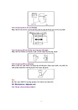
Page 793: ...3 6 Mechanism Adjustment 3 6 1 Name of tape transportation ...

Page 794: ... Driver 1 Turns power off 2 Close the pinch roller to the capstan shaft 3 Press the pinch solenoid by your hand and touch the pinch roller with the capstan shaft 4 Loosen the 2 screw A and adjust B portion so that the Gap T is in the specification by VFK0357 5 Tighten the 2 screw A after adjustment Plate C Plate D Spring Z Gap T Plate C Plate D Gap T ...

Page 795: ... to A direction CW 4 Confirm the reel torque is in the specification when the brake is released and the reel starts rotation 5 Confirm T Reel torque in the same way with S Reel torque 6 Remove the Adaptor VKK1152 and attach the adaptor with the torque meter VFK1191 7 Attach the torque meter with the S Reel table and rotate it to B direction CCW 8 Confirm the reel torque is in the specification whe...

Page 796: ...54 as shown in the figure and adjust the post height 3 Adjust the S1 and T1 post height by VFK1149 and adjust T3 and T4 by VFK1151 Name Limit Post Driver S5 Post Note 1 VFK1149 S4 Post Note 1 VFK1149 T3 Post Lower Limit VFK1151 2 5mm Nut Box T4 Post Lower Limit VFK1151 2 5mm Nut Box Note 1 Rotate CCW one turn from the lower limit VFK1153 VFK1154 VFK1154 VFK1154 VFK1154 VFK1153 Lower Limit Upper Li...

Page 797: ...Arm Adjustment Procedures Start Neutral Position Adjustment Offset Voltage Adjustment Tension Regulator Spring Adjustment Playback Voltage Adjustment OK End REV Voltage Confirmation OK NG NG REV Tension Confirmation ...

Page 798: ...stment VR1 Mech IF Mode EJECT M EQ Digital Volt Meter 1 Set the VTR in EJECT mode and confirm the voltage at TP201 is in the specification 2 If it is not adjust VR1 on the Mech I F Board so that the voltage is in the specification VR2 VR1 S Brake Solenoid Side View Mech I F S Brake Solenoid S Reel Mech chassis ...

Page 799: ...ode 3 Adjust the Tension Regulator Board Base Position so that the voltage at TP201 is in the specification in STOP mode To adjust the Tension Regulator Board Base Position loosen the screw A and move the knob D portion by a screw driver without magnetization and tighten the screw A 4 To set the VTR in no tape loading mode set the DIP SW1 at the rear panel ON to open the service menu Then select T...

Page 800: ...nd Stopper 2 Confirm the voltage at TP201 is in the specification 3 If it is not adjust VR2 Mech I F so that the voltage is in the Specification 4 Then set VFK1155 5 Set the VTR in no tape loading mode and confirm the voltage at TP201 is in the specification in STOP mode If it is not adjust Tension Arm Neutral Position Adjustment again If is out of specification after this adjustment replace the t...

Page 801: ...on Meter 1 Set the VTR in no tape loading 2 Press the tension post by the Dial Tension Meter to R direction in STOP mode 3 Read the Dial Tension Meter when the voltage is 3 8 V PLAY position at TP201 and adjust the Tension Regulator Spring Hook B 4 To adjust the Tension Regulator Spring Hook B position loosen the Tension Regulator Spring position and after adjustment tighten the screw C loose tigh...

Page 802: ...e 1 Place the VTR into no tape loading 2 Press the tension post by the Dial Tension Meter to R direction in STOP mode 3 Read the Dial Tension Meter when the voltage is 1 2 V REV position at TP201 and adjust the Tension Regulator Adjustment again 4 Grew the screw A B and C after Tension Arm adjustment The grew quantity at B is half of A and C B A ...

Page 803: ...l VFK1145 Tension Meter 1 Playback the beginning of 63min M cassette 2 Set a tension meter between S3 and S4 post 3 Confirm the tension is in the specification 4 Set the VTR is in REV mode 5 Set the tension meter between S4 and S5 posts 6 Confirm the tension is in the specification Do not damage a tape during measurement ...

Page 804: ...3 21 Azimuth A C Head Horizontal Adj 3 22 REV Confirm T4 Height Adj 3 23 CTL REC PB Output Level Confirm 3 24 PLAY Limit Confirm 3 25 REV REW FF ENV Confirm 3 26 ENV Rising Confirm 3 27 REV Limit Confirm 3 28 FF REW Limit Confirm 3 29 A C Head T3 T4 Post Screw Grew NG NG NG NG PLAY NG REV T4 Adj Posts A C Head Adj S4 Post Confirm Posts Confirm Posts Confirm END PG LISTA Adj OK OK OK OK OK OK OK OK...

Page 805: ...of the alignment tape 2 Adjust S1 and T1 post height so that the R P envelope output is in the specification 3 When the S1 and T1 posts are adjusted first raise the post height and make small the entrance and exit side of the envelope then down the post until envelope becomes flat 4 Adjust T1 post and makes exit side of the envelope flat then adjust S1 post 5 After the adjustment unload the tape t...

Page 806: ...t is as shown in figure if it is not adjust the post height 2 Confirm that there is no tape problem as D E F in the figure Post Limit Adjustment S5 Free or Lower Limit S5 Post Height S4 Lower Limit S4 Post Height S1 Upper Limit Linearity Coarse T1 Upper Limit Linearity Coarse T3 Lower Limit T3 Post Height T4 Free or Lower Limit T4 Post Height A Upper B Free C Lower D Curl E Bend F Drop ...

Page 807: ...ustment tighten screw H to fix the A C Head Height Screw Tool A VFK1178 0 89 mm Nut Driver B VFK1150 5 5 mm Nut Driver F VFK1148 1 5 mm Nut Driver C D G VFK1209 Torque Driver VFK0912 1 5 mm Hex Driver Bit H VFK1190 1 5 mm L type Hex Wrench P Each Adjustment must be done keeping the screw G tighten Q When tilt is adjusted confirm the screw A is tighten A C Head must be touch with the fix plate R Wh...

Page 808: ... is at lower limit at T3 Post 2 For this Adjustment loosen screw G and make tape curling at T3 lower flange then gradually tighten screw G to make the tape flat The screw G tightening torque is 1 0 Kg cm Reference 1 Screw A CW Tape up Screw A CCW Tape down 2 It is necessary to tighten the each adjustment screw when the adjustment is completed 3 Confirm and adjust alternately this adjustment and A ...

Page 809: ... TP30 on Servo F1 board to observe CTL level 2 Confirm that CTL level is decreased when A C head is up and down at the point shown in the figure If the CTL level is increased adjust nut B so that the CTL level is max 3 Tighten screw H with 2 0 Kg cm torque then confirm the CTL level again Reference 1 Confirm and adjust alternately this adjustment and A C Head each adjustment Azimuth and Height Tap...

Page 810: ...KM No 1 M EQ Oscilloscope Tool VFK1148 Hex Wrench 1 Connect a scope to TP30 on Servo F1 board Then adjust A C Head Azimuth by the screw F so that the CTL level is max 2 For this Adjustment loosen screw G and adjust screw F then tighten screw G Reference Confirm and adjust alternately this adjustment and A C Head each adjustment Azimuth and Height ...

Page 811: ... 2 Confirm that screw G and H are tighten 3 Connect a scope to TP101 and move the tension arm to B direction until T2 post is not moved then confirm the output level variation is in the specification 4 If it is not loosen screw G and adjust screw A then tighten screw G with 1 0 Kg torque 5 It is necessary to complete the adjustment with screw A tighten and confirm that screw A is not loosen 6 If t...

Page 812: ...t a scope to TP101 and raise the A C head or push down it to confirm the CTL level is not increased 3 If it is increased slightly adjust the A C Head Height Adjustment and confirm the CTL level is correct 4 If A C Head Height is changed the azimuth is changed also Therefore A C Head azimuth must be adjusted and confirm alternately 5 When A C Head Height is fixed tilt is changed by tightening screw...

Page 813: ..._SW High or Low is changed at each tape loading 4 Adjust A C Head Horizontal Position so that the memorized H_SW and CTL trigger at the frame start is matched The frame start CTL is located at the falling edge between 6 4 and 5 5 portion To adjust the Horizontal position loosen screw C and D then adjust horizontal position by eccentric driver at hole E 5 After adjustment hit gently at L portion to...

Page 814: ...ation and repeat this adjustment until the specification is satisfied 3 Specification CTL level in REV x 1 speed is more than 75 of Playback CTL level Tape runs in lower limit at T3 Post and tape has no curling and bending at T3 T4 upper and lower limit 4 If the Specification is not satisfied use height adjustment tool T4 Nut Adjustment Direction T4 Nut Adjustment Direction REV CTL Output REV T3 P...

Page 815: ...1 Set the VTR to 25M Mode and record a color bar signal and playback the just recorded portion Then observe the CTL 2 The CTL level is in the specifications in the following table CTL Output Level C1 C2 PLAY REV 1 REV 0 2 C1 C2 1 8V C1 C2 1 4V C1 C2 1 2V 1 If the PLAY Output Level is NG Then confirm the A C Head Height 2 If the REV Output Level is NG Then confirm the T4 Post Height C1 C2 ...

Page 816: ...G NG S4 S5Post Post Height Pre Adj S1 Post OK NG NG NG NG NG S1Post Envelope waveform Adj T1 Post OK NG NG NG NG NG T1Post Envelope waveform Adj T3 Post NG NG OK NG NG NG A C Head Tilt A C Head Tilt Adj T4 Post NG OK OK NG NG NG T4 Post Post Height Pre Adj 1 Playback a Tape and confirm the tape limit at each post is as shown in the above table 2 If it is not adjust each item according with the Adj...

Page 817: ...int TP201 ENV RFEQ H3 Mode REV REW FF Tape VFM3580KM No 1 M EQ Oscilloscope 1 Place the VTR in REV REW FF and confirm that the Waveform is the same diamond style 2 Peak level V is always in the following specification V Vmax 0 9 3 If it is not confirm the S4 Post Height m f n j ...

Page 818: ...assette 123 min pre recorded Tape begin M EQ Oscilloscope This Adjustment must be done after Envelope waveform Adjustment 1 Confirm that the envelope waveform becomes stable immediately in the following transition mode REW to PLAY REV to PLAY FF to PLAY Loading completion to PLAY 2 If it is not confirm S4 Post Height n j m f ...

Page 819: ...mit Refer to Figure A B C D E F S5 Post OK OK OK NG NG NG Tension Post NG OK OK NG NG NG S1 Post OK NG NG NG NG NG T1 Post OK OK OK NG NG NG T3 Post NG NG OK NG NG NG T4 Post NG NG OK NG NG NG 1 Run a tape in Reverse mode and confirm that the tape limit is as shown in the above table 2 This confirmation is done after each adjustment F Drop E Bend D Curl C Lower B Free A Upper ...

Page 820: ... Limit Refer to Figure A B C D E F S5 Post OK OK OK NG NG NG Tension Post NG OK OK NG NG NG S1 Post OK NG NG NG NG NG T1 Post OK OK OK NG NG NG T3 Post OK OK OK NG NG NG T4 Post OK OK OK NG NG NG 1 Run a tape in FF REW mode and confirm that the tape limit is as shown in the above table 2 This confirmation is done after each adjustment F Drop E Bend D Curl C Lower B Free A Upper ...

Page 821: ...3 mm About 5 mm 1 Grew after A C Head Adjustment 2 Remove the screw grew before Adjustment T3 Post T4 Post Grew T3 Post T4 Post Grew amount About 3 mm About 5 mm 1 After A C Head Adjustment grew the Plastic Nut part of T3 and T4 posts 2 Remove the screw grew before Adjustment Plastic Nut Grew T4 Post ...

Page 822: ... Linearity 25M Mode Linearity Adj Waving Measure PB Sensitivity 25M Mode Sensitivity Sensitivity Detection Sensitivity Adj Sensitivity Detection Linearity Adj 50M Mode Linearity Adj Waving Measure PB Sensitivity Adj 25M Mode Sensitivity Sensitivity Detection END RFEQ ENV Level Adj Lch Rch R P Sensitivity 50M Mode ...

Page 823: ...he LISTA clips to the following Test Points 1 ATF TP732 2 HSW TP722 RP HSW or TP723 PB HSW 3 GND TG510 3 Run the LISTA software Installation and Operation Make a directory like C LISTA and copy the all files in the floppy disk of VFK1420 Type Lista50 exe in the DOS mode to run the LISTA software 4 Select the model of AJ D950 in the menu 5 Select a alignment tape to use LISTA Adjustment If it is no...

Page 824: ...ntry is displayed input the tape serial number according with the menu instruction The serial number is stumped on the alignment tape Then select the PAL or NTSC Type 0 or ENTER to choose DVCPRO 4 Then input the all data 37 items for NTSC and check sum IF the data is incorrect registration is not completed so check and input again After data registration select 1 SELECT ...

Page 825: ... in 25M Mode Select AJ D950 in the PC menu and displays the main menu 25M and 50m mode can be changed by 0 key 1 Set the VTR in Service Mode to open the service menu and select the item of A09 RP GAIN DP in the SERVO ADJUST menu 2 Playback a LISTA alignment tape VFM3581KM 3 Select the LISTA 6 ATF Error Signal Monitor and 1 2 Speed and type Enter to start the software 4 When the picture is appeared...

Page 826: ...KL Before this adjustment RP Head Sensitivity Adjustment 25M Mode must be completed 1 Select A09 RP GAIN DP in the Service Menu 2 Playback a LISTA Alignment Tape VFM3581KM 3 Select LISTA Main Menu 1 Sensitivity Measurement Press enter when 1 2 Speed is appeared to start the Sensitivity measurement 4 Confirm that the specification is satisfied when Sensitivity Measurement Finish and Sensitivity sen...

Page 827: ...he following waveform is appeared press BS Back Space key to centering the waveform Adjust S1 and T1 Post Height so that the Linearity waveform is flat Confirm the ENV waveform is flat Red dot lines shows the specification so linearity waveform should be in the lines Points 1 The left of linearity Entrance is changed by S1 Post Height and right of linearity Exit is changed by T1 Post Height 2 Lowe...

Page 828: ...ys together and Waving value is displayed at left bottom of the monitor Then confirm the waving is 1 5 um or less and the waving is constant from the entrance to exit If the waving is out of specification adjust S1 Entrance and T1 Exit Post Height 3 After measurement press ESC key to return the main menu Adjustment Value Adjustment Value ...

Page 829: ... VFM3581KM or VFM3581KL 1 Open the Service Menu and select A11 PB GAIN DP in the SERVO ADJUST menu 2 Playback a LISTA alignment Tape VFM3581KM 3 Select LISTA Main Menu 6 ATF Error Signal Monitor Press enter when 1 2 Speed is appeared to start the Sensitivity measurement 4 When the picture is appeared as shown in figure adjust ATF Gain so that the Sens Value his in the Specification 5 After Adjustm...

Page 830: ...Before this adjustment PB Head Sensitivity Adjustment 25M Mode must be completed 1 Open the Service Menu and select A11 PB GAIN DP 2 Playback a LISTA alignment tape VFM3581KM 3 Select LISTA Main Menu 1 Sensitivity Measurement Press enter when 1 2 Speed is appeared to start the Sensitivity measurement 4 Confirm that the specification is satisfied when Sensitivity Measurement Finish and Sensitivity ...

Page 831: ...e PC menu and displays the main menu 25M and 50m mode can be changed by 0 key 2 Set the VTR in Service Mode to open the service menu and select the item of A05 RP GAIN ED in the SERVO ADJUST menu 3 Playback a LISTA alignment tape VFM3581KM 4 Select the LISTA 6 ATF Error Signal Monitor and 1 2 Speed and type Enter to start the software 5 When the picture is appeared as shown in figure adjust ATF Ga...

Page 832: ...KL Before this adjustment RP Head Sensitivity Adjustment 25M Mode must be completed 1 Select A05 RP GAIN ED in the Service Menu 2 Playback a LISTA Alignment Tape VFM3581KM 3 Select LISTA Main Menu 1 Sensitivity Measurement Press enter when 1 2 Speed is appeared to start the Sensitivity measurement 4 Confirm that the specification is satisfied when Sensitivity Measurement Finish and Sensitivity sen...

Page 833: ...the Service Menu and select A06 RP LINEAR ED in the SERVO ADJUST 2 Playback a LISTA alignment Tape VFM3581KM 3 Select 2 Linearity Measurement then Linearity waveform is appeared 4 When the following waveform is appeared press BS Back Space key to centering the waveform Adjust S1 and T1 Post Height so that the Linearity waveform is flat Confirm the ENV waveform is flat Red dot lines shows the speci...

Page 834: ...and keys together and Waving value is displayed at left bottom of the monitor Then confirm the waving is 1 5 um or less and the waving is constant from the entrance to exit If the waving is out of specification adjust S1 Entrance and T1 Exit Post Height 3 After measurement press ESC key to return the main menu Adjustment Value ...

Page 835: ...pe VFM3581KM or VFM3581KL 1 Open the Service Menu and select A07 PB GAIN ED in the SERVO ADJUST menu 2 Playback a LISTA alignment Tape VFM3581KM 3 Select LISTA Main Menu 6 ATF Error Signal Monitor Press enter when 1 2 Speed is appeared to start the Sensitivity measurement 4 When the picture is appeared as shown in figure adjust ATF Gain so that the Sens Value is in the Specification After Adjustme...

Page 836: ...M3581KL Before this adjustment PB Head Sensitivity Adjustment 50M Mode must be completed 1 Open the Service Menu and select A07 PB GAIN ED 2 Playback a LISTA alignment tape VFM3581KM 3 Select LISTA Main Menu 1 Sensitivity Measurement Press enter when 1 2 Speed is appeared to start the Sensitivity measurement 4 Confirm that the specification is satisfied when Sensitivity Measurement Finish and Sens...

Page 837: ... Point TP201 R P ENV L H3 R H4 Adjustment S1 T1PostHeight Mode PLAY Tape VFM3580KM No 1 M EQ Oscilloscope Tool VFK1149 Post Driver 1 Playback an alignment Tape 2 Confirm the R P Envelope Level is in the specification 3 If it is not adjust ENV waveform Adjustment and LISTA Adjustment ...

Page 838: ...xible cable Note Be careful to remove the flexible cable from the connector Do not touch on the cylinder surface by finger directly 3 Remove the connector P33 on the Mech Interconnection board at bottom of VTR Then remove 3 screws with spring and draw out the cylinder unit without touching any parts Note Do not touch the cylinder surface by finger directly Installation of cylinder 1 Install a Cyli...

Page 839: ...2 Push the Cleaner Solenoid Rotate the cylinder and confirm that the cleaner roller is rotated by the cylinder movement 3 Install a T1 Guide 4 After T1 Guide installation T1 Guide position adjustment is necessary 3 7 3 T1 Guide Position Adjustment 1 Set the VTR in no tape loading mode No tape loading procedures Open the Servo Adjust menu in the Service Menu Select the item T TORQUE and press the s...

Page 840: ...ment Tension Confirmation A C Head Azimuth H Position Confirmation A C Head Height Confirmation A C Head Tilt Confirmation A C Head Confirmation Post Limit Confirmation Envelope Waveform Adjustment REV Tape Run Confirmation LISTA Servo Menu Setting LISTA Connection LISTA A C Head T3 T4 Post Grew REV REW FF ENV Limit Confirmation PLAY Limit Confirmation CTL REC PB Output Level Confirmation 25M Mode...

Page 841: ...n remove A C Head 4 Remove 2 screws D and remove the shield case 5 Unsolder the Lead wire from the A C Head When unsolder the lead wires do not unsolder all at the same time Installation of A C Head 1 Remove the shield case from a new A C Head and solder the each lead wires 2 Install the shield case 3 Install the A C head to the A C head plate by 2 screws A Then set to parallel the gap between A C...

Page 842: ... adjustment completion 2 A C Head Adjustment and Confirmation are shown in the following flow chart A C Head Side Cable Color Connector No 1 PINK YELLOW 2 WHITE 3 PINK RED P1 4 WHITE 5 PINK GREEN 6 WHITE 7 WHITE YELLOW P30 8 BLACK Start A C Head Tilt Adjustment REC PB Envelope Adjustment LISTA PG Shifter Adjustment A C Head Azimuth H Position Adjustment A C Height Adjustment End A C Head Tape Path...

Page 843: ... position of Reel Base which is inserted the pin of Drive Arm Unit The position can remember by the attached grease Installation of Supply and Take up Reel Unit 1 Insert the outer rail at the new Reel Table 2 Hook the Reel Table Unit at the inner rail Then install a Reel Table so that its groove is matched with the pin of Drive Arm Unit 3 Tighten 4 screws C D and E then confirm the Reel Table move...

Page 844: ...Mech IF Board Removal Reel Rotor Unit Installation of Reel Rotor Unit ...

Page 845: ...rake Torque Refer to the Main Brake Torque Confirmation Reel Brake Arm Unit Replacement 3 7 9 Supply Brake Solenoid Replacement and Adjustment Removal of Supply Brake Solenoid 1 Remove the top panel 2 Remove the front loading unit 3 Remove the bottom panel 4 Remove the connector P15 on Mech Interconnection board 5 Remove 2 screws A and remove the Supply Brake Solenoid Base Unit 6 Remove 2 screws B...

Page 846: ...Solenoid Replacement and Adjustment Removal of Take up Brake Solenoid 1 Remove the top panel 2 Remove the front loading unit 3 Remove the bottom panel 4 Remove the connector P18 on the Mech Interconnection board 5 Remove 2 screws A and remove the take up brake solenoid base unit 6 Remove 2 screws B and remove the Brake Solenoid from the Take up Brake Solenoid Base Unit Take up Brake Solenoid Remov...

Page 847: ...to Pinch Solenoid Position Adjustment Pinch Solenoid Removal 3 7 12 Pinch Arm Unit Replacement Removal of Pinch Arm Unit 1 Remove the top panel 2 Remove the front loading unit 3 Remove the bottom panel 4 Disconnect the connector P20 on the Mech Interconnection board 5 Remove the Pinch Solenoid Unit 6 Remove 2 Screws A and remove the Pinch Solenoid Unit 7 Remove the cut washer B and remove the Pinc...

Page 848: ...oove position of main Cam Gear 3 Install the emergency shaft with screw B 4 Install the Pinch Solenoid Unit After installation adjust Pinch Solenoid Position Adjustment Refer to Pinch Solenoid Position Adjustment 5 Connect the connector P21 Removal of Loading Motor 3 7 14 Mode Switch Unit Replacement Removal of Mode Switch Unit 1 Remove the top panel 2 Remove the front loading unit 3 Remove the bo...

Page 849: ...e Pinch Solenoid Unit and Loading Motor Neutral Unit Refer to Loading Motor Replacement and Pinch Arm Unit Replacement 4 Remove the Main Cam Gear Installation of Main Cam Gear 1 Install a new Main Cam Gear in reverse order of its removal For this installation set the pin of the Income Arm Unit to the groove of the Main Cam Gear Removal of Main Cam Gear ...

Page 850: ...p panel 2 Remove the front loading unit 3 Remove the cut washer A and remove the tension regulator spring from its hook then remove the tension arm unit Installation of Tension Arm Unit 1 Install the new Tension Arm Unit as reverse order of its removal 2 After installation adjust tension arm adjustment following the tension arm adjustment flow chart Removal of Tension Arm Unit Tension Arm Adjustme...

Page 851: ...ng Arm Unit Installation of S1 Post Loading Arm Unit 1 Install a new S1 Post Loading Arm Unit as reverse order of removal After its installation S1 Post Loading Arm Unit Phase Adjustment is necessary 2 After its installation confirm the S1 Post moves smoothly on the loading rail Then Adjust the Tension Arm and Linearity Adjustment Procedure 1 When S1 Post Loading Arm is installed the hole A and B ...

Page 852: ...m the Loading Rail 6 Remove the screw D and E and remove the Loading Rail 7 Remove the T1 Boat Unit from the T1 Loading Unit Installation of T1 Loading Arm Unit 1 Install a new T1 Loading Arm Unit as reverse order of its removal For this installation the following adjustment is necessary Adjustment Procedures 1 Install T1 Loading Arm Unit so that the Hole A and Hole B are in parallel 2 After insta...

Page 853: ... C direction and adjust the clearance D is in the specification 3 Pushthecleanersolenoidshaftandconfirmthatthe cleaner roller touches the cylinder Then confirm that the cleaner roller returns original position when the shaft is released 4 Push the Solenoid shaft and rotate the cylinder and confirm that the cleaner roller is rotated by the cylinder movement Cleaner Solenoid Position Adjustment Clea...

Page 854: ...nt loading unit 3 Remove the connector P24 on the Mech Interconnection board 4 Remove 4 screws A and B and remove the M Stopper Solenoid Installation of M Stopper Solenoid 1 Install a new M Stopper Solenoid as reverse order of its removal 2 After its installation following adjustment is necessary M Stopper Solenoid Removal Adjustment Procedures 1 Set the Reel Table at L cassette position 2 Release...

Page 855: ...Rail Unit as reverse order of its installation 2 Confirm that M and L cassette touches MIC Rail Unit MIC Rail Unit Removal 3 7 26 Reel Drive Motor Unit Replacement Removal of Reel Drive Motor Unit 1 Remove the top panel 2 Remove the front loading unit 3 Remove the connector P16 on the Mech Interconnection board 4 Remove 2 screws A and remove the Reel drive sensor board 5 Remove 2 screws B and remo...

Page 856: ...r Unit Replacement 5 Remove the cut washer A and remove the Reel Drive Cam Gear 6 Remove the cut washer B and remove the MIC Drive Arm Unit 7 Remove the cut washer and remove the MIC intermittent gear 8 Remove the cut washer D and remove the Reel Drive Arm Unit 9 Remove the supply and take up reel rotor unit Refer to Supply and Take up Reel Table Unit Replacement 10 Remove the cut washer E and rem...

Page 857: ... 1 Close the Reel Table to M Cassette position 2 Set the MIC SW Distinction SW to the nearest position from the Reel 3 MIC Drive Arm Unit Pin position is as shown in the above figure 4 Reel Drive Came Gear Hole and MIC Intermittent Gear phase are matched 3 7 29 T4 Post Position Adjustment 1 Set the VTR unloading condition 2 Confirm the T4 post hole is at the T4 connection gear B 3 Confirm that and...

Page 858: ...tan housing 3 While rotating the capstan shaft CCW tighten the thrustscrewCWslowlyandstopitwhentherotation becomes smoothly 4 Rotate another 180 degrees or 270 degrees from the stop position of item 3 5 Grew the thrust screw 6 Confirm the oil seal as shown in figure Thrust Screw Capstan Housing Oil Seal Thrust Screw Oil 0 270 225 180 ...

Page 859: ...RIMMER ADJUSTMENT DRIVER 1 VFK1156 NEUTRAL POSITION TOOL BLACK 1 VFK0337 PHILIPS DRIVER 1 VFK1208 NEUTRAL POSITION TOOL 1 VFK1369 TAPE SENSOR CASSETTE 1 VFK1150 NUT DRIVER 5 5mm 1 VFK0908 HYDRAULIC FLUID 1 VFK1151 NUT DRIVER 2 5mm 1 VFM3000EDS ALIGNMENT TAPE DV LISTA 1 VFK1188 DIAL TENSION GAUGE 30g 1 VFM3580KM ALIGNMENT TAPE No 1 1 FOR NTSC VFK0948 CHECK LIGHT 1 VFM3581KM ALIGNMENT TAPE No 2 1 FO...

Page 860: ... Y 7 VEM0645 LOADING MOTOR 1 AU 1 MECHANICAL CHASSIS ASS Y 55 VXQ0556 THRUST SCREW U 1 MECHANICAL CHASSIS ASS Y 8 VSJ0227 PINCH SOLENOID 1 MECHANICAL CHASSIS ASS Y VXY1318Z1 MECHANISM 1 MECHANICAL CHASSIS ASS Y 10 VES0714 MODE SW U 1 MECHANICAL CHASSIS ASS Y 8 VEM0585 REEL DRIVE MOTOR U 1 SUB CHASSIS ASS Y 12 VXL2748 CLEANING ARM AU 1 MECHANICAL CHASSIS ASS Y 14 VSJ0216 BRAKE SOLENOID 3 SUB CHASSI...

Page 861: ...PRT 3 MECHANICAL CHASSIS ASSEMBLY 1 ...

Page 862: ...NER RAIL 2 5 VXL2589 S BASE DRIVE ARM U 1 6 VMB2944 CHARGE SPRING 2 7 VXL2590 T BASE DRIVE ARM U 1 8 VXA5625 SLIDE ROD U 1 9 VXL2597 M STOPPER DRIVE ARM U 1 9 1 VMB2955 M STOPPER SPRING 1 1 9 2 VMB3017 M STOPPER SPRING 2 1 10 VXA6174 L M RELEASE ANGLE ASS Y 1 11 VXZ0424 S BRAKE ARM UNIT 1 12 VXZ0425 T BRAKE ARM UNIT 1 31 VMX1061 WASHER 7 32 VMX1079 CUT WASHER 2 33 VMX1394 CUT WASHER 2 34 XQN2 CF3 ...

Page 863: ...PRT 5 MECHANICAL CHASSIS ASSEMBLY 2 Components identified with the mark have the special characteristics for safety When replacing any of these components use only the same type ...

Page 864: ... WASHER 1 16 VXL2812 S1 LOADING ARM N ASS Y 1 M VXY1318Z1 MECHANISM 1 M 17 VMD2533 LOADING RAIL 1 18 VXA6108 T1 BOAT U ASS Y 1 M 19 VHD0561 HEX SCREW 1 20 VXA6052 S POST BASE AU 1 M 21 VXP1683 T4 CONNECTION GEAR U 1 22 VXL2772 T4 ARM U 1 23 VMB2950 T4 THRUST SPRING 1 24 VXL2842 T LOADING ARM N ASS Y 1 25 VMS5906 T3 UPPER FRANGE 1 26 VMS5905 T3 SLEEVE 1 27 VMS5904 T3 LOWER FRANGE 1 28 VMB2929 T3 SP...

Page 865: ...PRT 7 SUB CHASSIS ASSEMBLY ...

Page 866: ...MOTOR BASE U 1 12 VMB3019 MIC DRIVE RETURN SPRING 1 13 VEK7726 REEL SENSOR P C BOARD 1 14 VSJ0216 BRAKE SOLENOID 3 M 15 VXA5575 S BRAKE SOLENOID BASE U 1 17 VXA6199 DISTINCTION SW ASS Y 1 M 18 VXA5579 M STOPPER SOLENOID U 1 19 VXA5887 T BRAKE SOLENOID BASE U 1 20 VXK1336 SUB CHASSIS 1 21 VEK7692 SENSOR HOLDER U 1 22 VMS6193 T BRAKE RELEASE ARM SHAFT 1 23 VMB2957 S BRAKE SPRING 1 24 VMB2987 T BRAKE...

Page 867: ...CASSETE COMPARTMENT ASSEMBLY PRT 9 ...

Page 868: ...6 WORM WHEEL 1 32 VXA5848 MOTOR ANGLE A ASS Y 1 33 VXP1797 E E SLOT IN WORM ASS Y 1 34 VXA5597 MOTOR ASS Y 1 M 35 VMA9673 EMARGENCY ANGLE 1 36 BRK7793 MOTOR P C BOARD 1 37 VMA9668 HOLDER PLATE 1 38 VEK7715 HOLDER FLEXIBLE ASS Y 1 39 VXA6075 MAIN RACK L ASS Y 1 40 VML2A49 WIPER ARM L 1 41 VMB2925 WIPER SPRING L 1 42 VDG1163 WIPER GEAR 2 43 VMB3013 WIPER SPRING R 1 44 VML2A52 WIPER ARM R 1 45 VDP164...

Page 869: ...FRONT PANEL ASSEMBLY PRT 11 ...

Page 870: ...IAL 1 24 VMP4860 VR ANGLE 1 25 VKU0513 BACK COVER 1 25 VKU0524 BACK COVER 1 AJ D950E 26 VMB2978 LEAF SPRING 2 27 VGM1288 SUB CONTROL SUPPORT ANGLE 1 28 VGM1287 SUB CONTROL ANGLE 1 29 VGM1440 SUB SW ANGLE 1 30 VGU7179 SLIDE SW KNOB 10 31 VGU7178 VR KNOB 5 32 VWJ28C2120LFR CPU SUB FFC 1 33 VMS6012 SHAFT 1 34 VKF2497 SUB SW DOOR 1 35 VMC1241 EARTH PLATE 1 36 VMP5091 EARTH PLATE SUB 1 37 VMP4863 CASSE...

Page 871: ...Components identified with the mark have the special characteristics for safety When replacing any of these components use only the same type PRT 13 REAR PANEL ASSEMBLY ...

Page 872: ...NLET BRACKET 1 15 XBA1C50NB5 FUSE 1 AJ D950P PD950P 15 XBA2C40TH15FUSE 1 AJ D950E 16 VJF1005 FUSE HOLDER 1 17 VJF0285 WIRE LOCKING SADDLE 1 18 VMP5613 BLANK PANEL 1 19 VJS4132 BNC 1 20 VMP5743 SR HOLD BASE 1 21 VMP5744 SR HOLD ANGLE 1 22 VMT0917 SH HOLD CUSHION 1 71 VHD0426 SCREW 1 72 XSN26 6FZ SCREW 22 73 XSN4 35FC SCREW 2 74 XTN26 6FFZ SCREW 1 75 XTV3 6F SCREW 5 76 XTV3 6FFZ SCREW 2 77 XTV3 6FFR...

Page 873: ...PRT 15 CASING PARTS ASSEMBLY ...

Page 874: ...KU0514 BOTTOM PLATE 1 10 VMX1558 NYLON WASHER 2 11 VEE9641 FRONT CABLE 1 12 VMX2582 WASHER 2 13 VMP5265 CARRIAGE SUPPORT METAL 1 14 VMT0797 DUST PROOF CUSHION A 1 AJ D950P PD950P 14 VMT0493 GASKET A 1 AJ D950E 15 VMT0509 GASKET B 1 AJ D950E 16 VMT0800 GASKET C 7 AJ D950E 17 VMT0776 GASKET D 2 AJ D950E 18 VMT0797 DUST PROOF CUSHION A 3 19 VMT0785 DUST PROOF CUSHION B 1 20 VMT0786 DUST PROOF CUSHION...

Page 875: ...CHASSIS FRAME ASSEMBLY PRT 17 Components identified with the mark have the special characteristics for safety When replacing any of these components use only the same type ...

Page 876: ...P4872 SIDE FRAME R 1 23 VJF0384 CLAMPER 2 24 VSC4528 PROTECT SHEET 1 AJ D950P PD950P 25 VMP5264 FPC SHIELD COVER 1 26 VSC4384 POWER WIRE COVER 1 AJ D950E 27 VMC1318 FRAME EARTH METAL 1 AJ D950E 28 VMP5263 WIRING SHIELD COVER 1 AJ D950E 29 VMT0496 GASKET 1 30 VMP5285 BOTTOM FRAME ANGLE 4 31 VGF0714 BARRIER A 1 71 VHD5013 SCREW 2 72 XTN3 6F SCREW 2 73 XTV3 6F SCREW 43 74 XTV3 6FFR SCREW 9 75 XYN3 C6...

Page 877: ...PACKING PARTS ASSEMBLY PACKING PARTS ASSEMBLY PRT 18 Components identified with the mark have the special characteristics for safety When replacing any of these components use only the same type ...

Page 878: ...3 VQT7275 OPERATING INSTRUCTIONS 1 AJ D950P PD950P 3 VQT7276 OPERATING INSTRUCTIONS 1 AJ D950E 4 VPN4302 CUSHION UL 1 5 VPN4304 CUSHION LL 1 6 VPN4606 CUSHION UR 1 7 VPN4607 CUSHION LR 1 8 VPF0277 POLYETHYLENE BAG 1 AJ D950P PD950P 8 VPF0673 POLYETHYLENE BAG 1 AJ D950E 9 VPG9197 PACKING CASE 1 AJ D950E 9 VPG9278 PACKING CASE AJ PD950P 9 VPG9196 PACKING CASE 1 AJ D950P 10 VPF0149 HANDLE 2 11 VXF015...

Page 879: ...PACKING PARTS ASSEMBLY Components identified with the mark have the special characteristics for safety When replacing any of these components use only the same type ...

Page 880: ...f No Part No Part Name Description Pcs Remarks Ref No Part No Part Name Description Pcs Remarks 1 VPG8524 PACKING CASE 1 2 VQT7283 OPERATING INSTRUCTION 1 3 VPF0680 AIR CAP 2 4 VPF0506 EARTH BAG 2 5 VQL8468 PACKING LABEL S 1 ...

Page 881: ...AUDIO JACK P C BOARD VEP84303B FOIL SIDE COMPONENT SIDE ...

Page 882: ...C225 B3 IC240 D4 REF LOC IC241 C4 IC260 E4 IC262 E4 IC270 G4 IC272 E3 IC273 F4 IC274 F4 IC275 G3 IC276 E3 IC277 G3 IC279 F3 IC280 E3 IC330 G2 IC331 F2 REF LOC IC332 F2 IC333 D3 IC334 F3 IC350 J2 IC352 J3 IC353 I2 IC354 I1 IC355 I1 IC357 H1 IC359 J1 IC390 G2 IC392 I3 IC393 H2 IC394 H1 REF LOC REF LOC IC395 H1 IC397 G1 IC450 H2 IC451 I2 IC452 I3 IC490 H2 IC491 G2 IC492 I2 IC590 F2 IC591 F3 IC622 F2 ...

Page 883: ...IC531 G3 IC600 C4 REF LOC IC620 E1 IC621 E2 IC700 A4 IC701 A1 IC701 A1 P1 G5 P1 G5 P2 D5 P2 D5 P650 D1 P650 D1 P670 G1 P670 G1 P700 B1 REF LOC P700 B1 SW600 C4 SW601 C4 TG1 A1 TG2 A4 TG3 D1 TG4 F5 TG5 I3 TG6 I4 TP20 C4 TP21 E4 TP22 C4 TP130 C1 TP131 C1 REF LOC REF LOC TP132 B1 TP161 C2 TP162 C2 TP163 C2 TP240 C4 TP241 C4 TP242 C4 TP243 C4 TP330 E1 TP331 E1 TP332 E1 TP333 F1 TP334 E1 TP350 J3 TP351...

Page 884: ...03 H2 IC4304 G2 IC4306 H1 IC4351 B1 IC4353 B2 IC4354 A2 IC4356 A1 IC4402 I5 IC4403 I5 IC4404 H2 IC4405 H3 IC4406 H2 IC4477 G2 IC4478 G3 IC4479 G2 IC4552 B5 IC4553 A5 IC4554 B2 IC4555 B3 IC4556 B2 IC4627 A2 IC4628 A3 IC4629 A2 IC4701 E1 IC4703 F1 IC4704 D1 IC4707 G1 IC4708 G1 IC4709 G2 IC4710 G2 IC4711 E1 IC4712 F2 IC4713 D1 IC4751 F1 IC4752 G1 IC4831 E2 IC4832 E2 IC4901 D4 IC4933 E4 IC4934 F4 IC49...

Page 885: ...1 IC4307 H2 IC4308 G1 IC4352 B1 IC4355 B1 IC4357 B2 IC4358 A1 IC4401 H2 IC4407 G4 IC4408 H4 IC4476 G2 IC4480 G4 IC4481 G4 IC4551 B2 IC4557 B4 IC4558 B4 IC4626 A2 IC4630 A4 IC4631 A4 IC4702 F1 IC4753 F2 IC4754 F2 IC4755 G1 IC4756 G1 IC4757 F2 IC4758 G2 IC4833 D2 IC4834 E2 IC4835 E1 IC4836 D1 IC4837 E2 IC4838 D2 IC4931 E4 IC4932 F4 IC4935 F4 IC4938 F3 IC4939 E3 IC4940 E3 Q350 B2 Q351 B2 Q352 B2 Q353...

Page 886: ...AES EBU P C BOARD VEP84304A FOIL SIDE COMPONENT SIDE ...

Page 887: ...AJOG SUB P C BOARD VEP84313A FOIL SIDE COMPONENT SIDE ...

Page 888: ...AMEM SUB P C BOARD VEP84314A FOIL SIDE COMPONENT SIDE ...

Page 889: ...BLK SUB P C BOARD VEP83431A ...

Page 890: ...C4009 D4 IC4010 D4 IC4011 C2 IC4012 B1 IC4014 D1 IC4015 C2 IC4016 C2 IC4101 D3 REF LOC IC4102 D3 IC4107 D2 IC4108 E2 IC4109 E2 IC4110 C4 IC4111 E3 IC4112 D4 IC4113 D4 IC4114 E4 IC4201 C3 IC4204 D4 IC4205 C4 REF LOC IC4206 A2 IC4301 A4 IC4302 B4 IC4305 B4 IC4307 B3 IC4308 B3 IC4404 A3 IC4405 A3 IC4407 C3 IC4501 A3 IC4502 A4 IC4504 B4 REF LOC IC4506 B4 IC4507 A3 P4001 C5 P4002 B1 P4003 A1 Q4001 B1 Q...

Page 891: ... IC3030 G4 IC3031 H4 IC3033 B1 IC3034 D1 IC3035 C1 IC3036 D1 IC3037 C1 REF LOC IC3038 G1 IC3039 H3 IC3040 D1 IC3041 C1 IC3042 B1 P3001 C2 P3002 H2 P3003 E1 Q3002 E3 Q3004 F3 Q3005 E3 Q3006 F2 REF LOC Q3007 F2 Q3008 F3 Q3009 F3 Q3010 F2 Q3011 F2 Q3012 F3 Q3013 H2 Q3015 H3 Q3018 H4 Q3021 H2 Q3022 G4 Q3023 G4 REF LOC Q3024 H3 Q3027 H4 Q3028 H4 Q3029 H4 Q3030 H2 Q3031 H2 Q3032 H3 Q3033 H3 ...

Page 892: ...2 IC3021 G3 IC3022 G2 IC3024 G2 IC3025 G2 IC3026 G3 IC3028 H2 IC3029 H3 IC3032 H4 IC3043 C2 IC3044 B2 IC3045 C2 REF LOC IC3046 B2 IC3047 B2 IC3048 A2 IC3049 A3 IC3050 B3 IC3051 A3 IC3052 B3 IC3053 A4 IC3054 B4 Q3001 F2 Q3003 F2 Q3014 H2 Q3016 G4 Q3017 G4 REF LOC Q3019 G4 Q3020 G4 Q3025 H2 Q3026 H2 Q3034 H3 Q3035 H2 TG3001 H1 TG3002 G4 TP3001 G3 TP3002 G1 TP3003 G2 VR3001 F3 VR3002 F3 VR3003 F2 REF...

Page 893: ...DV UCOM P C BOARD VEP88234A FOIL SIDE COMPONENT SIDE ...

Page 894: ...EDA CSP SUB P C BOARD VEP83411A FOIL SIDE COMPONENT SIDE ...

Page 895: ...FRONT CPU SUB P C BOARD VEP86148A ...

Page 896: ...52 D1 Q53 D1 QR1 J3 QR2 J3 QR3 I3 QR4 J2 QR5 J3 QR6 I2 QR7 K1 QR8 I2 QR9 M1 QR10 M1 QR11 L1 QR12 K2 QR13 J2 QR14 F3 QR15 E3 QR16 E3 QR17 M1 QR18 M1 QR19 L1 QR20 J2 QR21 I2 QR22 J1 QR23 I1 QR24 H3 QR25 H3 QR26 G3 QR27 E2 QR28 E2 QR29 E2 QR30 F2 QR31 F2 QR32 E3 QR33 E3 QR34 F2 QR35 F2 QR36 G2 QR37 G2 QR38 G2 QR39 H2 QR40 G3 REF LOC REF LOC REF LOC REF LOC REF LOC REF LOC ...

Page 897: ... SW12 E3 SW13 E3 SW14 H3 SW15 G3 SW16 G3 SW17 E2 SW18 E2 SW19 F2 SW20 F2 SW21 G2 SW22 G2 SW23 H2 SW24 H2 SW25 G3 SW26 H3 SW27 M1 SW28 J1 SW29 J1 SW30 I1 SW31 I1 SW32 H1 SW33 H2 SW34 H2 SW35 H2 SW36 G2 SW37 G2 SW38 G2 SW39 A1 SW40 A2 SW41 A2 SW42 G3 SW43 H3 REF LOC REF LOC REF LOC REF LOC REF LOC REF LOC COMPONENT SIDE FRONT CPU P C BOARD VEP86263A COMPONENT SIDE ...

Page 898: ...52 D1 Q53 D1 QR1 J3 QR2 J3 QR3 I3 QR4 J2 QR5 J3 QR6 I2 QR7 K1 QR8 I2 QR9 M1 QR10 M1 QR11 L1 QR12 K2 QR13 J2 QR14 F3 QR15 E3 QR16 E3 QR17 M1 QR18 M1 QR19 L1 QR20 J2 QR21 I2 QR22 J1 QR23 I1 QR24 H3 QR25 H3 QR26 G3 QR27 E2 QR28 E2 QR29 E2 QR30 F2 QR31 F2 QR32 E3 QR33 E3 QR34 F2 QR35 F2 QR36 G2 QR37 G2 QR38 G2 QR39 H2 QR40 G3 REF LOC REF LOC REF LOC REF LOC REF LOC REF LOC ...

Page 899: ... SW12 E3 SW13 E3 SW14 H3 SW15 G3 SW16 G3 SW17 E2 SW18 E2 SW19 F2 SW20 F2 SW21 G2 SW22 G2 SW23 H2 SW24 H2 SW25 G3 SW26 H3 SW27 M1 SW28 J1 SW29 J1 SW30 I1 SW31 I1 SW32 H1 SW33 H2 SW34 H2 SW35 H2 SW36 G2 SW37 G2 SW38 G2 SW39 A1 SW40 A2 SW41 A2 SW42 G3 SW43 H3 REF LOC REF LOC REF LOC REF LOC REF LOC REF LOC COMPONENT SIDE FRONT CPU P C BOARD VEP86263A COMPONENT SIDE ...

Page 900: ...IC203 E3 IC302 C1 IC303 C1 IC304 C1 IC305 D3 IC306 B2 IC307 B2 IC308 D2 IC309 C2 IC311 C1 IC312 C1 REF LOC REF LOC REF LOC REF LOC REF LOC IC313 B2 IC314 B2 IC315 D2 IC502 C1 IC503 C1 IC506 B3 IC507 B3 IC508 D3 IC509 C3 IC511 C1 IC512 C1 IC513 B3 IC514 B3 IC515 D3 P701 E2 P702 A2 P703 A3 Q301 C2 Q302 B1 Q305 B1 Q306 C2 Q309 C2 Q310 C2 Q311 C2 Q312 C2 Q316 C2 Q319 B2 Q321 C2 Q322 B1 Q325 B1 Q326 C2...

Page 901: ...7 29 MECHANISM I F P C BOARD VEP82216A FOIL SIDE COMPONENT SIDE ...

Page 902: ...7 30 P MOTHER P C BOARD VEP89129A FOIL SIDE ...

Page 903: ...7 31 P MOTHER P C BOARD VEP89129A COMPONENT SIDE ...

Page 904: ...POWER CONNECTION P C BOARD VEP80A58A COMPONENT SIDE FOIL SIDE ...

Page 905: ...POWER 1 P C BOARD VEP81183A COMPONENT SIDE FOIL SIDE ...

Page 906: ...POWER 2 P C BOARD VEP81184A COMPONENT SIDE FOIL SIDE ...

Page 907: ...2 IC29 A3 IC30 C2 IC41 A1 IC43 B3 IC44 B3 IC45 H2 IC46 G3 IC49 I4 IC53 I2 IC54 I3 IC55 H3 IC56 I4 IC58 I1 IC59 I4 IC63 H4 IC68 H2 IC69 I1 IC70 C4 IC71 C4 IC75 C4 IC84 A5 IC85 A5 IC86 B4 IC87 A4 IC88 A4 IC89 E1 IC90 D3 IC91 D3 IC94 B3 IC95 G1 IC103 F1 IC106 G4 IC107 F3 IC108 G4 IC110 G3 IC112 G4 IC113 H4 IC114 F4 IC115 H4 IC116 H3 IC119 H3 IC125 C1 IC126 C2 IC127 D2 IC128 C1 IC129 D1 IC130 D1 IC131...

Page 908: ...C97 E2 IC98 H1 IC99 F2 IC100 F2 IC101 G2 IC102 G2 IC109 G3 IC111 G4 IC117 H4 IC118 H4 IC120 H3 IC121 B1 IC122 D1 IC123 C1 IC124 C2 IC200 C2 IC201 B2 IC800 H4 IC801 F4 IC802 A4 IC803 C4 IC904 E4 P1 G5 P2 C5 P3 E1 P5 H1 P6 H3 P10 F1 P20 A3 TG1 I1 TG2 I5 TG3 C1 TG4 E5 TG5 A1 TG6 A5 TP1 D1 TP2 D1 TP3 D1 TP4 D1 TP5 D1 TP6 C1 TP7 C1 TP8 A1 TP9 A1 TP10 A1 TP11 A1 TP13 A1 TP14 A1 TP15 A1 TP16 A1 TP17 A5 T...

Page 909: ... B3 VC201 B3 VC202 B3 REF LOC IC1 D4 IC21 C4 IC22 D3 IC23 D3 IC24 D3 IC25 D3 IC101 B2 IC102 B2 IC103 B2 IC201 A2 IC202 B2 IC301 A1 IC401 B1 IC501 C2 IC502 C3 REF LOC REF LOC REF LOC REF LOC REF LOC IC503 E3 IC504 E1 IC505 C3 IC506 C3 IC507 C3 IC508 D2 IC509 C1 IC510 C2 IC602 C3 IC605 D3 IC606 C3 IC607 D3 IC609 D1 IC610 D2 IC611 D1 IC701 D4 IC801 C4 IC802 C4 IC901 A3 IC902 A3 IC907 E4 P1 C5 P2 B4 P...

Page 910: ...C3217 B4 IC3219 B4 IC3220 D3 IC3240 F4 IC3242 G4 IC3243 F4 IC3260 E3 IC3261 E2 IC3290 C4 IC3291 E4 IC3292 F3 IC3293 E3 IC3294 E4 IC3295 E4 IC3311 I4 IC3330 B2 IC3331 B3 IC3332 B3 IC3334 B3 IC3335 B3 IC3350 A2 IC3360 C2 IC3361 D2 IC3380 F3 IC3381 H3 IC3382 F2 IC3383 F2 IC3400 C3 IC3401 D4 IC3403 D3 IC3404 C3 IC3406 C4 IC3407 C3 IC3408 C3 IC3420 G2 IC3421 G2 IC3422 E4 IC3424 G3 IC3426 D4 IC3453 B5 I...

Page 911: ... I3 IC3333 B2 IC3351 A1 IC3364 D1 IC3365 C1 IC3423 E4 IC3425 D4 IC3427 G3 IC3450 B4 IC3451 A5 IC3452 A4 IC3455 B5 IC3457 B4 IC3459 B4 IC3460 C4 IC3490 A1 IC3491 B2 IC3494 I3 IC3497 H4 IC3498 H4 IC3500 H1 P3003 E1 P3200 F1 P3204 G1 P3205 C1 P3206 D1 P3207 D1 Q3102 G4 Q3103 G4 Q3105 F3 TG3001 B5 TG3002 A1 TG3003 A4 TG3004 F5 TG3005 E3 TG3006 D1 TG3007 E2 TG3008 I2 TG3009 I1 TP3001 E3 TP3002 I1 TP300...

Page 912: ...1 IC269 E2 IC281 F2 IC301 H2 IC302 H2 IC304 H2 IC305 F2 IC324 H4 IC325 H3 IC340 B2 IC341 B2 REF LOC IC342 B3 IC402 D4 IC403 D4 IC404 C4 IC452 B3 IC510 H4 IC511 H4 IC512 I4 IC513 I4 IC514 H4 IC515 I4 IC516 I4 IC517 I3 IC600 A3 REF LOC IC701 F4 IC702 E4 IC703 F4 IC712 D2 IC801 G1 IC901 G2 IC903 D2 IC912 H3 IC921 D4 Q901 G3 Q902 F3 QR1 E4 QR2 E4 QR5 D4 REF LOC QR6 D4 QR7 D4 QR8 D4 QR30 E4 QR81 D3 QR8...

Page 913: ...1 Q1 E4 Q2 E4 Q3 E4 Q4 E4 Q5 D4 Q6 D4 Q340 C1 Q341 C1 Q380 B1 Q381 C1 Q400 A1 Q401 B1 Q402 B1 REF LOC Q403 B1 Q510 C4 Q511 C4 QR3 D4 QR4 D4 QR340 B2 QR341 B2 QR400 B3 QR401 B3 QR600 B2 QR601 B2 QR702 D1 TG510 D1 TG511 F4 REF LOC TP1 D4 TP2 D4 TP30 E3 TP31 E3 TP32 E2 TP33 E2 TP34 E3 TP35 E4 TP60 C2 TP80 D2 TP81 D2 TP82 D2 TP83 D2 TP120 C2 REF LOC TP121 D2 TP122 C2 TP123 D2 TP160 C2 TP161 D2 TP162 C...

Page 914: ... F1 IC534 D3 IC535 D2 IC536 G3 IC540 G2 IC541 H2 IC705 H1 IC706 H2 IC707 H3 IC708 I2 REF LOC IC709 I2 IC711 I3 IC712 I3 IC715 G4 IC718 I3 IC723 I5 IC724 I5 IC727 I2 IC728 G2 IC729 H2 IC730 H1 IC731 H2 IC732 F1 IC733 I2 REF LOC Q5 E4 Q22 D4 Q25 C4 Q26 D4 Q29 C4 Q38 C3 Q704 I4 Q705 I4 QR3 B5 QR4 A2 QR5 A5 QR6 A5 QR7 A5 QR8 A1 REF LOC QR9 A3 QR10 B3 QR11 E3 QR12 B1 QR17 C3 QR18 B3 QR19 C3 QR20 B4 QR2...

Page 915: ... IC720 J4 REF LOC IC721 I3 IC722 I4 IC725 H4 IC726 H4 IC734 G4 P1 G5 P2 D5 Q3 E3 Q4 D3 Q6 C4 Q7 C4 Q8 B4 Q9 C4 Q10 C4 REF LOC Q11 C4 Q12 B4 Q13 C4 Q14 B4 Q15 B4 Q16 B4 Q17 B4 Q18 B4 Q19 B4 Q20 B4 Q21 B4 Q23 D4 Q24 C4 Q27 D4 REF LOC Q28 C4 Q30 A4 Q31 A4 Q32 A4 Q33 A4 Q34 A4 Q35 A4 Q36 A4 Q37 A4 Q39 D4 QR13 C1 QR14 C1 QR15 C1 QR16 B1 REF LOC QR27 C4 QR28 C4 QR31 B4 QR32 B4 QR39 A4 QR40 A4 SW501 G1 T...

Page 916: ...OC IC1 B2 IC2 D2 IC3 D2 IC4 E2 IC5 B1 IC6 C1 Q1 D1 Q2 E1 Q3 F1 Q4 D1 Q5 E1 Q6 E1 Q7 F1 Q8 E2 Q9 F2 Q10 F2 Q11 E1 Q12 F2 Q13 F2 Q14 B1 Q15 A1 Q16 B1 Q17 A1 Q18 B1 REF LOC REF LOC REF LOC P1 B1 P2 F2 SW1 C1 SW2 C1 COMPONENT SIDE FOIL SIDE ...

Page 917: ...53 C2 IC754 A2 IC801 C1 IC803 C1 IC804 A1 IC852 C3 IC853 C4 IC951 D4 IC958 D2 IC959 E3 IC982 A4 IC983 B4 REF LOC Q301 I4 Q302 H4 Q303 I4 Q351 I3 Q352 I3 Q353 I3 Q401 G4 Q404 F4 Q405 G3 Q406 G3 Q454 H1 Q455 H1 Q502 G1 Q503 G1 REF LOC Q504 F1 Q505 F1 Q507 F2 Q508 G1 Q510 G1 Q511 F1 Q513 E1 Q516 F1 Q517 F1 Q518 F1 Q601 D1 Q602 D1 Q603 D1 Q604 D1 REF LOC Q651 D2 Q653 D1 Q656 D1 Q701 B3 Q702 B3 Q705 C3...

Page 918: ...IC807 D1 IC808 D1 IC809 A1 IC851 B4 IC901 C4 IC902 C4 IC903 B3 REF LOC IC904 A3 IC905 B3 IC911 E3 IC912 F3 IC913 E2 IC952 E4 IC953 E3 IC954 D4 IC955 D3 IC956 D3 IC957 D2 IC981 A4 IC984 A3 IC985 B5 IC986 A5 REF LOC P1 G5 P2 D5 Q452 H2 Q501 H1 Q509 G1 Q512 F1 Q514 E1 Q515 F1 Q652 D2 Q654 D1 Q655 D1 Q657 D2 Q658 D2 Q703 C3 Q704 C3 REF LOC Q753 C2 Q754 C2 Q755 C2 Q756 A2 Q803 C1 Q804 C1 Q805 C1 Q902 B...

Page 919: ... IC3044 I2 IC3045 I1 IC3046 I1 IC3047 I2 IC3048 I3 IC3049 F1 IC3051 G1 IC3057 C3 IC3058 G2 IC3059 G2 IC3060 F3 IC3061 F2 IC3062 E2 IC3063 G3 IC3064 G2 IC3065 H2 IC3066 G3 IC3067 F3 IC3068 H2 IC3069 C3 IC3070 F3 IC3071 C4 IC3081 I3 IC3082 I2 IC3083 H1 IC3084 H1 IC3087 A5 IC3088 B5 IC3089 B5 IC3093 E4 IC3094 E3 IC3099 A2 IC3101 E1 IC3102 E1 IC3104 D1 IC3106 A2 IC3107 A1 IC3108 B1 IC3111 A4 IC3112 A3...

Page 920: ...I1 IC3076 H1 IC3085 F1 IC3086 G1 IC3090 I4 IC3091 I5 IC3092 I5 IC3095 E4 IC3096 E4 IC3097 D4 IC3098 E4 IC3100 F1 IC3103 E1 IC3105 B1 IC3109 A4 IC3110 B4 IC3115 A3 IC3117 A3 IC3118 B2 IC3122 C1 IC3126 B1 IC3127 C1 IC3130 H3 IC3131 I3 IC3132 H2 IC3133 F2 IC3135 G4 IC3140 G4 IC3141 F4 IC3143 F4 IC3144 G4 IC3145 D2 IC3154 B2 IC3155 C2 IC3156 B2 IC3158 C2 IC3159 D2 IC3160 F3 IC3163 I2 IC3164 H4 IC3166 ...

Page 921: ...7 24 FOIL SIDE COMPONENT SIDE V S JACK P C BOARD VEP83224A ...

Page 922: ...C201 E3 IC301 C4 IC302 D1 REF LOC IC303 D1 IC304 D1 IC308 D1 IC309 D2 IC310 B4 IC401 E1 IC501 A1 IC502 A2 IC503 A2 IC505 B2 IC506 B2 IC507 A2 REF LOC IC508 A2 IC509 A2 IC601 C2 IC602 C2 IC604 B2 IC605 B2 IC606 B2 IC701 C4 IC702 B4 IC705 B3 P1 C5 P2 B1 REF LOC REF LOC REF LOC SW501 A2 SW601 B2 TG1 E4 TG301 C2 TG401 E2 TG501 A3 TG601 B3 TP1 D4 TP2 D4 TP3 D4 TP4 D4 TP301 D2 TP302 D2 TP303 D2 TP401 D2...

Page 923: ...1 1 F3 V IN CONNECTION ...

Page 924: ...SG AJ PD950 ONLY 615 844 422 SEL 616 OUT MATRIX 2 Set the TV SYSTEM sw to 525 3 Confirm that the picture is normal on the monitor Just pre confirmation 4 Press the ASSEMBLE button 5 Confirm that the picture is normal on the monitor Just pre confirmation 1 1 2 COMPONENT 13 5M VCO ADJ BOARD F3 V IN SPEC TP601 0V 0 1VDC TEST POINT TP601 ADJ VR602 VL601 INPUT Component Color Bar MODE ASSEMBLE TAPE M E...

Page 925: ...SEMBLE TAPE M EQ WFM 1 Adjust VR702 so that the V1 level is 0V 7mV 1 1 4 COMPONENT PB LEVEL ADJ BOARD F3 V IN SPEC V1 0V 7mV V2 700mV 7mV TEST POINT Component PB out ADJ VR752 VR753 INPUT Component Color Bar 1000 700 700 setup 0 MODE ASSEMBLE TAPE M EQ 1 Adjust VR752 so that the V1 level is 0V7mV 2 Adjust VR753 so that th Pb level V2 is 700mV 7mV ...

Page 926: ... that the Pr level V2 is 700mV 7mV 1 1 6 COMPONENT Y C TIMING ADJ BOARD F3 V IN SPEC 0 10nsec TEST POINT Component Y PB PR out ADJ VR751 VR801 INPUT Component BOWTIE MODE ASSEMBLE TAPE M EQ WFM INPUT CHANNEL B1 CH Y B2 CH Pb B3 CH Pr Y Pb timing 1 Set the WFM in the B1 B2 mode 2 Adjust VR751 so that the cross point of envelope is at center Y Pr timing 1 Set the WFM in the B1 B3 mode 2 Adjust VR801...

Page 927: ...t the black level V1 is 0 V 3mV 4 Adjust VR701 so that the Y level V2 is 700mV 3mV 5 Repeat item 3 4 so that the V1 and V2 are within specification Keep this condition while opening the service menu and go to next item 1 1 8 SETUP CUT PB LEVEL ADJ BOARD F3 V IN SPEC 100 7 5 700mV 7m 75 7 5 525mV 5m TEST POINT Component PR out ADJ VR754 INPUT Component Color Bar 100 Setup7 5 1000 64 647 OR 75 Setup...

Page 928: ...BLE TAPE M EQ 1 Adjust VR754 so that th Pb level V is within specification 100 7 5 700mV 7mV 75 7 5 525mV 5mV 2 Press the MENU button service menu is exited 3 Place the unit in the user mode 1 1 10 COMPONENT Y LEVEL ADJ BOARD F3 V IN SPEC V2 700mV 7mV TEST POINT Component Y out ADJ VR703 INPUT Component Color Bar 100 Setup 0 1000 700 700 MODE ASSEMBLE TAPE M EQ 4 Adjust VR703 so that the Y level V...

Page 929: ...Q Oscilloscope 1 Observe TP701 and adjust VR351 at the point where the sync tip just begin to saturate 2 Adjust VR301 so that the Voltage at TP351 is 1 6mV 0 02V 1 1 12 COMPOSITE Y LEVEL ADJ BOARD F3 V IN SPEC V 700mV 7mV TEST POINT Component Y out ADJ VR455 INPUT Composite Color Bar 75 Setup 7 5 MODE ASSEMBLE TAPE M EQ 1 Adjust VR455 so that the Y level is 700mV 7mV ...

Page 930: ...so that the C level is 400mV 20mV 1 1 14 COMPOSITE COLOR DEMODULATION TIMING ADJ BOARD F3 V IN SPEC TEST POINT TP501 ADJ VR501 VR512 INPUT Composite Color Bar 75 Setup 7 5 MODE ASSEMBLE TAPE M EQ Oscilloscope 1 Turn VR512 fully CCW 2 Adjust VR501 so that the noise portion is positioned on the top of A portion as shown in figure 3 Adjust VR512 so that the V level at A portion is 0V ...

Page 931: ... Color Bar 75 Setup 7 5 MODE ASSEMBLE TAPE M EQ WFM 1 Adjust VR505 so that the Pb level is 486mV 7mV 1 1 16 COMPOSITE PR LEVEL ADJ BOARD F3 V IN SPEC V 486mV 7mV TEST POINT Component PR out ADJ VR511 INPUT Composite Color Bar 75 Setup 7 5 MODE ASSEMBLE TAPE M EQ WFM 1 Adjust VR511 so that the Pr level is 486mV 7mV ...

Page 932: ... MODE ASSEMBLE TAPE M EQ WFM 1 Set the WFM in the DIFF MODE 2 Adjust VR510 so that the T1 is 0 10nsec 3 Adjust VR507 so that the T2 is 0 10nsec 1 1 18 COMPOSITE VECTOR ADJ BOARD F3 V IN SPEC TEST POINT Composite ou ADJ VR512 INPUT Composite Color Bar 75 Setup 7 5 MODE ASSEMBLE TAPE M EQ Vector Scope 1 Adjust VR512 so that theeach dot is in the mark ...

Page 933: ...1 2 F6 SUB V OUT SUB CONNECTION ...

Page 934: ...T SDI IN 100 CB SETUP MODE EE TAPE M EQ WFM 1 Adjust VR3001 so that the Y level is 700mV 7mV 1 2 2 COMPONENT Y SYNC LEVEL ADJ BOARD F6 SUB SPEC 300mV 6mV TEST POINT Y_OUT ADJ VR3013 INPUT SDI IN 100 CB 0 SETUP MODE EE TAPE M EQ WFM 1 Adjust VR3013 so that the SYNC level is 300mV 6mV CMPNT ...

Page 935: ...INPUT SDI IN 100 CB 0 SETUP MODE EE TAPE M EQ WFM 1 Adjust VR3006 so that the Pb level is 700mV 7 mV 1 2 4 COMPONENT Pr LEVEL ADJ BOARD F6 SUB SPEC 700mV 7mV TEST POINT Pr_ OUT ADJ VR3004 INPUT SDI IN 100 CB 0 SETUP MODE EE TAPE M EQ WFM 1 Adjust VR3004 so that the Pr level is 700mV 7mV ...

Page 936: ...M EQ OSCILLOSCOPE DC mode 1 Adjust VR3007 so that the Y clamped pedestal level is at scope GND level 1 2 6 COMPONENT Pb CLAMP LEVEL ADJ BOARD F6 SPEC 0V 50mV TEST POINT Pb_OUT ADJ VR3009 INPUT SDI IN 100 CB 0 SETUP MODE EE TAPE M EQ OSCILLOSCOPE DC mode 1 Adjust VR3009 so that the Pb clamped pedestal level is at scope GND level ...

Page 937: ... 0 SETUP MODE EE TAPE M EQ OSCILLOSCOPE 1 Adjust VR3008 so that the Pr clamped pedestal level is at scope GND level 1 2 8 COMPONENT Y Pb TIMING ADJ BOARD F6 SUB SPEC 0 10ns TEST POINT Y_OUT Pb_OUT ADJ VR3005 INPUT SDI IN BOWTIE MODE TAPE M EQ WFM 1 Adjust VR3005 so that the cross point of envelope is at center ...

Page 938: ...03 so that the cross point of envelope is at center 1 2 10 COMPONENT 844 Y SYNC LEVEL ADJ AJ PD950 ONLY BOARD F6 SUB SPEC 300mV 6mV TEST POINT Y_OUT ADJ VR3014 INPUT INT SG CB MODE EE TAPE M EQ OSCILLOSCOPE MENU SETTING No 012 SYS FORMAT 420p No 615 844 422 SEL 844 No 616 OUT MATRIX RGB 1 Adjust VR3014 so that the SYNC level is 300 mV 6mV 300m 6mV ...

Page 939: ...T 420p No 615 844 422 SEL 844 No 616 OUT MATRIX RGB 1 Adjust VR3010 so that the G level is 700mV 7mV 1 2 12 B LEVEL ADJ AJ PD950 ONLY BOARD F6 SUB SPEC 700mV 7mV TEST POINT Pb_OUT ADJ VR3011 INPUT INT SG CB MODE EE TAPE M EQ OSCILLOSCOPE MENU SETTING No 012 SYS FORMAT 420p No 615 844 422 SEL 844 No 616 OUT MATRIX RGB 1 Adjust VR3011 so that the B level is 700mV 7mV ...

Page 940: ...BOARD F6 SUB SPEC 700mV 7mV TEST POINT Pr_ OUT ADJ VR3012 INPUT INT SG CB MODE EE TAPE M EQ OSCILLOSCOPE MENU SETTING No 012 SYS FORMAT 420p No 615 844 422 SEL 844 No 616 OUT MATRIX RGB 1 Adjust VR3012 so that the R level is 700mV 7mV ...

Page 941: ...1 1 F3 V IN AJ YA951E CONNECTION ...

Page 942: ...II 611 INPUT C KILL 0001 AUTO 700 INT SG 0000 OFF 2 Set the TV SYSTEM sw to 625 3 Confirm that the picture is normal on the monitor Just pre confirmation 4 Press the ASSEMBLE button 5 Confirm that the picture is normal on the monitor Just pre confirmation 1 1 2 COMPONENT 13 5M VCO ADJ BOARD F3 V IN SPEC TP553 0V 0 1VDC TEST POINT TP553 ADJ VR552 VL551 INPUT Component Color Bar MODE ASSEMBLE TAPE M...

Page 943: ... M EQ Oscilloscope 1 Turn VR601 fully CW 2 Adjust VR601 so that the T1 is 0 5nsec 1 1 4 COMPONENT Y LEVEL ADJ BOARD F3 V IN SPEC V1 0V 7mV V2 700mV 7mV TEST POINT component out ADJ VR652 VR651 INPUT Component Color Bar MODE ASSEMBLE TAPE M EQ WFM 1 Adjust VR652 so that the V1 level is 0V 7mV 2 Adjust VR651 so that the V2 level is 700mV 7mV ...

Page 944: ... EQ 1 Adjust VR703 so that the V1 level is 0V 7mV 2 Adjust VR702 so that the Pr level V2 is 700mV 7mV 1 1 6 COMPONENT PR LEVEL ADJ BOARD F3 V IN SPEC V1 0V 7mV V2 700mV 7mV TEST POINT Component PRout ADJ VR753 VR752 INPUT Component Color Bar MODE ASSEMBLE TAPE M EQ 1 Adjust VR753 so that the V1 level is 0V 7m 2 Adjust VR752 so that the Pr level V2 is 700mV 7mV ...

Page 945: ...hat the cross point of envelope is at center Y Pr timing 1 Set the WFM in the B1 B3 mode 2 Adjust VR751 so that the cross point of envelope is at center 1 1 8 COMPOSITE INPUT LEVEL ADJ BOARD F3 V IN SPEC V 1 6V 0 02V TEST POINT TP651 TP301 ADJ V301 VR251 INPUT Composite Color Bar MODE ASSEMBLE TAPE M EQ Oscilloscope 1 Observe TP651 and adjust VR301 at the point where the sync tip just begin to sat...

Page 946: ...PUT Composite Color Bar MODE ASSEMBLE TAPE M EQ 1 Adjust VR352 so that the Y level is 700mV 7mV 1 1 10 COMPOSITE COLOR LEVEL ADJ BOARD F3 V IN SPEC V 500mV 20mV TEST POINT TP451 ADJ VR351 INPUT Composite Color Bar MODE ASSEMBLE TAPE M EQ Oscilloscope 1 Adjust VR351 so that the C level is 500mV 20mV ...

Page 947: ... that the B level is minimum 2 Adjust VR408 so that the noise portion is positioned on the top of A portion as shown in figure 1 1 12 COMPOSITE PB LEVEL ADJ BOARD F3 V IN SPEC V 700mV 7mV TEST POINT Component PB out ADJ VR409 VR460 INPUT Composite Color Bar MODE ASSEMBLE TAPE M EQ WFM 1 Adjust VR409 so that the B level is minimum 2 Adjust VR460 so that the Pb level is 700mV 7mV ...

Page 948: ...EQ WFM 1 Adjust VR464 so that the Pr level is 700mV 7mV 1 1 14 COMPOSITE Y C TIMING ADJ BOARD F3 V IN SPEC T1 0 10nsec T2 0 10nsec TEST POINT Component Y PB PR out ADJ VR459 VR463 INPUT Composite Pulse Bar MODE ASSEMBLE TAPE M EQ WFM 1 Set the WFM in the DIFF MODE 2 Adjust VR459 so that the T1 is 0 10nsec 3 Adjust VR463 so that the T2 is 0 10nsec ...

Page 949: ...1 1 15 COMPOSITE VECTOR ADJ BOARD F3 V IN SPEC TEST POINT Composite out ADJ VR409 INPUT Composite Color Bar MODE ASSEMBLE TAPE M EQ Vector Scope 1 Adjust VR409 so that the each dot is in the mark ...

Page 950: ...1 2 F6 SUB V OUT SUB AJ YA951E CONNECTION ...

Page 951: ...PUT SDI IN 100 CB 0 SETUP MODE EE TAPE M EQ WFM 1 Adjust VR3001 so that the Y level is 700mV 7mV 1 2 2 COMPONENT Y SYNC LEVEL ADJ BOARD F6 SUB SPEC 300mV 6mV TEST POINT Y_OUT ADJ VR3013 INPUT SDI IN 100 CB 0 SETUP MODE EE TAPE M EQ WFM 1 Adjust VR3013 so that the SYNC level is 300mV 6mV ...

Page 952: ... INPUT SDI IN 100 CB 0 SETUP MODE EE TAPE M EQ WFM 1 Adjust VR3006 so that the Pb level is 700mV 7mV 1 2 4 COMPONENT Pr LEVEL ADJ BOARD F6 SUB SPEC 700mV 7mV TEST POINT Pr_OUT ADJ VR3004 INPUT SDI IN 100 CB 0 SETUP MODE EE TAPE M EQ WFM 1 Adjust VR3004 so that the Pr level is 700mV 7mV ...

Page 953: ...EE TAPE M EQ OSCILLOSCOPE 1 Adjust VR3007 so that the Y clamped pedestal level is at scope GND level 1 2 6 COMPONENT Pb CLAMP LEVEL ADJ BOARD F6 SPEC 0V 50mV TEST POINT Pb_OUT ADJ VR3009 INPUT SDI IN 100 CB 0 SETUP MODE EE TAPE M EQ OSCILLOSCOPE 1 Adjust VR3009 so that the Pb clamped pedestal level is at scope GND level ...

Page 954: ... 0 SETUP MODE EE TAPE M EQ OSCILLOSCOPE 1 Adjust VR3008 so that the Pr clamped pedestal level is at scope GND level 1 2 8 COMPONENT Y Pb TIMING ADJ BOARD F6 SUB SPEC 0 10ns TEST POINT Y_OUT Pb_OUT ADJ VR3005 INPUT SDI IN BOWTIE MODE TAPE M EQ WFM 1 Adjust VR3005 so that the cross point of envelope is at center ...

Page 955: ...1 2 9 COMPONENT Y Pr TIMING ADJ BOARD F6 SUB SPEC 0 10ns TEST POINT Y_OUT Pr_OUT ADJ VR3003 INPUT SDI IN BOWTIE MODE EE TAPE M EQ WFM 1 Adjust VR3003 so that the cross point of envelope is at center ...

Page 956: ...AJ D950 PD950 VEP84301A SCM223 A_ADDA CH1_INPUT 01 18 ...

Page 957: ...AJ D950 PD950 VEP84301A SCM224 A_ADDA CH2_INPUT 02 18 ...

Page 958: ...AJ D950 PD950 VEP84301A SCM225 A_ADDA CH3_INPUT 03 18 ...

Page 959: ...AJ D950 PD950 VEP84301A SCM226 A_ADDA CH4_INPUT 04 18 ...

Page 960: ...AJ D950 PD950 VEP84301A SCM227 A_ADDA CH12_AD 05 18 ...

Page 961: ...AJ D950 PD950 VEP84301A SCM228 A_ADDA CH34_AD 06 18 ...

Page 962: ...AJ D950 PD950 VEP84301A SCM229 A_ADDA CH12_DA 07 18 ...

Page 963: ...AJ D950 PD950 VEP84301A SCM230 A_ADDA CH34_DA 08 18 ...

Page 964: ...AJ D950 PD950 VEP84301A SCM231 A_ADDA CH1_OUTPUT 09 18 ...

Page 965: ...AJ D950 PD950 VEP84301A SCM232 A_ADDA CH2_OUTPUT 10 18 ...

Page 966: ...AJ D950 PD950 VEP84301A SCM233 A_ADDA CH3_OUTPUT 11 18 ...

Page 967: ...AJ D950 PD950 VEP84301A SCM234 A_ADDA CH4_OUTPUT 12 18 ...

Page 968: ...AJ D950 PD950 VEP84301A SCM235 A_ADDA MONILR_DA 13 18 ...

Page 969: ...AJ D950 PD950 VEP84301A SCM236 A_ADDA MONIL_OUTPUT 14 18 ...

Page 970: ...AJ D950 PD950 VEP84301A SCM237 A_ADDA MONIR_OUTPUT 15 18 ...

Page 971: ...AJ D950 PD950 VEP84301A SCM238 A_ADDA HP_OUTPUT 16 18 ...

Page 972: ...AJ D950 PD950 VEP84301A SCM239 A_ADDA P10 17 18 ...

Page 973: ...AJ D950 PD950 VEP84301A SCM240 A_ADDA 18 18 ...

Page 974: ...AJ D950 PD950 VEP84313A SCM219 AJOG_SUB 01 03 ...

Page 975: ...AJ D950 PD950 VEP84313A SCM220 AJOG_SUB 02 03 ...

Page 976: ...AJ D950 PD950 VEP84313A SCM221 AJOG_SUB 03 03 ...

Page 977: ...AJ D950 PD950 VEP84300A SCM196 APROC_CONNECTOR 01 23 ...

Page 978: ...AJ D950 PD950 VEP84300A SCM197 APROC_IOB 02 23 ...

Page 979: ...AJ D950 PD950 VEP84300A SCM198 APROC_AIDLY 03 23 ...

Page 980: ...AJ D950 PD950 VEP84300A SCM199 APROC_CNT1 04 23 ...

Page 981: ...AJ D950 PD950 VEP84300A SCM200 APROC_CNT2 05 23 ...

Page 982: ...AJ D950 PD950 VEP84300A SCM201 APROC_FIFOCNT 06 23 ...

Page 983: ...AJ D950 PD950 VEP84300A SCM202 APROC_SLOW1 07 23 ...

Page 984: ...AJ D950 PD950 VEP84300A SCM203 APROC_SLOW2 08 23 ...

Page 985: ...AJ D950 PD950 VEP84300A SCM204 APROC_PLL 09 23 ...

Page 986: ...AJ D950 PD950 VEP84300A SCM205 APROC_SYSIO 10 23 ...

Page 987: ...AJ D950 PD950 VEP84300A SCM206 APROC_CLKBUFF 11 23 ...

Page 988: ...AJ D950 PD950 VEP84300A SCM207 APROC_DIO1 12 23 ...

Page 989: ...AJ D950 PD950 VEP84300A SCM208 APROC_DIO2 13 23 ...

Page 990: ...AJ D950 PD950 VEP84300A SCM209 APROC_SIO1 14 23 ...

Page 991: ...AJ D950 PD950 VEP84300A SCM210 APROC_SIO2 15 23 ...

Page 992: ...AJ D950 PD950 VEP84300A SCM211 APROC_DIDLY1 16 23 ...

Page 993: ...AJ D950 PD950 VEP84300A SCM212 APROC_DIDLY2 17 23 ...

Page 994: ...AJ D950 PD950 VEP84300A SCM213 APROC_DODLY 18 23 ...

Page 995: ...AJ D950 PD950 VEP84300A SCM214 APROC_SDRQ 19 23 ...

Page 996: ...AJ D950 PD950 VEP84300A SCM215 APROC_TBCDLY 20 23 ...

Page 997: ...AJ D950 PD950 VEP84300A SCM216 APROC_REC_SRC 21 23 ...

Page 998: ...AJ D950 PD950 VEP84300A SCM217 APROC_JOGCON 22 23 ...

Page 999: ...AJ D950 PD950 VEP84300A SCM218 APROC_AMEMCON 23 23 ...

Page 1000: ...AJ D950 PD950 VEP84304A SCM289 AES EBU 01 01 ...

Page 1001: ...AJ D950 PD950 VEP84303B SCM287 A_JACK_ OVER_SEA 01 01 ...

Page 1002: ...AJ D950 PD950 VEP84303A SCM288 A_JACK_ JAPAN_ONLY 01 01 ...

Page 1003: ...AJ D950 PD950 VEP84314A SCM222 AMEM_SUB 01 01 ...

Page 1004: ...AJ D950 PD950 VEP83431A SCM140 BLK_SUB 01 01 ...

Page 1005: ...AJ D950 PD950 VEP80856A SCM286 CARRIGE 01 01 ...

Page 1006: ...AJ D950 PD950 VEP84302A SCM241 CUE 01 07 ...

Page 1007: ...AJ D950 PD950 VEP84302A SCM242 CUE 02 07 ...

Page 1008: ...AJ D950 PD950 VEP84302A SCM243 CUE 03 07 ...

Page 1009: ...AJ D950 PD950 VEP84302A SCM244 CUE 04 07 ...

Page 1010: ...AJ D950 PD950 VEP84302A SCM245 CUE 05 07 ...

Page 1011: ...AJ D950 PD950 VEP84302A SCM246 CUE 06 07 ...

Page 1012: ...AJ D950 PD950 VEP84302A SCM247 CUE 07 07 ...

Page 1013: ...AJ YA952 VEP83385B AJ D950P PD950P YA950 YA951E VEP83385A SCM185 844_DA1 01 11 ...

Page 1014: ...422_DEC1 AJ YA952 VEP83385B AJ D950P PD950P YA950 YA951E VEP83385A SCM186 02 11 ...

Page 1015: ...D_FIL2 1 AJ YA952 VEP83385B AJ D950P PD950P YA950 YA951E VEP83385A SCM187 03 11 ...

Page 1016: ...DA_CONV2 1 AJ YA952 VEP83385B AJ D950P PD950P YA950 YA951E VEP83385A SCM188 04 11 ...

Page 1017: ...MATRIX2 1 AJ YA952 VEP83385B AJ D950P PD950P YA950 YA951E VEP83385A SCM189 05 11 ...

Page 1018: ...CMPNENT_BUFF2 1 AJ YA952 VEP83385B AJ D950P PD950P YA950 YA951E VEP83385A SCM190 06 11 ...

Page 1019: ...REG3_2 1 AJ YA952 VEP83385B AJ D950P PD950P YA950 YA951E VEP83385A SCM191 07 11 ...

Page 1020: ...INPUT_BUFF2 1 AJ YA952 VEP83385B AJ D950P PD950P YA950 YA951E VEP83385A SCM192 08 11 ...

Page 1021: ...TIMING_CTL2 1 AJ YA952 VEP83385B AJ D950P PD950P YA950 YA951E VEP83385A SCM193 09 11 ...

Page 1022: ...IP_CONV2 1 AJ YA952 VEP83385B AJ D950P PD950P YA950 YA951E VEP83385A SCM194 10 11 ...

Page 1023: ...ENV2 1 AJ YA952 VEP83385B AJ D950P PD950P YA950 YA951E VEP83385A SCM195 11 11 ...

Page 1024: ...AJ D950 PD950 VEP88234A SCM141 DV_UCOM 01 01 ...

Page 1025: ...AJ D950 PD950 VEP83411A SCM137 EDA_CSP_SUB SHEET1 01 03 ...

Page 1026: ...AJ D950 PD950 VEP83411A SCM138 EDA_CSP_SUB SHEET2 02 03 ...

Page 1027: ...AJ D950 PD950 VEP83411A SCM139 EDA_CSP_SUB SHEET3 03 03 ...

Page 1028: ...AJ D950 SCM85 AJ D950 PD950 VEP86263A SCM292 FRONT_CPU_ CPU 01 04 ...

Page 1029: ...AJ D950 PD950 VEP86263A SCM293 FRONT_CPU_ P10 02 04 ...

Page 1030: ...AJ D950 PD950 VEP86263A SCM294 FRONT_CPU_ DIAL AD 03 04 ...

Page 1031: ...AJ D950 PD950 VEP86263A SCM295 FRONT_CPU_ CONNECTOR 04 04 ...

Page 1032: ...AJ D950 PD950 VEP86148C SCM296 FRONT_CPU_SUB 01 01 ...

Page 1033: ...AJ D950 PD950 VEP80A49 SCM297 FRONT_SW_ CONTROL 01 04 ...

Page 1034: ...AJ D950 PD950 VEP80A49 SCM298 FRONT_SW_ LED 02 04 ...

Page 1035: ...AJ D950 PD950 VEP80A49 SCM299 FRONT_SW_ SW 03 04 ...

Page 1036: ...AJ D950 PD950 VEP80A49 SCM300 FRONT_SW_ VFD 04 04 ...

Page 1037: ...AJ D950 PD950 VEP80963D SCM301 FRONT_VR_1 01 01 ...

Page 1038: ...AJ D950 PD950 VEP80964D SCM302 FRONT_VR_2 01 01 ...

Page 1039: ...AJ D950 PD950 VEP85165A SCM269 H_BUFF 01 05 ...

Page 1040: ...AJ D950 PD950 VEP85165A SCM270 H_BUFF 02 05 ...

Page 1041: ...AJ D950 PD950 VEP85165A SCM271 H_BUFF 03 05 ...

Page 1042: ...AJ D950 PD950 VEP85165A SCM272 H_BUFF 04 05 ...

Page 1043: ...AJ D950 PD950 VEP85165A SCM273 H_BUFF 05 05 ...

Page 1044: ...RESET button 4 The message is displayed as below The following message is a example when DRUM RUN r DRUM RUN r OK YES PLAY NO STOP When PLAY button is pressed a reset function is executed When STOP button is pressed a reset function is canceled 5 Set the DIP SW 501 1 to OFF position on the SYSCON F2 P C B Note Accumulated Time can not be reset DIAG MENU HOURS METER H00 OPERATION H H01 DRUM RUN H H...

Page 1045: ... power ON 2 Press the EJECT button 3 When press the PLAY and STOP button simultaneously the soft version is displayed on the front panel 4 By repeating step 3 the display of version is changed as follows SYSCON SERVO A V M1613R M1613P I F FRONT ...

Page 1046: ...15 0 01 C7 0 01 VR2 50K EVMECSA00B54 4 6 5 8 7 IC4 UPC4558G2 T1 R19 10K 4 2 3 8 1 IC5 UPC4558G2 T1 C9 0 1 R20 1000 R21 18K C8 16V47 TEN GAIN R22 47K R13 10K 4 2 3 8 1 C5 0 01 IC4 UPC4558G2 T1 R14 100K R12 10K C4 0 01 4 6 5 8 7 IC5 UPC4558G2 T1 R25 390 C12 0 1 C13 16V47 C14 16V47 Q1 2SB1218AQRTX C11 0 01 R24 2200 R23 6800 C10 0 1 4 2 3 8 1 IC6 UPC4558G2 T1 R36 0 R37 0 9V CTL REC CURR CTL HEAD P 9V ...

Page 1047: ...ID H CASSET POS 2 CLE ON H 3 3 1 CTL REC CURR CYL PF GND S FG1 M S FG VCC T FG1 M T FG VCC CYL PG CAP FG1 M CAP FG VCC CAH3 CAH2 CAH1 CAH V SPH3 SPH2 SPH1 SRH V TRH3 TRH2 TRH1 TRH V CYLH3 CYLH2 CYLH1 CYLH V TENSION LOADING TAPE START L F LOAD IN TAPE SENSOR ON REEL POS2 H SAFETY TAB MECHA POS2 L CASSET DOWN H CASSET2 H CASSET1 H CASSET INR H CASSET MID H CASSET POS 2 CLE ON H 3 3 3 2 3 3 3 3 3 3 3...

Page 1048: ... 10 T FG GND T FG2 M TRH V TRH3 TRH V TRH3 T REEL P35 T FG GND 2 2 2 2 TRH3 TRH V TRH3 T FG1 M T FG1 M 2 T FG VCC T FG VCC 2 TRM1 2 TRM1 TRH2 2 TRH2 TRH V TRH2 2 TRH2 TRM3 2 TRM3 TRH1 2 TRH1 TRH V TRH1 2 TRH1 TRM2 2 TRM2 11 12 13 14 15 16 17 T FG2 M 2 2 TRH V 2 4 3 5 2 1 6 7 8 9 10 S FG GND S FG2 M SRH V SRH3 SRH V SRH3 S REEL P34 S FG GND 2 2 2 2 SRH3 SRH V SRH3 S FG1 M S FG1 M 2 S FG VCC S FG VC...

Page 1049: ... Q Q 12 11 9 10 15 14 13 R103 330K C104 16V10 3 2 1 6 7 5 4 Q Q R B A CX RX IC100 MC14538BF R IC100 MC14538BF R QR101 UN2214 TX R105 1000 Q101 2SB766 QRTX R104 22K D102 MA738 TX D100 MA738 TX QR100 UN2214 TX R101 1000 Q100 2SB766 QRTX R100 22K D101 MA738 TX CLEANING ON 3 AJ D950 PD950 VEP82216A SCM285 MECHA IF 04 04 ...

Page 1050: ...SCM001 AJ D950 PD950 VEP89129A P_MOTHER 01 13 ...

Page 1051: ...SCM002 AJ D950 PD950 VEP89129A P_MOTHER 02 13 ...

Page 1052: ...SCM003 AJ D950 PD950 VEP89129A P_MOTHER 03 13 ...

Page 1053: ...SCM004 AJ D950 PD950 VEP89129A P_MOTHER 04 13 ...

Page 1054: ...SCM005 AJ D950 PD950 VEP89129A P_MOTHER 05 13 ...

Page 1055: ...SCM006 AJ D950 PD950 VEP89129A P_MOTHER 06 13 ...

Page 1056: ...SCM007 AJ D950 PD950 VEP89129A P_MOTHER 07 13 ...

Page 1057: ...SCM008 AJ D950 PD950 VEP89129A P_MOTHER 08 13 ...

Page 1058: ...SCM009 AJ D950 PD950 VEP89129A P_MOTHER 09 13 ...

Page 1059: ...SCM010 AJ D950 PD950 VEP89129A P_MOTHER 10 13 ...

Page 1060: ...SCM011 AJ D950 PD950 VEP89129A P_MOTHER 11 13 ...

Page 1061: ...SCM012 AJ D950 PD950 VEP89129A P_MOTHER 12 13 ...

Page 1062: ...SCM013 AJ D950 PD950 VEP89129A P_MOTHER 13 13 ...

Page 1063: ...AJ D950 PD950 VEP83374A SCM115 REC_PB OVER ALL_SHEET1 01 22 ...

Page 1064: ...AJ D950 PD950 VEP83374A SCM116 REC_PB OVER ALL_SHEET2 02 22 ...

Page 1065: ...AJ D950 PD950 VEP83374A SCM117 REC_PB PP_REC 03 22 ...

Page 1066: ...AJ D950 PD950 VEP83374A SCM118 REC_PB MEM_R 04 22 ...

Page 1067: ...AJ D950 PD950 VEP83374A SCM119 REC_PB PP_PB 05 22 ...

Page 1068: ...AJ D950 PD950 VEP83374A SCM120 REC_PB MEM_PB 06 22 ...

Page 1069: ...AJ D950 PD950 VEP83374A SCM121 REC_PB VDAT 07 22 ...

Page 1070: ...AJ D950 PD950 VEP83374A SCM122 REC_PB AV_IF 08 22 ...

Page 1071: ...AJ D950 PD950 VEP83374A SCM123 REC_PB IN_PLL 09 22 ...

Page 1072: ...AJ D950 PD950 VEP83374A SCM124 REC_PB CASR 10 22 ...

Page 1073: ...AJ D950 PD950 VEP83374A SCM125 REC_PB CASP 11 22 ...

Page 1074: ...AJ D950 PD950 VEP83374A SCM126 REC_PB FT1_R 12 22 ...

Page 1075: ...AJ D950 PD950 VEP83374A SCM127 REC_PB FT1_P 13 22 ...

Page 1076: ...AJ D950 PD950 VEP83374A SCM128 REC_PB EE1 14 22 ...

Page 1077: ...AJ D950 PD950 VEP83374A SCM129 REC_PB FT2_R 15 22 ...

Page 1078: ...AJ D950 PD950 VEP83374A SCM130 REC_PB FT2_P 16 22 ...

Page 1079: ...AJ D950 PD950 VEP83374A SCM131 REC_PB SHTL 17 22 ...

Page 1080: ...AJ D950 PD950 VEP83374A SCM132 REC_PB EDA 18 22 ...

Page 1081: ...AJ D950 PD950 VEP83374A SCM133 REC_PB M1613 19 22 ...

Page 1082: ...AJ D950 PD950 VEP83374A SCM134 REC_PB M16_R 20 22 ...

Page 1083: ...AJ D950 PD950 VEP83374A SCM135 REC_PB M16_P 21 22 ...

Page 1084: ...AJ D950 PD950 VEP83374A SCM136 REC_PB V_BLK 22 22 ...

Page 1085: ...AJ D950 PD950 VEP83376A SCM090 P sdi SHEET1 01 25 ...

Page 1086: ...AJ D950 PD950 VEP83376A SCM091 P sdi SHEET2 02 25 ...

Page 1087: ...AJ D950 PD950 VEP83376A SCM092 P sdi SHEET3 03 25 ...

Page 1088: ...AJ D950 PD950 VEP83376A SCM093 P sdi S2P 04 25 ...

Page 1089: ...AJ D950 PD950 VEP83376A SCM094 P sdi DECODER 05 25 ...

Page 1090: ...AJ D950 PD950 VEP83376A SCM095 P sdi ROUNDING 06 25 ...

Page 1091: ...AJ D950 PD950 VEP83376A SCM096 P sdi TBC 07 25 ...

Page 1092: ...AJ D950 PD950 VEP83376A SCM097 P sdi DLYFIFO 08 25 ...

Page 1093: ...AJ D950 PD950 VEP83376A SCM098 P sdi IN_BUFF 09 25 ...

Page 1094: ...AJ D950 PD950 VEP83376A SCM099 P sdi DAC 10 25 ...

Page 1095: ...AJ D950 PD950 VEP83376A SCM100 P sdi SLICER 11 25 ...

Page 1096: ...AJ D950 PD950 VEP83376A SCM101 P sdi SLCR_CTL 12 25 ...

Page 1097: ...AJ D950 PD950 VEP83376A SCM102 P sdi OUT_BUFF 13 25 ...

Page 1098: ...AJ D950 PD950 VEP83376A SCM103 P sdi YC_MIX 14 25 ...

Page 1099: ...AJ D950 PD950 VEP83376A SCM104 P sdi ENCODER 15 25 ...

Page 1100: ...AJ D950 PD950 VEP83376A SCM105 P sdi CHAR_ADD 16 25 ...

Page 1101: ...AJ D950 PD950 VEP83376A SCM106 P sdi EDH_ADD 17 25 ...

Page 1102: ...AJ D950 PD950 VEP83376A SCM107 P sdi P2S 18 25 ...

Page 1103: ...AJ D950 PD950 VEP83376A SCM108 P sdi 27M_PLL 19 25 ...

Page 1104: ...AJ D950 PD950 VEP83376A SCM109 P sdi 36M_PLL 20 25 ...

Page 1105: ...AJ D950 PD950 VEP83376A SCM110 P sdi CLK_BUFF 21 25 ...

Page 1106: ...AJ D950 PD950 VEP83376A SCM111 P sdi SYS_IF 22 25 ...

Page 1107: ...AJ D950 PD950 VEP83376A SCM112 P sdi SUB_CON 23 25 ...

Page 1108: ...AJ D950 PD950 VEP83376A SCM113 P sdi EE_THROUGH 24 25 ...

Page 1109: ...AJ D950 PD950 VEP83376A SCM114 P sdi TRS_DET 25 25 ...

Page 1110: ...AJ D950 PD950 VEP81183A SCM278 POWER1 01 01 ...

Page 1111: ...214 D1043 MA3160 LTX R1041 120 D1042 MA3130 MTX R1040 120 C1052 16V100 C1053 16V100 L1017 VLQ0354 C1046 25V680 C1045 16V2200 C1073 100P VLP0336 D1034 FMLG12SP D1033 FMLG12SP C1072 100P VLP0336 D1036 FMLG12SP C1075 100P VLP0336 D1035 FMBG14L C1074 100P VLP0336 C1042 35V470 D1032 RL4ZPLF M1 C1071 100P L1022 VLP0074 T D1011 MA151K TW Q1022 UN2113 R1093 10K C1089 50V10 Q1023 UN2213 WITH HEATSYNK T1002...

Page 1112: ...0 1 C1010 50V22 R1089 150K 1 4W R1039 680 R1038 470 C1023 0 1 R1037 4700 C1022 5600P C1012 3300P D1015 MA3240 HTX R1034 150K 1 2W R1033 150K 1 2W R1012 100K Q1003 2SD1478 C1024 0 1 R1027 56K R1031 10 1 4W R1016 4 7 1 4W D1017 UIGU44 R1020 10 1 4W R1009 4 7 1 4W D1010 UIGU44 D1014 UIGU44 R1017 240 D1013 UIGU44 R1011 240 D1005 MA151WK TX D1018 MA3051 MTX D1019 MA3051 MTX R1013 100K Q1006 2SB709 R104...

Page 1113: ...P1302 4 3 2 AF RESET L MAIN S DOWN H 1 DC DC 5 AF S DOWN H INRUSH TRIGGER 6 P1301 3 4 5 AF RESET L MAIN S DOWN H 6 DC DC 1 INRUSH TRIGGER AF S DOWN H 2 AJ D950 PD950 VEP80A58A SCM281 POWER CONNECT 01 01 ...

Page 1114: ...AJ D950 PD950 VEP85163A SCM257 RFEQ H3 H4 01 11 ...

Page 1115: ...AJ D950 PD950 VEP85163A SCM258 RFEQ H3 H4 02 11 ...

Page 1116: ...AJ D950 PD950 VEP85163A SCM259 RFEQ H3 H4 03 11 ...

Page 1117: ...AJ D950 PD950 VEP85163A SCM260 RFEQ H3 H4 04 11 ...

Page 1118: ...AJ D950 PD950 VEP85163A SCM261 RFEQ H3 H4 05 11 ...

Page 1119: ...AJ D950 PD950 VEP85163A SCM262 RFEQ H3 H4 06 11 ...

Page 1120: ...AJ D950 PD950 VEP85163A SCM263 RFEQ H3 H4 07 11 ...

Page 1121: ...AJ D950 PD950 VEP85163A SCM264 RFEQ H3 H4 08 11 ...

Page 1122: ...AJ D950 PD950 VEP85163A SCM265 RFEQ H3 H4 09 11 ...

Page 1123: ...AJ D950 PD950 VEP85163A SCM266 RFEQ H3 H4 10 11 ...

Page 1124: ...AJ D950 PD950 VEP85163A SCM267 RFEQ H3 H4 11 11 ...

Page 1125: ...AJ D950 PD950 VEP85173A SCM268 B75 B76 RF_EQ 01 01 ...

Page 1126: ...SCM014 AJ D950 PD950 VEP82213B SERVO CTL1 01 20 ...

Page 1127: ...SCM015 AJ D950 PD950 VEP82213B SERVO CTL2 02 20 ...

Page 1128: ...SCM016 AJ D950 PD950 VEP82213B SERVO CTL3 03 20 ...

Page 1129: ...SCM017 AJ D950 D960 PD950 VEP82213B SERVO CAP_FG 04 20 ...

Page 1130: ...SCM018 AJ D950 PD950 VEP82213B SERVO S_FG 05 20 ...

Page 1131: ...SCM019 AJ D950 PD950 VEP82213B SERVO T_FG 06 20 ...

Page 1132: ...SCM020 AJ D950 PD950 VEP82213B SERVO AD_DA 07 20 ...

Page 1133: ...SCM021 AJ D950 PD950 VEP82213B SERVO CPU1 08 20 ...

Page 1134: ...SCM022 AJ D950 PD950 VEP82213B SERVO CPU2 09 20 ...

Page 1135: ...SCM023 AJ D950 PD950 VEP82213B SERVO CPU3 10 20 ...

Page 1136: ...SCM024 AJ D950 PD950 VEP82213B SERVO CPU4 11 20 ...

Page 1137: ...SCM025 AJ D950 PD950 VEP82213B SERVO ATF1 12 20 ...

Page 1138: ...SCM026 AJ D950 PD950 VEP82213B SERVO ATF2 13 20 ...

Page 1139: ...SCM027 AJ D950 PD950 VEP82213B SERVO ATF3 14 20 ...

Page 1140: ...SCM028 AJ D950 PD950 VEP82213B SERVO SW1 15 20 ...

Page 1141: ...SCM029 AJ D950 PD950 VEP82213B SERVO SW2 16 20 ...

Page 1142: ...SCM030 AJ D950 PD950 VEP82213B SERVO CA_CY_DRV 17 20 ...

Page 1143: ...SCM031 AJ D950 PD950 VEP82213B SERVO RL_DRV 18 20 ...

Page 1144: ...SCM032 AJ D950 PD950 VEP82213B SERVO POWER 19 20 ...

Page 1145: ...SCM033 AJ D950 PD950 VEP82213B SERVO IF 20 20 ...

Page 1146: ...AJ D950 PD950 VEP86265A SCM034 SYSCON MAIN 01 13 ...

Page 1147: ...AJ D950 PD950 VEP86265A SCM035 SYSCON MAIN 02 13 ...

Page 1148: ...AJ D950 PD950 VEP86265A SCM036 SYSCON MAIN 03 13 ...

Page 1149: ...AJ D950 PD950 VEP86265A SCM037 SYSCON MAIN 04 13 ...

Page 1150: ...AJ D950 PD950 VEP86265A SCM038 SYSCON MAIN 05 13 ...

Page 1151: ...AJ D950 PD950 VEP86265A SCM039 SYSCON I F 06 13 ...

Page 1152: ...AJ D950 PD950 VEP86265A SCM040 SYSCON I F 07 13 ...

Page 1153: ...AJ D950 PD950 VEP86265A SCM041 SYSCON I F 08 13 ...

Page 1154: ...AJ D950 PD950 VEP86265A SCM042 SYSCON I F 09 13 ...

Page 1155: ...AJ D950 PD950 VEP86265A SCM043 SYSCON AV_I F 10 13 ...

Page 1156: ...AJ D950 PD950 VEP86265A SCM044 SYSCON AV_I F 11 13 ...

Page 1157: ...AJ D950 PD950 VEP86265A SCM045 SYSCON AV_I F 12 13 ...

Page 1158: ...AJ D950 PD950 VEP86265A SCM046 SYSCON 13 13 ...

Page 1159: ...AJ D950 PD950 VEP86277A SCM047 SYSCON_SUB 01 01 ...

Page 1160: ...AJ D950 PD950 VEP80A52A SCM290 UP_FRONT1 01 01 ...

Page 1161: ...AJ D950 PD950 VEP80852A SCM291 UP_FRONT2 01 01 ...

Page 1162: ...AJ D950P PD950P YA950 YA952 VEP83409C SCM048 V_IN_ NTSC 01 21 CONNECTOR ...

Page 1163: ...AJ D950P PD950P YA950 YA952 VEP83409C SCM049 V_IN_ NTSC 02 21 POWER ...

Page 1164: ...AJ D950P PD950P YA950 YA952 VEP83409C SCM050 V_IN_ NTSC 03 21 INBUFF ...

Page 1165: ...AJ D950P PD950P YA950 YA952 VEP83409C SCM051 V_IN_ NTSC 04 21 SYS_IF ...

Page 1166: ...AJ D950P PD950P YA950 YA952 VEP83409C SCM052 V_IN_ NTSC 05 21 SIF_DEC ...

Page 1167: ...AJ D950P PD950P YA950 YA952 VEP83409C SCM053 V_IN_ NTSC 06 21 GAIN_CNTRL ...

Page 1168: ...AJ D950P PD950P YA950 YA952 VEP83409C SCM054 V_IN_ NTSC 07 21 1st_AD ...

Page 1169: ...VEP83409C SCM055 AJ D950P PD950P YA950 YA952 V_IN_ NTSC 08 21 DECODER ...

Page 1170: ...AJ D950P PD950P YA950 YA952 VEP83409C SCM056 V_IN_ NTSC 09 21 4fsc_PLL ...

Page 1171: ...AJ D950P PD950P YA950 YA952 VEP83409C SCM057 V_IN_ NTSC 10 21 C_DEM ...

Page 1172: ...AJ D950P PD950P YA950 YA952 VEP83409C SCM058 V_IN_ NTSC 11 21 SYNC_SEP ...

Page 1173: ...AJ D950P PD950P YA950 YA952 VEP83409C SCM059 V_IN_ NTSC 12 21 135M_PLL ...

Page 1174: ...AJ D950P PD950P YA950 YA952 VEP83409C SCM060 V_IN_ NTSC 13 21 M2_BCAM_SELECT ...

Page 1175: ...AJ D950P PD950P YA950 YA952 VEP83409C SCM061 V_IN_ NTSC 14 21 2nd_AD_Y ...

Page 1176: ...AJ D950P PD950P YA950 YA952 VEP83409C SCM062 V_IN_ NTSC 15 21 2nd_AD_PB ...

Page 1177: ...AJ D950P PD950P YA950 YA952 VEP83409C SCM063 V_IN_ NTSC 16 21 2nd_AD_PR ...

Page 1178: ...AJ D950P PD950P YA950 YA952 VEP83409C SCM064 V_IN_ NTSC 17 21 TBC ...

Page 1179: ...AJ D950P PD950P YA950 YA952 VEP83409C SCM065 V_IN_ NTSC 18 21 OUTBUFF ...

Page 1180: ...AJ D950P PD950P YA950 YA952 VEP83409C SCM066 V_IN_ NTSC 19 21 SLICER ...

Page 1181: ...AJ D950P PD950P YA950 YA952 VEP83409C SCM067 V_IN_ NTSC 20 21 DIG_DEC ...

Page 1182: ...AJ D950P PD950P YA950 YA952 VEP83409C SCM068 V_IN_ NTSC 21 21 EE TBC ...

Page 1183: ...AJ YA951E VEP83408B SCM069 V_IN_ PAL 01 21 CONNECTOR ...

Page 1184: ...AJ YA951E VEP83408B SCM070 V_IN_ PAL 02 21 POWER ...

Page 1185: ...AJ YA951E VEP83408B SCM071 V_IN_ PAL 03 21 INBUFF ...

Page 1186: ...AJ YA951E VEP83408B SCM072 V_IN_ PAL 04 21 SYS_IF ...

Page 1187: ...AJ YA951E VEP83408B SCM073 V_IN_ PAL 05 21 SIF_DEC ...

Page 1188: ...AJ YA951E VEP83408B SCM074 V_IN_ PAL 06 21 GAIN_CNTRL ...

Page 1189: ...AJ YA951E VEP83408B SCM075 V_IN_ PAL 07 21 1st_AD ...

Page 1190: ...AJ YA951E VEP83408B SCM076 V_IN_ PAL 08 21 DECODER ...

Page 1191: ...AJ YA951E VEP83408B SCM077 V_IN_ PAL 09 21 4fsc_PLL ...

Page 1192: ...AJ YA951E VEP83408B SCM078 V_IN_ PAL 10 21 CDEM ...

Page 1193: ...AJ YA951E VEP83408B SCM079 V_IN_ PAL 11 21 SYNC_SEP ...

Page 1194: ...AJ YA951E VEP83408B SCM080 V_IN_ PAL 12 21 135M_PLL ...

Page 1195: ...AJ YA951E VEP83408B SCM081 V_IN_ PAL 13 21 M2_BCAM_SELECT ...

Page 1196: ...AJ YA951E VEP83408B SCM082 V_IN_ PAL 14 21 2nd_AD_Y ...

Page 1197: ...AJ YA951E VEP83408B SCM083 V_IN_ PAL 15 21 2nd_AD_PB ...

Page 1198: ...AJ YA951E VEP83408B SCM084 V_IN_ PAL 16 21 2nd_AD_PR ...

Page 1199: ...AJ YA951E VEP83408B SCM085 V_IN_ PAL 17 21 TBC ...

Page 1200: ...AJ YA951E VEP83408B SCM086 V_IN_ PAL 18 21 OUTBUFF ...

Page 1201: ...AJ YA951E VEP83408B SCM087 V_IN_ PAL 19 21 SLICER ...

Page 1202: ...AJ YA951E VEP83408B SCM088 V_IN_ PAL 20 21 DIG_DEC ...

Page 1203: ...AJ YA951E VEP83408B SCM089 V_IN_ PAL 21 21 EE_TBC ...

Page 1204: ...AJ D950 PD950 VEP83375B SCM142 V_OUT SHEET1 01 43 ...

Page 1205: ...AJ D950 PD950 VEP83375B SCM143 V_OUT SHEET2 02 43 ...

Page 1206: ...AJ D950 PD950 VEP83375B SCM144 V_OUT SHEET3 03 43 ...

Page 1207: ...AJ D950 PD950 VEP83375B SCM145 V_OUT SHEET4 04 43 ...

Page 1208: ...AJ D950 PD950 VEP83375B SCM146 V_OUT SHEET5 05 43 ...

Page 1209: ...AJ D950 PD950 VEP83375B SCM147 SYNC_GEN_LSI 06 43 ...

Page 1210: ...AJ D950 PD950 VEP83375B SCM148 SYNC_GEN_REF_PLL 07 43 ...

Page 1211: ...AJ D950 PD950 VEP83375B SCM149 SYNC_GEN_SC_PLL 08 43 ...

Page 1212: ...AJ D950 PD950 VEP83375B SCM150 SYNV_GEN_HLOCKPLL 09 43 ...

Page 1213: ...AJ D950 PD950 VEP83375B SCM151 REG1 10 43 ...

Page 1214: ...AJ D950 PD950 VEP83375B SCM152 D_IN_BUFF0 11 43 ...

Page 1215: ...AJ D950 PD950 VEP83375B SCM153 TXT_MIX1 12 43 ...

Page 1216: ...AJ D950 PD950 VEP83375B SCM154 TXT_AD 13 43 ...

Page 1217: ...AJ D950 PD950 VEP83375B SCM155 DLY_FIFO 14 43 ...

Page 1218: ...AJ D950 PD950 VEP83375B SCM156 TBC_LSI 15 43 ...

Page 1219: ...AJ D950 PD950 VEP83375B SCM157 TBC_FIFO 16 43 ...

Page 1220: ...AJ D950 PD950 VEP83375B SCM158 CLK_BUFF0 17 43 ...

Page 1221: ...AJ D950 PD950 VEP83375B SCM159 TBC_CTL1 18 43 ...

Page 1222: ...AJ D950 PD950 VEP83375B SCM160 PROC_CTL1 19 43 ...

Page 1223: ...AJ D950 PD950 VEP83375B SCM161 INT1 20 43 ...

Page 1224: ...AJ D950 PD950 VEP83375B SCM162 VLP 21 43 ...

Page 1225: ...AJ D950 PD950 VEP83375B SCM163 INT_FIFO 22 43 ...

Page 1226: ...AJ D950 PD950 VEP83375B SCM164 INT_CTL1 23 43 ...

Page 1227: ...AJ D950 PD950 VEP83375B SCM165 INT_SEL 24 43 ...

Page 1228: ...AJ D950 PD950 VEP83375B SCM166 PROC_MAIN 25 43 ...

Page 1229: ...AJ D950 PD950 VEP83375B SCM167 PROC_SUB 26 43 ...

Page 1230: ...AJ D950 PD950 VEP83375B SCM168 PROC_SEL 27 43 ...

Page 1231: ...AJ D950 PD950 VEP83375B SCM169 PROC_SEL1 28 43 ...

Page 1232: ...AJ D950 PD950 VEP83375B SCM170 DOWN_CON 29 43 ...

Page 1233: ...AJ D950 PD950 VEP83375B SCM171 SYS_H_MAIN 30 43 ...

Page 1234: ...AJ D950 PD950 VEP83375B SCM172 SYS_H_SUB 31 43 ...

Page 1235: ...AJ D950 PD950 VEP83375B SCM173 TRS_ADD1 32 43 ...

Page 1236: ...AJ D950 PD950 VEP83375B SCM174 TCCLK2 33 43 ...

Page 1237: ...AJ D950 PD950 VEP83375B SCM175 SYS_H_DA 34 43 ...

Page 1238: ...AJ D950 PD950 VEP83375B SCM176 SYS_H_ENC 35 43 ...

Page 1239: ...AJ D950 PD950 VEP83375B SCM177 SDI_SEL 36 43 ...

Page 1240: ...AJ D950 PD950 VEP83375B SCM178 D_OUT_BUFF 37 43 ...

Page 1241: ...AJ D950 PD950 VEP83375B SCM179 CLK_BUFF 38 43 ...

Page 1242: ...AJ D950 PD950 VEP83375B SCM180 SYS_IF1 39 43 ...

Page 1243: ...AJ D950 PD950 VEP83375B SCM181 TERMINATOR 40 43 ...

Page 1244: ...AJ D950 PD950 VEP83375B SCM182 CMPOSITE_ENC1 41 43 ...

Page 1245: ...AJ D950 PD950 VEP83375B SCM183 CMPOSITE_WFM_BUFF 42 43 ...

Page 1246: ...AJ D950 PD950 VEP83375B SCM184 REG2_1 43 43 ...

Page 1247: ...AJ D950 PD950 VEP83224A SCM274 V S JACK 01 04 ...

Page 1248: ...AJ D950 PD950 VEP83224A SCM275 V S JACK 02 04 ...

Page 1249: ...AJ D950 PD950 VEP83224A SCM276 V S JACK 03 04 ...

Page 1250: ...AJ D950 PD950 VEP83224A SCM277 V S JACK 04 04 ...

Page 1251: ...AJ D950 PD950 VEP85164A SCM248 XCAN H2 01 09 ...

Page 1252: ...AJ D950 PD950 VEP85164A SCM249 XCAN H2 02 09 ...

Page 1253: ...AJ D950 PD950 VEP85164A SCM250 XCAN H2 03 09 ...

Page 1254: ...AJ D950 PD950 VEP85164A SCM251 XCAN H2 04 09 ...

Page 1255: ...AJ D950 PD950 VEP85164A SCM252 XCAN H2 05 09 ...

Page 1256: ...AJ D950 PD950 VEP85164A SCM253 XCAN H2 06 09 ...

Page 1257: ...AJ D950 PD950 VEP85164A SCM254 XCAN H2 07 09 ...

Page 1258: ...AJ D950 PD950 VEP85164A SCM255 XCAN H2 08 09 ...

Page 1259: ...AJ D950 PD950 VEP85164A SCM256 XCAN H2 09 09 ...

Page 1260: ...CASSETE COMPARTMENT ASSEMBLY PRT 9 ...

Page 1261: ...CHASSIS FRAME ASSEMBLY PRT 17 Components identified with the mark have the special characteristics for safety When replacing any of these components use only the same type ...

Page 1262: ...PRT 15 CASING PARTS ASSEMBLY ...

Page 1263: ...FRONT PANEL ASSEMBLY PRT 11 ...

Page 1264: ...PRT 3 MECHANICAL CHASSIS ASSEMBLY 1 ...

Page 1265: ...PRT 5 MECHANICAL CHASSIS ASSEMBLY 2 Components identified with the mark have the special characteristics for safety When replacing any of these components use only the same type ...

Page 1266: ...PACKING PARTS ASSEMBLY PACKING PARTS ASSEMBLY PRT 18 Components identified with the mark have the special characteristics for safety When replacing any of these components use only the same type ...

Page 1267: ...PACKING PARTS ASSEMBLY PRT 18 Components identified with the mark have the special characteristics for safety When replacing any of these components use only the same type ...

Page 1268: ...Components identified with the mark have the special characteristics for safety When replacing any of these components use only the same type PRT 13 REAR PANEL ASSEMBLY ...

Page 1269: ...PRT 7 SUB CHASSIS ASSEMBLY ...

Page 1270: ... electricity 1 Immediately before handling any semiconductor component or semiconductor equipped assembly drain off any electrostatic charge on your body by touching a known earth ground Alternatively obtain and wear a commercially available discharging wrist strap device which should be removed for potential shock reasons prior to applying power to the unit under test 2 After removing an electric...

Page 1271: ...ENGLISH DEUTSCH FRANÇAIS ITALIANO ESPAÑOL 日 本 語 Analog Video Interface Kit AJ AJ E AJ Installation AJ YA950 1 98 5 12 9 26 AM ページ 1 1 1 ...

Page 1272: ...ame slot F3 Video In circuit board Video Out Sub circuit board F6 printed circuit board CAUTION TO REDUCE THE RISK OF FIRE OR SHOCK HAZARD REFER INSTALLATION OF THE INTERFACE KIT TO QUALIFIED SERVICE PERSONNEL is the safety information ...

Page 1273: ... Sub circuit board back to the original position then fix it to main unit by tightening the screws of parts and in order Specifications Analog component input BNC 3 Y PB PR Y 1 0 Vp p 75 Ω PB PR AJ YA950 952 0 525 0 757 Vp p selectable 75 Ω AJ YA951E 0 7 Vp p 75 Ω Analog composite input BNC 2 loop through 75 Ω ON OFF selectable Analog component output BNC 3 Y PB PR Y 1 0 Vp p 75 Ω PB PR AJ YA950 9...

Reviews: