NEC IE-703217-G1-EM1, User Manual
The NEC IE-703217-G1-EM1 User Manual is available for free download on our website. This comprehensive manual provides detailed instructions and guidance for operating the NEC IE-703217-G1-EM1 product. Simply visit our website to download this essential manual and make the most of your product's features and capabilities.
Share
Download


Reviews:
No comments
Related manuals for IE-703217-G1-EM1
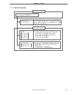
77
Brand: IBM Pages: 12
C6000
Brand: Lauterbach Pages: 67

BLUETOOTH KEYBOARD
Brand: Targus Pages: 7
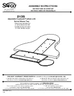
2135
Brand: Safco Pages: 6

ClickShare
Brand: Barco Pages: 7
Action Replay DSi
Brand: Datel Pages: 2
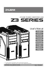
Z3 Series
Brand: ZALMAN Pages: 20
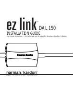
EZ Link DAL 150
Brand: Harman Kardon Pages: 16

Wormhole Station JUH-320
Brand: J5create Pages: 24
FireWire 1814
Brand: M-Audio Pages: 61
iPazzPort
Brand: Unisen Pages: 9
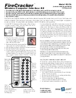
FireCracker CK17A
Brand: X10 Pages: 1
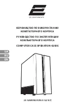
RUNA
Brand: 2E GAMING Pages: 26

NSK 4000
Brand: Antec Pages: 5
EYES 7
Brand: Pout Pages: 5
Dual Shock Rally Master
Brand: Trust Pages: 9
CSAZ-3000
Brand: AZZA Pages: 18
KeyFolio Pro
Brand: Kensington Pages: 82


