background image

Nov. 2003

NEC Corporation

Service manual

68 Cm STEREO Color Television

MODEL : DTE-29U1TH
                 PF-68T32

CHASSIS : CP-785F

S/M No. : TCP785FEF0

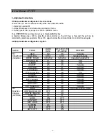
Summary of Contents for DTE-29U1TH

Page 1: ...Nov 2003 NEC Corporation Service manual 68 Cm STEREO Color Television MODEL DTE 29U1TH PF 68T32 CHASSIS CP 785F S M No TCP785FEF0 ...

Page 2: ... TDA835x J Vertical Amplifier 24 4 5 TDA6107JF 26 4 6 24C08 8 K bit EEPROM 27 4 7 STR F665X 28 5 Circuit description 30 5 1 Block diagram 30 5 2 IF 34 5 3 Source switching 35 5 4 Controller I O pin configuration and function 35 5 5 Sound processing 36 5 6 Sound amplification 37 5 7 Vertical deflection 38 5 8 Power supply STR F665X 39 5 9 TV start up TV normal run and stand by mode operations 43 6 ...

Page 3: ...al screen size 68 Cm Channel indicatio On Screen Display Program Selection 100 programmes Aux terminal INPUT1 RCA Audio Video In INPUT2 RCA Audio Video In OUTPUT RCA MONITOR OUT DVD Y Cr Cb Audio in Headphone jack 3 5 mm on the right front of cabinet Remote Control Unit R 44N08 RD D90 for with Teletext Pin Signal Matching value 1 Yellow Video Input 1 0 Vpp 3dB Impedance 75 ohm 2 White Audio Input ...

Page 4: ...75ohm 4 DVD Y in 1Vpp 3dB Impedence 75ohm 5 DVD Audio Left 0 5 Vrms Impedance 10 kohm 6 DVD Audio Right 0 5 Vrms Impedance 10 kohm 7 Monitor Video out 1Vpp 3dB Impedence 75ohm 8 Monitor Audio Left out 0 5Vrms at RF sound FM 54 Mod 27Khz dev 9 Monitor Audio Right out 0 5Vrms at RF sound FM 54 Mod 27Khz dev VIDEO DVD Y Cb L MONO R OUT DVD IN A U D I O Cr 7 4 8 5 9 6 2 3 ...

Page 5: ... 175 25 C07 182 25 C08 189 25 C09 196 25 C10 209 25 C11 216 75 N01 45 25 N02 55 25 N03 62 25 N08 203 25 N09 210 25 N10 217 25 C21 471 25 C22 479 25 C23 487 25 C24 495 25 C25 503 25 C26 511 25 C27 519 25 C28 527 25 C29 534 25 C30 541 25 C31 548 25 C32 555 25 C33 562 25 C34 569 25 C35 576 25 C36 583 25 C37 590 25 C38 597 25 C39 603 25 C40 610 25 C41 617 25 C42 624 25 ...

Page 6: ...52 694 25 C53 701 25 C54 708 25 C55 715 25 C56 722 25 C57 729 25 C58 736 25 C59 743 25 C60 750 25 C61 757 25 C62 764 25 C63 771 25 C64 779 25 C65 786 25 C66 793 25 C67 800 25 C68 807 25 C69 814 25 C70 C71 C72 C73 C74 C75 C76 C77 S01 105 25 S02 112 25 S03 119 25 S04 126 25 S05 133 25 S06 140 25 S07 147 25 S08 154 25 S09 161 25 S10 168 25 S11 231 25 ...

Page 7: ... 25 S16 266 25 S17 273 25 S18 280 25 S19 287 25 S20 294 25 S21 303 25 S22 311 25 S23 319 25 S24 327 25 S25 335 25 S26 343 25 S27 351 25 S28 359 25 S29 367 25 S30 375 25 S31 383 25 S32 391 25 S33 399 25 S34 407 25 S35 415 25 S36 423 25 S37 431 25 S38 439 25 S39 447 25 S40 455 25 S41 463 25 ...

Page 8: ...ent 2 Discharge the high potential of the picture tube before handling the tube The picture tube is highly evacuated and if broken glass fragments will be violently expelled 2 If any Fuse in this TV receiver is blown replace it with the FUSE specified in the Replacement Parts List 3 When replacing a high wattage resistor oxide metal film resistor in circuit board keep the resistor 10 mm away from ...

Page 9: ...the set again Section ITEMS BARE DTE 29U1TH REMARK DATA PF 68T32 For AGC 32 23 Variable Adjustment BIAS R G 31 31 31 31 Variable Variable Variable DRIVE R G B 32 32 32 32 32 32 Variable Variable FIX H PARALLEL 31 26 FIX H BOW 42 34 FIX H SHIFT 25 33 Variable V SLOPE 32 31 Variable V Amplitude 39 20 Variable V S Correction 13 29 FIX V SHIFT 32 30 Variable H WIDTH 32 42 Variable EW Parabola 32 23 Va...

Page 10: ...x Vol 00 43 max this is the limited Volume function it is variable to 43 max from 00 min Clock Pr it change the reference channel for Automatic clock setting SVHS ON OFF When SVHS is active The AV mode is changed to SVHS mode CP 785F can t operate the S VHS It operate to the CP 785A DTE 29 25G5TH AV START ON OFF When AV start is active the set always start in av1 mode main AC switch on off remote ...

Page 11: ...ure and adjust Black G and Black R to the desired colour temperature Select a bright picture and adjust WP Red WP Green WP Blue to the desired colour temperature 3 3 3 Focus Adjust the Focus volume on FBT to have the best resolution on screen 3 3 4 Vertical geometry Adjust the Vertical Amplitude Shift S Correction and Slope to compensate for vertical distortion 3 3 5 Horizontal picture centering A...

Page 12: ... Manual CP 785F 3 3 7 AGC Adjust the antenna signal level at 68 dBV 2 UHF CH25 Set RF AGC to 0 Increase RF AGC level and stop when the level on pin 6 of TDA936x goes below 2 5 Vdc H Bow H Width Up Corner Dw Corner ...

Page 13: ...switchable centre frequency Only one reference 12 MHz crystal required for the Controller Teletext and the colour decoder PAL NTSC or multistandard colour decoder with automatic search system Internal base band delay line RGB control circuit with Continuous Cathode Calibration white point and black level off set adjustment so that the colour temperature of the dark and the bright parts of the scre...

Page 14: ... between 525 WST 625 WST Automatic selection between 625 WST VPS on line 16 of VBI Real time capture and decoding for WST Teletext in Hardware to enable optimised processor throughput Automatic detection of FASTEXT transmission Real time packet 26 engine in Hardware for processing accented G2 and G3 characters Signal quality detector for video and WST VPS data types Comprehensive teletext language...

Page 15: ...covered data and clock the following data types are extracted WST Teletext 625 525 Closed Caption VPS WSS The extracted data is stored in either memory DRAM via the Memory Interface or in SFR locations Data Capture Features Video Signal Quality detector Data Capture for 625 line WST Data Capture for 525 line WST Data Capture for US Closed Caption Data Capture for VPS data PDC system A Data Capture...

Page 16: ... AMP CHROMA PAL SECAM NTSC DECODER H V SYNC SEP H OSC PLL 32 30 41 18 39 14 19 17 H 34 16 33 25 26 22 21 36 20 46 47 48 45 50 49 53 52 51 BLKIN BCLIN BO GO RO COR CONTR BRIGHTN OSD TEXT INSERT CCC WHITE P ADJ HOUT V DRIVE EHTO EWD R V Y R R V H G G B B BL RGB YUV INSERT RGB YUV MATRIX SATURATION YUV RGB MATRIX U V G Y B U BL V V DRIVE GEOMETRY ROM RAM CVBS I 2 C BUS TRANSCEIVER VST PWM DAC I O PRO...

Page 17: ...ply of TV processor PH2LF 16 phase 2 filter PH1LF 17 phase 1 filter GND3 18 ground 3 for TV processor DECBG 19 bandgap decoupling AVL EWD 20 East West drive output VDRB 21 vertical drive B output VDRA 22 vertical drive A output IFIN1 23 IF input 1 IFIN2 24 IF input 2 IREF 25 reference current input VSC 26 vertical sawtooth capacitor TUNERAGC 27 tuner AGC output SIFIN1 28 SIF input 1 SIFIN2 29 SIF ...

Page 18: ...DDA 54 analog supply of Teletext decoder and digital supply of TV Processor 3 3V VPE 55 OTP programming supply VDDC 56 digital supply to core 3 3V OSCGND 57 oscillator ground supply XTALIN 58 crystal oscillator input XTALOUT 59 crystal oscillator output RESET 60 reset VDDP 61 digital supply to periphery 3 3V Audio Mute 62 Port 1 0 Audio mute output PushPull Power 63 Port 1 1 Power output PushPull ...

Page 19: ... SNDPLL SIFAGC AVL REFO AMOUT P1 2 INT0 P1 1 T0 P1 0 INT1 VDDP RESET XTALOUT XTALIN OSCGND VDDC VPE VDDA BO GO RO BLKIN BCLIN B2 UIN G2 YIN R2 VIN INSSW2 AUDOUT AMOUT CHROMA CVBS Y GND1 CVBSINT VP1 IFVO SVO PLLIF EHTO AUDEXT QSSO AMOUT FBISO HOUT 1 2 3 4 5 6 7 8 9 10 11 12 13 14 15 16 17 18 19 20 21 22 23 24 25 26 27 28 29 30 31 32 64 63 62 61 60 59 58 57 56 55 54 53 52 51 50 49 48 47 46 45 44 43 ...

Page 20: ...ion Reduction of necessary controlling Less external components Basic Features of the MSP 341x Demodulator and NICAM Decoder Section The MSP 341x is designed to simultaneously perform digital demodulation and decoding of NICAM coded TV stereo sound as well as demodulation of FM or AM mono TV sound Alternatively two carrier FM systems according to the German terrestrial specs can be processed with ...

Page 21: ...tistandard audio IC NICAM plus FM AM Mono According to the British Scandinavian Spanish and French TV standards high quality stereo sound is transmitted digitally The systems allow two high quality digital sound channels to be added to the already existing FM AM channel The sound coding follows the format of the so called Near Instantaneous Companding System NICAM 728 Transmission is performed usi...

Page 22: ...5 FM Stereo PAL Applied B G 5 5 5 85 FM Mono NICAM PAL Applied L 6 5 5 85 AM Mono NICAM SECAM L N A I 6 0 6 552 FM Mono NICAM PAL N A D K 6 5 6 2578125 D K1 FM Stereo SECAM East 6 5 6 7421875 D K2 N A 6 5 5 85 D K NICAM FM Mono NICAM Architecture of MSP3415D Pin connections and short description Pin No Pin Name Type Short description 1 TP Out Test pin 2 NC Not Connected 3 NC Not Connected 4 TP Out...

Page 23: ...RF Out Right 37 RF_OUT_L Out RF Out Left 38 NC Not Connected 39 AHVSUP Analog power supply 8 0V 40 CAPL_M Volume capacitor MAIN 41 AHVSS Analog ground 42 AGNDC Analog reference voltage high voltage part 43 NC Not Connected 44 NC Not Connected 45 NC Not Connected 46 DVD_In_L In DVD In Left 47 DVD_In_R In DVD In Right 48 ASG2 Analog Shield Ground 2 49 AV_IN_L In AV input 2 in left 50 AV_IN_R In AV i...

Page 24: ...current High supply voltage ripple rejection Outputs short circuit protected to ground supply and across the load Thermally protected Pin description Pin Symbol Description 1 OUT negative loudspeaker terminal 1 2 GND1 ground channel 1 3 Vcc1 supply voltage channel 1 4 OUT1 positive loudspeaker terminal 1 5 n c not connected 6 IN1 positive input1 7 n c not connected 8 IN1 negative input1 9 IN2 nega...

Page 25: ...e in 90 and 110 colour deflection systems for field frequencies of 25 to 200Hz and 16 9 picture tubes The circuit provides a DC driven vertical deflection output circuit operating as a highly efficient class G system Due to the full bridge output circuit the deflection coils can be DC coupled The IC is constructed in a Low Voltage DMOS process that combines Bipolar CMOS and DMOS devices MOS transi...

Page 26: ... the vertical flyback switch Guard circuit Temperature thermal protection High EMC because of common mode inputs East West output stage Vi pos Vi neg Vp VoB View GNDv GNDEW VoEW Vfb VoA Vo guard F back Icomp 1 2 3 4 5 6 7 8 9 10 11 12 13 TDA8358J Icomp V0 guard Vp 9 3 M5 D3 D2 10 M2 M4 M1 5 2 Vi diff Vi sb Vi diff Vi diff Vi sb Vi diff IiEW top IiEW bot Vi neg 1 M4 input feedback Vi neg Vi pos M3 ...

Page 27: ...put signal of 60 Vpp High slew rate of 900V s No external components required Very simple application Single supply voltage of 200V Internal reference voltage of 2 5 V Fixed gain of 50 Black current stabilisation BCS circuit Thermal protection Pin description Pin Symbol Description 1 Vi 1 inverting input 1 2 Vi 2 inverting input 2 3 Vi 3 inverting input 3 4 GND ground fin 5 Iom black current measu...

Page 28: ... Pin description Pin No Name Description 1 2 3 E0 E1 E2 Device address 5 SDA Serial Data Address Input Output 6 SCL Serial clock 7 WC Write contro 8 Vcc Supply voltage 4 Vss Ground The memory device is compatible with the I2C memory standard This is a two wire serial interface that uses a bi directionnal data bus and serial clock The memory carries a built in 4 bit unique device type identifier co...

Page 29: ... S Vth1 0 73 0 05V 4 7 STR F665X 4 7 1 General description The STR F665X is an hybrid IC with a build in MOSFET and control IC designed for flyback converter type switch mode power supply applications 4 7 2 Features Small SIP fully isolated molded 5 pins package Many protection functions Pulse by pulse overcurrent protection OCP Overvoltage protection with latch mode OVP Thermal protection with la...

Page 30: ... TOFF max 45 55 sec Minimum time for input of quaxi 1 5 TTH 2 1 0 sec resonant signals Minimum off time TOFF min 1 5 sec O C P F B terminal threshold 1 5 VTH 1 0 68 0 73 0 78 V voltage 1 O C P F B terminal threshold 1 5 VTH 2 1 3 1 45 1 6 V voltage 2 O C P F B terminal extraction 1 2 IOCP FB 1 2 1 35 1 5 mA current O V P operation voltage 4 5 VIN OVP 20 5 22 5 24 5 V Latch circuit sustaining volta...

Page 31: ...6 53 47 33 34 58 SIF 5 5MHz for system B G Audio out scart 1 Audio in Audio in Audio in Trap 5 5MHz video in 51 46 40 38 35 42 52 47 53 2 3 4 I501 24 23 29 28 Micro controller Video IF IF IF 38 9 MHz All standard except L 33 9 MHz L Audio IF SF1 SF2 Video processor I501 48 video out QSS out ext video in Video in AV 1 AV 2 DVD Y Switching IC RGB out To CRT board DVD in chroma in I602 ...

Page 32: ...deo signals With this system a high performance hi fi stereo sound processing can be achieved Video switches The video switch has one input for an external CVBS The selected CVBS signal can be supplied to pin 38 the IF video output The video ident circuit is connected to the selected signal This ident circuit is independent of the synchronisation Synchronisation circuit The IC contains separator c...

Page 33: ...e crystals but has an internal clock generator which is stabilised to the required frequency by using the 12 MHz clock signal from the reference oscillator of the Controller Teletext decoder The Automatic Colour Limiting ACL circuit switchable via the ACL bit in subaddress 2OH prevents that oversaturation occurs when signals with a high chroma to burst ratio are received The ACL circuit is designe...

Page 34: ...als and nominal settings of the various controls To obtain an accurate biasing of the picture tube the Continuous Cathode Calibration system has been included in these ICs A black level off set can be made with respect to the level which is generated by the black current stabilisation system In this way different colour temperatures can be obtained for the bright and the dark part of the picture T...

Page 35: ...is tuned using the direct frequency entry or after fine tuning adjustment Therefore it is recommended to tune channel with the TV search function manual or Auto setup or using the direct channel entry to enable the Automatic Frequency Control SAW filters Ref Standard Features K3953M B G IF filter for video application TV IF filter with Nyquist slopes at 38 9 MHz Constant group delay K9650M B G IF ...

Page 36: ...switching is done in the MSP341XD I601 by the Controller via I2C bus 5 4 Controller I O pin configuration and function The I O pins of the Controller can be configured in many way All port functions can be individually programmed by use of the SFR registers Each I O port pin can be individually programmed in these configurations Open drain In this mode the port can function as in and output It req...

Page 37: ...ance Open Drain 11 Green LED Open Drain High impedance 62 Audio mute Push Pull Push Pull High in stand by mode 5 5 Sound processing Analogue sound IF input section The input pins ANA_IN1 and ANA_IN offer the possibility to connect sound IF sources to the MSP 3415D The analogue to digital conversion of the preselected sound IF signal is done by an A D converter whose output is used to control an an...

Page 38: ... 1 if the transmission quality is too poor To avoid unwanted automatic switching the threshold levels mono to stereo and stereo to mono is different In forced mono mode Red OSD in recall section the controlling software configure the MSP3415D to demodulate only the analogue FM or AM sound carrier 1 no matter the signal quality The sound mode forced or Autodetect is stored for each programme 5 6 So...

Page 39: ...al feedback information The voltage across R302 is proportional to the output current Flyback voltage The flyback voltage is determined by an additional supply voltage Vflb The principle of operation with two supply voltages class G makes it possible to fix the supply voltage Vp optimum for the scan voltage and the second supply voltage Vflb optimum for the flyback voltage Using this method very h...

Page 40: ...Power supply primary part operations An oscillator generates pulses signals which turn on and off a MOSFET transistor Start up circuit VIN The start up circuit is used to start and stop the operation of the control IC by detecting a voltage appearing at VIN pin pin 4 R819 D802 D801 D803 D804 C804 C803 R802 C806 C805 Main AC voltage 2 D805 R805 L801 4 Ground Drain Vin T801 SMPS TRANS 3 I801 STR F66...

Page 41: ...ely after the control circuit starts operating VIN starts dropping However as this winding voltage reaches the set value before VIN voltage drops to the shutdown voltage at 11V the control circuit continues operating see below VIN voltage at start up R805 resistor prevents that VIN pin voltage varies according to the secondary side output current VIN must be set higher than the shutdown voltage VI...

Page 42: ...Comp 1 C1 R1 STR F665X 1 35mA V th 1 V th 2 Oscillating operation O N O N O N O F F O F F O F F M O S F E T s w i t c h i n g O N O F F V D S M O S F E T d r a i n s o u r c e v o l t a g e I D M O S F E T d r a i n c u r r e n t P i n 1 O C P F B 0 V 0 7 3 V S T R F 6 6 5 3 i n t e r n a l c a p a c i t o r C 1 3 7 V 6 5 V 1 3 2 4 Waveforms during oscillating operation ...

Page 43: ...termined by C1 and R1 is the OFF time of the MOSFET When C1 voltage falls to around 3 7V the STR F665X internal oscillator is reversed again and the MOSFET turns ON C1 is quickly charged to around 6 5V The MOSFET continues to oscillate by repeating the above procedure STR F665X protection circuits overcurrent protection function OCP Overcurrent protection is performed pulse by pulse detecting at S...

Page 44: ...oltage is applied to T801 transformer after rectification by D801 D804 diodes Then T801 SMPS transformer starts operating and supplies DC voltage to I823 3 3V regulator This regulator provides 3 3V DC voltage to I501 microcontroller power supply pins pins 54 56 61 and to the reset pulse circuit which provides reset pulse to I501 microcontroller reset pin pin 60 Then the microcontroller starts its ...

Page 45: ...he microcontroller delivers horizontal drive voltage at pin 33 and picture appears on screen If the TV set was on stand by mode before switching off the microcontroller switches TV set to stand by mode decreasing power pin voltage pin 63 This matter will be explained on paragraph 5 9 2 b ...

Page 46: ...mode I501 microcontroller part pin 63 power effect I501 microcontroller part pin 63 power is connected to the following circuit I 8 1 0 C O N T R O L L E D R E C T I F I E R R 8 2 0 R 8 3 0 C 8 3 0 R 8 2 9 Q 8 0 8 6 V D C 1 1 V D C R 8 7 0 D 8 1 1 Q 8 1 1 Q 8 0 9 Q 8 0 7 Q 8 1 0 L O W L O W L O W L O W H I G H H I G H C O N D U C T I N G P O W E R H I G H N O T C O N D U C T I N G I501 microcontro...

Page 47: ...om Q810 collector to the ground Therefore the power supply circuit diagram is the one shown on the next paragraph power supply circuit diagram during TV set normal run I 8 2 0 5 V R E G U L A T O R I 8 2 3 3 3 V R E G U L A T O R I602 3 16 TDA894X 5 V 3 3 V 3 3 1 1 1 1 V 8 V 6 V 1 3 1 4 3 V C P 7 8 5 D 8 2 0 D 8 6 0 D 8 3 0 D 8 3 1 C 8 3 2 C 8 2 3 C 8 6 1 1 2 1 4 1 5 1 8 2 4 C 8 1 3 R 8 2 3 R 8 1 ...

Page 48: ...required on this line 143V supply voltage line includes an IC error amplifier I806 which corrects unexpected DC voltage variations on this line power supply IC delivery during TV set normal run power supply line IC power supply delivery Remarks FBT supplies 55V to I301 vertical IC FBT supplies 55V to T401 H drive 143V FBT FBT supplies 14V to I301 vertical IC FBT supplies 33V to the tuner FBT suppl...

Page 49: ...S TRA N S I501 M A I N IC OCP FB 16 D821 I810 controlled rectifier HIGH C841 C840 R713 1 3 1 2 61 64 56 54 7 63 CONDUCTING I R I N µ com supply voltage K E Y I N POWER R888 C888 Q809 Q810 Q811 D811 D825 R810 L801 D806 C808 SW801 POWER SWITCH C850 R806 8 4 3 1 2 R870 HIGH LOW LOW CONDUCTING CONDUCTING AROUND 6V dc AROUND 3 3Vdc Power supply operation in stand by mode D801 D804 GRAETZ BRIDGE b TV se...

Page 50: ...ier gate pin is set to high and I810 is conducting So current flows from pin 16 SMPS transformer to the ground via I804 optocoupler and Q810 and Q811 transistors which are conducting In these conditions I801 delivers pulses on light mode and T801 produces voltages with reduced power As I810 is conducting current flows also from pin 16 SMPS transformer to I823 3 3V regulator for I501 com IR receive...

Page 51: ...S PTFMSJK016 DTE 29U1 P601A CONNECTOR 4850704S32 YH025 04 YRT205 ULW900500 SP01 SPEAKER 4858311110 12W 8 OHM SP 58126F SP02 SPEAKER 4858311110 12W 8 OHM SP 58126F ZZ290 PCB MAIN MANUAL AS PTMPMSD913 DTE 29U1TH ZZ300 PCB UNION AS PTUNSWD913 DTE 29U1TH is safety component so it must be used the same component is a recommendable part for stock In this Manual some parts can be changed for improving th...

Page 52: ...PF J C408 C MYLAR CMYE2G394J 400V PU 0 39MF J C409 C CERA CXCH2H470J 500V CH 47PF J TAPPING C412 C ELECTRO CEXF2C339C 160V RUS 3 3MF 8X11 5 TP C414 C MYLAR CMXM2A104J 100V 0 1MF J TP C418 C CERA CCXB1H102K 50V B 1000PF K TAPPING C420 C CERA CCXB2H222K 500V B 2200PF K TAPPING C430 C MYLAR CMXH3C122J 1 6KV BUP 1200PF J TP C431 C MYLAR CMXE2D103J 200V PU 0 01MF J TP C440 C MYLAR CMXE2G273J 400V PU 0 ...

Page 53: ...ECTRO CEXF1H229V 50V RSS 2 2MF 5X11 TP C555 C ELECTRO CEXF1C470V 16V RSS 47MF 5X11 TP C560 C CERA SEMI CBXF1H104Z 50V F 0 1MF Z TAPPING C561 C ELECTRO CEXF1E101V 25V RSS 100MF 6 3X11 TP C564 C ELECTRO CEXF1E101V 25V RSS 100MF 6 3X11 TP C565 C CERA SEMI CBXF1H104Z 50V F 0 1MF Z TAPPING C577 C CERA CCXB1H561K 50V B 560PF K TAPPING C585 C CERA CCXB1H222K 50V B 2200PF K TAPPING C590 C CERA CXCH1H270J ...

Page 54: ...C472M 16V Y5R 4700PF M AXIAL C668 C MYLAR CMXL1J224J 63V MEU 0 22MF J TP C669 C MYLAR CMXL1J224J 63V MEU 0 22MF J TP C698 C CERA CXCH1H470J 50V CH 47PF J TAPPING C699 C CERA CXCH1H470J 50V CH 47PF J TAPPING C770 C ELECTRO CEXF1E101V 25V RSS 100MF 6 3X11 TP C771 C CERA SEMI CBXF1H104Z 50V F 0 1MF Z TAPPING C801 C LINE ACROSS CL1UC3474M 0 47MF 1J UCVSNDF SV Q O C803 C CERA CCXF3A472Z 1KV F 4700PF Z ...

Page 55: ...R DUZ33B UZ 33B D381 DIODE ZENER DUZ33B UZ 33B D403 DIODE DDGP30L DGP30L D404 DIODE DRGP15J RGP15J DO 204AC 600V 1 5A D405 DIODE D1N4937G 1N4937G TAPPING D406 DIODE DRGP15J RGP15J DO 204AC 600V 1 5A D407 DIODE D1N4937G 1N4937G TAPPING D408 DIODE D1N4937G 1N4937G TAPPING D410 DIODE D1N4004S 1N4004S D411 DIODE D1N4004S 1N4004S D450 DIODE D1N4937G 1N4937G TAPPING D520 DIODE D1N4148 1N4148 TAPPING D52...

Page 56: ...9 EYE LET 4856310300 BSR T0 2 R1 6 E010 EYE LET 4856310300 BSR T0 2 R1 6 E011 EYE LET 4856310600 BSR T0 2 R2 3 E012 EYE LET 4856310600 BSR T0 2 R2 3 E013 EYE LET 4856310600 BSR T0 2 R2 3 E014 EYE LET 4856310600 BSR T0 2 R2 3 E015 EYE LET 4856310600 BSR T0 2 R2 3 E016 EYE LET 4856310600 BSR T0 2 R2 3 E017 EYE LET 4856310300 BSR T0 2 R1 6 E018 EYE LET 4856310600 BSR T0 2 R2 3 E019 EYE LET 4856310300...

Page 57: ...0 2 R1 6 E069 EYE LET 4856310300 BSR T0 2 R1 6 E077 EYE LET 4856310300 BSR T0 2 R1 6 E078 EYE LET 4856310300 BSR T0 2 R1 6 E079 EYE LET 4856310300 BSR T0 2 R1 6 E116 EYE LET 4856310600 BSR T0 2 R2 3 E118 EYE LET 4856310600 BSR T0 2 R2 3 F801 FUSE 5FWPS4022L WIDE TL 250V 4A CASE FUSE GLASS TUBE 5FSGB4022L SEMKO TL 4A 250V MF51 COMPATIBLE F801A CLIP FUSE 4857415001 PFC5000 0702 WHEN 5FSGB4022L IS US...

Page 58: ...G J016 WIRE COPPER 85801065GY AWG22 1 0 65 TIN COATING J017 WIRE COPPER 85801065GY AWG22 1 0 65 TIN COATING J018 WIRE COPPER 85801065GY AWG22 1 0 65 TIN COATING J019 WIRE COPPER 85801065GY AWG22 1 0 65 TIN COATING J020 WIRE COPPER 85801065GY AWG22 1 0 65 TIN COATING J021 WIRE COPPER 85801065GY AWG22 1 0 65 TIN COATING J022 WIRE COPPER 85801065GY AWG22 1 0 65 TIN COATING J023 WIRE COPPER 85801065GY...

Page 59: ...1065GY AWG22 1 0 65 TIN COATING J063 WIRE COPPER 85801065GY AWG22 1 0 65 TIN COATING J064 WIRE COPPER 85801065GY AWG22 1 0 65 TIN COATING J065 WIRE COPPER 85801065GY AWG22 1 0 65 TIN COATING J066 WIRE COPPER 85801065GY AWG22 1 0 65 TIN COATING J067 WIRE COPPER 85801065GY AWG22 1 0 65 TIN COATING J068 WIRE COPPER 85801065GY AWG22 1 0 65 TIN COATING J069 WIRE COPPER 85801065GY AWG22 1 0 65 TIN COATI...

Page 60: ...0 65 TIN COATING JPA1 JACK PIN BOARD 4859109250 PH JB 9614A JPA3 JACK PIN BOARD 4859111750 PH JB 9515 L101 COIL PEAKING 5CPZ100K02 10UH K AXIAL 3 5MM L350 COIL PEAKING 5CPZ109M04 1UH 10 5MM M LAL04TB L381 COIL PEAKING 5CPZ109M04 1UH 10 5MM M LAL04TB L401 COIL H LINEARITY 58H0000047 TRL 190D L402 COIL CHOKE 58C7070085 TLN 3062A L500 COIL PEAKING 5CPZ120K02 12UH K AXIAL 3 5MM L501 COIL PEAKING 5CPZ1...

Page 61: ... TR TKTA1266Y KTA1266Y TP Q807 TR TKTC3198Y KTC3198Y Q808 TR TKTC3198Y KTC3198Y Q809 TR TKTC3198Y KTC3198Y Q810 TR TKTC3198Y KTC3198Y Q811 TR TKTC3198Y KTC3198Y Q822 TR TKTC3205Y KTC3205Y TP R101 R CARBON FILM RD AZ473J 1 6 47K OHM J R102 R CARBON FILM RD AZ472J 1 6 4 7K OHM J R103 R CARBON FILM RD AZ123J 1 6 12K OHM J R104 R CARBON FILM RD AZ104J 1 6 100K OHM J R105 R CARBON FILM RD AZ392J 1 6 3 ...

Page 62: ...CARBON FILM RD AZ101J 1 6 100 OHM J R506 R CARBON FILM RD AZ332J 1 6 3 3K OHM J R507 R CARBON FILM RD AZ101J 1 6 100 OHM J R508 R CARBON FILM RD AZ332J 1 6 3 3K OHM J R509 R CARBON FILM RD AZ681J 1 6 680 OHM J R512 R CARBON FILM RD AZ101J 1 6 100 OHM J R513 R CARBON FILM RD AZ101J 1 6 100 OHM J R515 R CARBON FILM RD AZ153J 1 6 15K OHM J R516 R CARBON FILM RD AZ393J 1 6 39K OHM J R517 R CARBON FILM...

Page 63: ... 1 6 220K OHM J R586 R CARBON FILM RD AZ221J 1 6 220 OHM J R597 R METAL FILM RN 4Z1502F 1 4 15K OHM F R598 R METAL FILM RN 4Z1502F 1 4 15K OHM F R599 R CARBON FILM RD AZ101J 1 6 100 OHM J R605 R CARBON FILM RD AZ751J 1 6 750 OHM J R606 R CARBON FILM RD AZ751J 1 6 750 OHM J R610 R CARBON FILM RD AZ102J 1 6 1K OHM J R611 R CARBON FILM RD AZ104J 1 6 100K OHM J R620 R CARBON FILM RD AZ752J 1 6 7 5K OH...

Page 64: ...220J 1 4 22 OHM J R841 R CARBON FILM RD 2Z479J 1 2 4 7 OHM J R842 R CARBON FILM RD 2Z479J 1 2 4 7 OHM J R843 R CARBON FILM RD AZ561J 1 6 560 OHM J R844 WIRE COPPER 85801065GY AWG22 1 0 65 TIN COATING R850 R CARBON FILM RD 2Z479J 1 2 4 7 OHM J R855 R CARBON FILM RD 4Z185J 1 4 1 8M OHM J R870 R CARBON FILM RD 2Z222J 1 2 2 2K OHM J R888 R CARBON FILM RD AZ103J 1 6 10K OHM J R910 R CARBON FILM RD AZ10...

Page 65: ... R CARBON FILM RD AZ750J 1 6 75 OHM J RA11 R CARBON FILM RD AZ750J 1 6 75 OHM J RA16 R CARBON FILM RD AZ910J 1 6 91 OHM J RA40 R CARBON FILM RD AZ102J 1 6 1K OHM J RA41 R CARBON FILM RD AZ102J 1 6 1K OHM J SCT1 SOCKET CRT 4859303530 PCS629 03C 48592303830 ISMG94S COMPATIBLE SD2 RETA PCB 4853747800 NYLON 66 SF01 FILTER SAW 5PK3953M K3953M SF02 FILTER SAW 5PK9650M K9650M SW700 SW TACT 5S50101090 THV...

Page 66: ...ZSL1H470J 50V SL 47PF J CXCH1H470J 50V CH 47PF J C CERA C771 C830 CBZF1H104Z 50V F 0 1MF Z CBXF1H104Z 50V F 0 1MF Z C CERA C809 CCZB1H102K 50V B 1000PF K CCXB1H102K 50V B 1000PF K C CERA C665 C667 CCXB1H472K 50V B 4700PF K CBZR1C472M 16V Y5R 4700PF M DIODE ZENER D360 and more 1UPC574J UPC574J DUZ33B UZ 33B DIODE D403 DDG3 DG3 DDGP30L DGP30L Diode Maker s Package change IC REGULATOR I820 1K1A7805P1...

Page 67: ...Service Manual CP 785F 66 7 Exploded view ...

Page 68: ...Service Manual CP 785F 67 8 PCB Layout 8 1 Main PCB ...

Page 69: ...Service Manual CP 785F 68 8 2 AV PCB ...

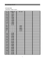
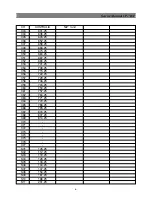
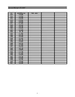
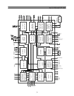
Page 70: ... 69 Service Manual CP 785F 9 Circuit Diagram ...

Page 71: ...NEC Corporation 7 1 SHIBA 5 CHOME MINATO KU TOKYO 108 8001 JAPAN ...

Reviews: