background image

User’s Manual

Common to 78K/0S Series

78K/0S Series

8-Bit Single-Chip Microcontroller

Instructions

Printed in Japan

Document No.

U11047EJ3V0UMJ1 (3rd edition)

Date Published November 2000 N  CP(K)

1996

©

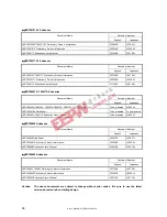
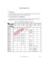
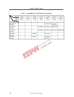
Summary of Contents for 78K/0S Series

Page 1: ...User s Manual Common to 78K 0S Series 78K 0S Series 8 Bit Single Chip Microcontroller Instructions Printed in Japan Document No U11047EJ3V0UMJ1 3rd edition Date Published November 2000 N CP K 1996 ...

Page 2: ...User s Manual U11047EJ3V0UM00 2 MEMO ...

Page 3: ...aterial All test and measurement tools including work bench and floor should be grounded The operator should be grounded using wrist strap Semiconductor devices must not be touched with bare hands Similar precautions need to be taken for PW boards with semiconductor devices on it 2 HANDLING OF UNUSED INPUT PINS FOR CMOS Note No connection for CMOS device inputs can be cause of malfunction If no co...

Page 4: ...uality reliability and safety of NEC semiconductor products customers agree and acknowledge that the possibility of defects thereof cannot be eliminated entirely To minimize risks of damage to property or injury including death to persons arising from defects in NEC semiconductor products customers must incorporate sufficient safety measures in their design such as redundancy fire containment and ...

Page 5: ...tronics Germany GmbH Duesseldorf Germany Tel 0211 65 03 02 Fax 0211 65 03 490 NEC Electronics UK Ltd Milton Keynes UK Tel 01908 691 133 Fax 01908 670 290 NEC Electronics Italiana s r l Milano Italy Tel 02 66 75 41 Fax 02 66 75 42 99 NEC Electronics Germany GmbH Benelux Office Eindhoven The Netherlands Tel 040 2445845 Fax 040 2444580 NEC Electronics France S A Velizy Villacoublay France Tel 01 30 6...

Page 6: ...156 789167 789177 789197AY 789217AY 789407A 789417A and 789842 Subseries Deletion of the following target products µPD789407 789417 and 789806Y Subseries p 52 Modification of MOV PSW byte instruction code p 52 Modification of MOVW rp AX instruction code p 54 Modification of XOR A r instruction code p 54 Modification of CMP A r instruction code The mark shows major revised points ...

Page 7: ...AY µPD789407A Subseries µPD789405A 789406A 789407A µPD789417A Subseries µPD789415A 789416A 789417A 78F9418A µPD789800 Subseries µPD789800 78F9801 µPD789842 Subseries Note µPD789841 789842 78F9842 Note Under development Purpose This manual is intended for users to understand the instruction functions of 78K 0S Series products Organization The contents of this manual are broadly divided into the fol...

Page 8: ... common to 78K 0S Series Document Number Document Name English Japanese User s Manual Instructions This manual U11047J Individual documents µ µ µ µPD789014 Subseries Document Number Document Name English Japanese µPD789011 789012 Data Sheet U11095E U11095J µPD78P9014 Data Sheet U10912E U10912J µPD789014 Subseries User s Manual U11187E U11187J µ µ µ µPD789026 Subseries Document Number Document Name...

Page 9: ...U13045E U13045J µ µ µ µPD789134 Subseries Document Number Document Name English Japanese µPD789131 789132 789134 Preliminary Product Information U13015E U13015J µPD78F9136 Preliminary Product Information U13036E U13036J µPD789134 Subseries User s Manual U13045E U13045J µ µ µ µPD789146 789156 Subseries Document Number Document Name English Japanese µPD789144 789146 789154 789156 Preliminary Product...

Page 10: ... Japanese µPD789405A 789406A 789407A 789415A 789416A 789417A Data Sheet To be prepared U14024J µPD78F9418A Data Sheet To be prepared To be prepared µPD789407A 789417A Subseries User s Manual To be prepared U13952J µ µ µ µPD789800 Subseries Document Number Document Name English Japanese µPD789800 Data Sheet U12627E U12627J µPD78F9801 Preliminary Product Information U12626E U12626J µPD789800 Subseri...

Page 11: ...ive addressing 29 3 1 2 Immediate addressing 30 3 1 3 Table indirect addressing 31 3 1 4 Register addressing 32 3 2 Addressing of Operand Address 33 3 2 1 Direct addressing 33 3 2 2 Short direct addressing 34 3 2 3 Special function register SFR addressing 35 3 2 4 Register addressing 36 3 2 5 Register indirect addressing 37 3 2 6 Based addressing 38 3 2 7 Stack addressing 38 CHAPTER 4 INSTRUCTION ...

Page 12: ...crement Decrement Instructions 78 5 6 Rotate Instructions 83 5 7 Bit Manipulation Instructions 88 5 8 CALL RETURN Instructions 92 5 9 Stack Manipulation Instructions 97 5 10 Unconditional Branch Instruction 101 5 11 Conditional Branch Instructions 103 5 12 CPU Control Instructions 111 APPENDIX A INSTRUCTION INDEX MNEMONIC BY FUNCTION 117 APPENDIX B INSTRUCTION INDEX MNEMONIC IN ALPHABETICAL ORDER ...

Page 13: ...le 0000H to 002BH µPD789026 Subseries 17 1 4 Vector Table 0000H to 0019H µPD789046 Subseries 17 1 5 Vector Table 0000H to 0015H µPD789104 789114 789124 789134 Subseries 17 1 6 Vector Table 0000H to 0019H µPD789146 789156 Subseries 18 1 7 Vector Table 0000H to 0023H µPD789167 789177 Subseries 18 1 8 Vector Table 0000H to 0027H µPD789197AY 789217AY Subseries 18 1 9 Vector Table 0000H to 0023H µPD789...

Page 14: ...User s Manual U11047EJ3V0UM00 14 MEMO ...

Page 15: ...es 16 Kbytes 24 Kbytes 32 Kbytes Address Space Subseries Name 0000H to 07FFH 0000H to 0FFFH 0000H to 1FFFH 0000H to 2FFFH 0000H to 3FFFH 0000H to 5FFFH 0000H to 7FFFH µPD789014 Subseries µPD789011 µPD789012 µPD78P9014 µPD789026 Subseries µPD789022 µPD789024 µPD789025 µPD789026 µPD78F9026 µPD789046 Subseries µPD789046 µPD78F9046 µPD789104 Subseries µPD789101 µPD789102 µPD789104 µPD789114 Subseries ...

Page 16: ...s Space Subseries Name 0000H to 07FFH 0000H to 0FFFH 0000H to 1FFFH 0000H to 2FFFH 0000H to 3FFFH 0000H to 5FFFH 0000H to 7FFFH µPD789217AY Subseries µPD789216AY µPD789217AY µPD78F9217AY µPD789407A Subseries µPD789405A µPD789406A µPD789407A µPD789417A Subseries µPD789415A µPD789416A µPD789417A µPD78F9418A µPD789800 Subseries µPD789800 µPD78F9801 µPD789842 Subseries µPD789841 µPD789842 µPD78F9842 ...

Page 17: ... µ µ µPD789026 Subseries Vector Table Address Interrupt Request Vector Table Address Interrupt Request 0000H RESET input 000CH INTSR INTCSI0 0004H INTWDT 000EH INTST 0006H INTP0 0010H INTTM0 0008H INTP1 0014H INTTM2 000AH INTP2 002AH INTKR Table 1 4 Vector Table 0000H to 0019H µ µ µ µPD789046 Subseries Vector Table Address Interrupt Request Vector Table Address Interrupt Request 0000H RESET input ...

Page 18: ...t Request Vector Table Address Interrupt Request 0000H RESET input 0012H INTWT 0004H INTWDT 0014H INTWTI 0006H INTP0 0016H INTTM80 0008H INTP1 0018H INTTM81 000AH INTP2 001AH INTTM82 000CH INTP3 001CH INTTM90 000EH INTSR20 INTCSI20 0022H INTAD0 0010H INTST20 Table 1 8 Vector Table 0000H to 0027H µ µ µ µPD789197AY 789217AY Subseries Vector Table Address Interrupt Request Vector Table Address Interr...

Page 19: ...NTWT Table 1 10 Vector Table 0000H to 0019H µ µ µ µPD789800 Subseries Vector Table Address Interrupt Request Vector Table Address Interrupt Request 0000H RESET input 000EH INTUSBRE 0004H INTWDT 0010H INTP0 0006H INTUSBTM 0012H INTCSI10 0008H INTUSBRT 0014H INTTM00 000AH INTUSBRD 0016H INTTM01 000CH INTUSBST 0018H INTKR00 Table 1 11 Vector Table 0000H to 0023H µ µ µ µPD789842 Subseries Vector Table...

Page 20: ...789197AY 789217AY Subseries Electrically erasable PROM EEPROM is allocated in the address space shown in Table 1 12 Unlike ordinary RAM EEPROM retains the data it contains even when the power is turned off Also unlike EPROM the contents of EEPROM can be erased electrically without the need to expose the chip to ultraviolet light Table 1 12 Internal Data Memory Space of 78K 0S Series Products 1 2 S...

Page 21: ...s µPD78F9156 µPD789167 µPD789166 FD00H to FEFFH Subseries µPD789167 512 bytes µPD789177 µPD789176 FD00H to FEFFH Subseries µPD789177 512 bytes µPD78F9177 µPD789197AY µPD789196AY FD00H to FEFFH F800H to F87FH Subseries µPD789197AY 512 bytes 128 bytes µPD78F9197AY µPD789217AY µPD789216AY FD00H to FEFFH F800H to F87FH Subseries µPD789217AY 512 bytes 128 bytes µPD78F9217AY µPD789407A µPD789405A FD00H ...

Page 22: ...CE User s Manual U11047EJ3V0UM00 22 1 6 Special Function Register SFR Area Special function registers SFRs of on chip peripheral hardware are allocated to the area FF00H to FFFFH refer to the User s Manual of each product ...

Page 23: ... data and register contents are set When the ______________ RESET signal is input the program counter is set to the value of the reset vector table which are located at addresses 0000H and 0001H Figure 2 1 Format of Program Counter 15 0 PC15 PC14 PC13 PC12 PC11 PC10 PC9 PC8 PC7 PC6 PC5 PC4 PC3 PC2 PC1 PC0 PC 2 1 2 Program status word PSW Program status word is an 8 bit register consisting of vario...

Page 24: ...t 3 this flag is set 1 otherwise it is reset 0 4 Carry flag CY This flag records an overflow or underflow upon add subtract instruction execution It also records the shift out value upon rotate instruction execution and functions as a bit accumulator during bit operation instruction execution 2 1 3 Stack pointer SP This is a 16 bit register that holds the first address of the stack area in the mem...

Page 25: ...DE and HL Registers can be described in terms of functional names X A C B E D L H AX BC DE and HL and absolute names R0 to R7 and RP0 to RP3 Interrupt PSW PC15 to PC8 PC15 to PC8 PC7 to PC0 Lower byte in register pair SP SP 2 SP 2 CALL CALLT instructions PUSH rp instruction SP 1 SP SP SP 2 SP 2 SP 1 SP PC7 to PC0 SP 3 SP 2 SP 1 SP SP SP 3 Upper byte in register pair RETI instruction PSW PC15 to PC...

Page 26: ...UM00 26 Figure 2 6 General Purpose Register Configuration a Absolute name R0 15 0 7 0 16 bit processing 8 bit processing RP3 RP2 RP1 RP0 R1 R2 R3 R4 R5 R6 R7 b Functional name X 15 0 7 0 16 bit processing 8 bit processing HL DE BC AX A C B E D L H ...

Page 27: ...ction register type The bit unit for manipulation is specified as follows 1 bit manipulation Describes a symbol reserved by the assembler for the 1 bit manipulation instruction operand sfr bit This manipulation can also be specified with an address 8 bit manipulation Describes a symbol reserved by the assembler for the 8 bit manipulation instruction operand sfr This manipulation can also be specif...

Page 28: ...User s Manual U11047EJ3V0UM00 28 MEMO ...

Page 29: ...dressing Function The value obtained by adding the 8 bit immediate data displacement value jdisp8 of an instruction code to the first address of the following instruction is transferred to the program counter PC and program branches The displacement value is treated as signed two s complement data 128 to 127 and bit 7 becomes a sign bit Thus relative addressing causes a branch to an address within...

Page 30: ...to the program counter PC and program branches This function is carried out when the CALL addr16 or BR addr16 instruction is executed The CALL addr16 and BR addr16 instructions can be used to branch to any address within the memory spaces Illustration In case of CALL addr16 or BR addr16 instruction 15 0 PC 8 7 7 0 CALL or BR Low addr High addr ...

Page 31: ...rred to the program counter PC and program branches Table indirect addressing is performed when the CALLT addr5 instruction is executed This instruction references the address stored in the memory table from 40H to 7FH and allows branching to the entire memory space Illustration 15 1 15 0 PC 7 0 Low addr High addr Memory table Effective address 1 Effective address 0 1 0 0 0 0 0 0 0 0 8 7 8 7 6 5 0...

Page 32: ... Register addressing Function Register pair AX contents specified with an instruction word are transferred to the program counter PC and program branches This function is carried out when the BR AX instruction is executed Illustration 7 0 rp 0 7 A X 15 0 PC 8 7 ...

Page 33: ...ecution 3 2 1 Direct addressing Function This addressing directly addresses a memory to be manipulated with immediate data in an instruction word Operand format Operand Description addr16 Label or 16 bit immediate data Description example MOV A FE00H When setting addr16 to FE00H Instruction code 0 0 1 0 1 0 0 1 OP code 0 0 0 0 0 0 0 0 00H 1 1 1 1 1 1 1 0 FEH Illustration 7 0 OP code addr16 lower M...

Page 34: ...re register of the timer event counter are mapped and these SFRs can be manipulated with a small number of bytes and clocks When 8 bit immediate data is 20H to FFH bit 8 of an effective address is set to 0 When it is 00H to 1FH bit 8 is set to 1 See Illustration below Operand format Operand Description saddr Label or FE20H to FF1FH immediate data saddrp Label or FE20H to FF1FH immediate data even ...

Page 35: ...d This addressing is applied to the 240 byte spaces of FF00H to FFCFH and FFE0H to FFFFH However the SFRs mapped at FF00H to FF1FH can also be accessed by means of short direct addressing Operand format Operand Description sfr Special function register name Description example MOV PM0 A When selecting PM0 for sfr Instruction code 1 1 1 0 0 1 1 1 0 0 1 0 0 0 0 0 Illustration 15 0 SFR Effective addr...

Page 36: ... executed When an 8 bit register is specified one of the eight registers is specified with 3 bits register specification code in the instruction code Operand format Operand Description r X A C B E D L H rp AX BC DE HL r and rp can be described with absolute names R0 to R7 and RP0 to RP3 as well as functional names X A C B E D L H AX BC DE and HL Description example MOV A C When selecting the C reg...

Page 37: ...ssed is specified with the register pair specification code in an instruction code This addressing can be carried out for the entire memory space Operand format Operand Description DE HL Description example MOV A DE When selecting register pair DE Instruction code 0 0 1 0 1 0 1 1 Illustration 15 0 8 D 7 E 0 7 7 0 A DE Memory address specified with register pair DE The contents of the specified mem...

Page 38: ...y space Operand format Operand Description HL byte Description example MOV A HL 10H When setting byte to 10H Instruction code 0 0 1 0 1 1 0 1 0 0 0 1 0 0 0 0 3 2 7 Stack addressing Function This addressing is to indirectly address the stack area with the stack pointer SP contents This addressing method is automatically employed when the PUSH POP subroutine call or RETURN instructions is executed o...

Page 39: ...User s Manual U11047EJ3V0UM00 39 CHAPTER 4 INSTRUCTION SET This chapter lists the instruction set of the 78K 0S Series The instructions are common to all 78K 0S Series products ...

Page 40: ...ure to describe or For operand register description formats r and rp either functional names X A C etc or absolute names names in parentheses in the table below R0 R1 R2 etc can be described Table 4 1 Operand Representation and Description Formats Operand Description Format r rp sfr X R0 A R1 C R2 B R3 E R4 D R5 L R6 H R7 AX RP0 BC RP1 DE RP2 HL RP3 Special function register symbol saddr saddrp FE...

Page 41: ...ord CY Carry flag AC Auxiliary carry flag Z Zero flag IE Interrupt request enable flag NMIS Non maskable interrupt servicing flag Memory contents indicated by address or register contents in parentheses XH XL Higher 8 bits and lower 8 bits of 16 bit register Logical product AND Logical sum OR Exclusive logical sum exclusive OR Inverted data addr16 16 bit immediate data or label jdisp8 Signed 8 bit...

Page 42: ...1 4 Description of clock column The number of clock cycles during instruction execution is outlined as follows One instruction clock cycle is equal to one CPU clock cycle fCPU selected by the processor clock control register PCC The operation list is shown below ...

Page 43: ...fr A 2 4 sfr A A addr16 3 8 A addr16 addr16 A 3 8 addr16 A PSW byte 3 6 PSW byte A PSW 2 4 A PSW PSW A 2 4 PSW A A DE 1 6 A DE DE A 1 6 DE A A HL 1 6 A HL HL A 1 6 HL A A HL byte 2 6 A HL byte HL byte A 2 6 HL byte A XCH A X 1 4 A X A r Note 2 2 6 A r A saddr 2 6 A saddr A sfr 2 6 A sfr A DE 1 8 A DE A HL 1 8 A HL A HL byte 2 8 A HL byte Notes 1 Except r A 2 Except r A X Remark One instruction clo...

Page 44: ... A HL 1 6 A CY A HL A HL byte 2 6 A CY A HL byte ADDC A byte 2 4 A CY A byte CY saddr byte 3 6 saddr CY saddr byte CY A r 2 4 A CY A r CY A saddr 2 4 A CY A saddr CY A addr16 3 8 A CY A addr16 CY A HL 1 6 A CY A HL CY A HL byte 2 6 A CY A HL byte CY SUB A byte 2 4 A CY A byte saddr byte 3 6 saddr CY saddr byte A r 2 4 A CY A r A saddr 2 4 A CY A saddr A addr16 3 8 A CY A addr16 A HL 1 6 A CY A HL ...

Page 45: ...r16 A HL 1 6 A A HL A HL byte 2 6 A A HL byte OR A byte 2 4 A A byte saddr byte 3 6 saddr saddr byte A r 2 4 A A r A saddr 2 4 A A saddr A addr16 3 8 A A addr16 A HL 1 6 A A HL A HL byte 2 6 A A HL byte XOR A byte 2 4 A A byte saddr byte 3 6 saddr saddr byte A r 2 4 A A r A saddr 2 4 A A saddr A addr16 3 8 A A addr16 A HL 1 6 A A HL A HL byte 2 6 A A HL byte CMP A byte 2 4 A byte saddr byte 3 6 sa...

Page 46: ...Am 1 Am 1 ROLC A 1 1 2 CY A7 A0 CY Am 1 Am 1 SET1 saddr bit 3 6 saddr bit 1 sfr bit 3 6 sfr bit 1 A bit 2 4 A bit 1 PSW bit 3 6 PSW bit 1 HL bit 2 10 HL bit 1 CLR1 saddr bit 3 6 saddr bit 0 sfr bit 3 6 sfr bit 0 A bit 2 4 A bit 0 PSW bit 3 6 PSW bit 0 HL bit 2 10 HL bit 0 SET1 CY 1 2 CY 1 1 CLR1 CY 1 2 CY 0 0 NOT1 CY 1 2 CY _____ CY CALL addr16 3 6 SP 1 PC 3 H SP 2 PC 3 L PC addr16 SP SP 2 CALLT a...

Page 47: ...bit addr16 4 10 PC PC 4 jdisp8 if saddr bit 1 sfr bit addr16 4 10 PC PC 4 jdisp8 if sfr bit 1 A bit addr16 3 8 PC PC 3 jdisp8 if A bit 1 PSW bit addr16 4 10 PC PC 4 jdisp8 if PSW bit 1 BF saddr bit addr16 4 10 PC PC 4 jdisp8 if saddr bit 0 sfr bit addr16 4 10 PC PC 4 jdisp8 if sfr bit 0 A bit addr16 3 8 PC PC 3 jdisp8 if A bit 0 PSW bit addr16 4 10 PC PC 4 jdisp8 if PSW bit 0 DBNZ B addr16 2 6 B B...

Page 48: ...16 1 None A ADD ADDC SUB SUBC AND OR XOR CMP MOV Note XCH Note ADD ADDC SUB SUBC AND OR XOR CMP MOV XCH MOV XCH ADD ADDC SUB SUBC AND OR XOR CMP MOV ADD ADDC SUB SUBC AND OR XOR CMP MOV MOV XCH MOV XCH ADD ADDC SUB SUBC AND OR XOR CMP MOV XCH ADD ADDC SUB SUBC AND OR XOR CMP ROR ROL RORC ROLC r MOV MOV Note INC DEC B C DBNZ sfr MOV MOV saddr MOV ADD ADDC SUB SUBC AND OR XOR CMP MOV DBNZ INC DEC ad...

Page 49: ... Note saddrp SP None AX ADDW SUBW CMPW MOVW XCHW MOVW MOVW rp MOVW MOVW Note INCW DECW PUSH POP saddrp MOVW SP MOVW Note Only when rp BC DE HL 3 Bit manipulation instructions SET1 CLR1 NOT1 BT BF 2nd operand 1st operand saddr None A bit BT BF SET1 CLR1 sfr bit BT BF SET1 CLR1 saddr bit BT BF SET1 CLR1 PSW bit BT BF SET1 CLR1 HL bit SET1 CLR1 CY SET1 CLR1 NOT1 ...

Page 50: ...50 4 Call instructions branch instructions CALL CALLT BR BC BNC BZ BNZ BT BF DBNZ 2nd operand 1st operand AX addr16 addr5 addr16 Basic instructions BR CALL BR CALLT BR BC BNC BZ BNZ Compound instructions DBNZ 5 Other instructions RET RETI NOP EI DI HALT STOP ...

Page 51: ...8 bit immediate data corresponding to byte Low High byte 16 bit immediate data corresponding to word Saddr offset 16 bit address lower 8 bit offset data corresponding to saddr Sfr offset sfr 16 bit address lower 8 bit offset data Low High addr 16 bit immediate data corresponding to addr16 jdisp Signed two s complement data 8 bits of relative address distance between the start and branch addresses ...

Page 52: ...r High addr PSW byte 1 1 1 1 0 1 0 1 0 0 0 1 1 1 1 0 Data A PSW 0 0 1 0 0 1 0 1 0 0 0 1 1 1 1 0 PSW A 1 1 1 0 0 1 0 1 0 0 0 1 1 1 1 0 A DE 0 0 1 0 1 0 1 1 DE A 1 1 1 0 1 0 1 1 A HL 0 0 1 0 1 1 1 1 HL A 1 1 1 0 1 1 1 1 A HL byte 0 0 1 0 1 1 0 1 Data HL byte A 1 1 1 0 1 1 0 1 Data XCH A X 1 1 0 0 0 0 0 0 A r Note 2 0 0 0 0 1 0 1 0 0 0 0 0 R2 R1 R0 1 A saddr 0 0 0 0 0 1 0 1 Saddr offset A sfr 0 0 0 0...

Page 53: ...HL byte 1 0 1 0 1 1 0 1 Data SUB A byte 1 0 0 1 0 0 1 1 Data saddr byte 1 0 0 1 0 0 0 1 Saddr offset Data A r 0 0 0 0 1 0 1 0 1 0 0 1 R2 R1 R0 1 A saddr 1 0 0 1 0 1 0 1 Saddr offset A addr16 1 0 0 1 1 0 0 1 Low addr High addr A HL 1 0 0 1 1 1 1 1 A HL byte 1 0 0 1 1 1 0 1 Data SUBC A byte 1 0 1 1 0 0 1 1 Data saddr byte 1 0 1 1 0 0 0 1 Saddr offset Data A r 0 0 0 0 1 0 1 0 1 0 1 1 R2 R1 R0 1 A sad...

Page 54: ...dr A HL 0 1 0 0 1 1 1 1 A HL byte 0 1 0 0 1 1 0 1 Data CMP A byte 0 0 0 1 0 0 1 1 Data saddr byte 0 0 0 1 0 0 0 1 Saddr offset Data A r 0 0 0 0 1 0 1 0 0 0 0 1 R2 R1 R0 1 A saddr 0 0 0 1 0 1 0 1 Saddr offset A addr16 0 0 0 1 1 0 0 1 Low addr High addr A HL 0 0 0 1 1 1 1 1 A HL byte 0 0 0 1 1 1 0 1 Data ADDW AX word 1 1 0 1 0 0 1 0 Low byte High byte SUBW AX word 1 1 0 0 0 0 1 0 Low byte High byte ...

Page 55: ...0 1 0 1 0 0 CLR1 CY 0 0 0 0 0 1 0 0 NOT1 CY 0 0 0 0 0 1 1 0 CALL addr16 0 0 1 0 0 0 1 0 Low addr High addr CALLT addr5 0 1 ta4 to 0 0 RET 0 0 1 0 0 0 0 0 RETI 0 0 1 0 0 1 0 0 PUSH PSW 0 0 1 0 1 1 1 0 rp 1 0 1 0 P1 P0 1 0 POP PSW 0 0 1 0 1 1 0 0 rp 1 0 1 0 P1 P0 0 0 MOVW SP AX 1 1 1 0 0 1 1 0 0 0 0 1 1 1 0 0 AX SP 1 1 0 1 0 1 1 0 0 0 0 1 1 1 0 0 BR addr16 1 0 1 1 0 0 1 0 Low addr High addr addr16 0...

Page 56: ... 0 0 Sfr offset jdisp A bit addr16 0 0 0 0 1 0 1 0 0 B2 B1 B0 0 0 0 0 jdisp PSW bit addr16 0 0 0 0 1 0 1 0 0 B2 B1 B0 1 0 0 0 0 0 0 1 1 1 1 0 jdisp DBNZ B addr16 0 0 1 1 0 1 1 0 jdisp C addr16 0 0 1 1 0 1 0 0 jdisp saddr addr16 0 0 1 1 0 0 1 0 Saddr offset jdisp NOP 0 0 0 0 1 0 0 0 EI 0 0 0 0 1 0 1 0 0 1 1 1 1 0 1 0 0 0 0 1 1 1 1 0 DI 0 0 0 0 1 0 1 0 1 1 1 1 1 0 1 0 0 0 0 1 1 1 1 0 HALT 0 0 0 0 1 ...

Page 57: ...es Each instruction is described in the unit of mnemonic including description of multiple operands The basic configuration of instruction descriptions is shown on the next page For the number of instruction bytes and operation codes refer to CHAPTER 4 INSTRUCTION SET All the instructions are common to 78K 0S Series products ...

Page 58: ...ic Operand dst src Mnemonic Operand dst src MOV r byte MOV A PSW A saddr HL A saddr A A HL byte PSW byte HL C A Flag Indicates the operation of the flag that changes by instruction execution Each flag operation symbol is shown in the legend Z AC CY Legend Symbol Description Blank 0 1 R Unchanged Cleared to 0 Set to 1 Set or cleared according to the result Previously saved value is restored Descrip...

Page 59: ...CHAPTER 5 EXPLANATION OF INSTRUCTIONS User s Manual U11047EJ3V0UM00 59 5 1 8 Bit Data Transfer Instructions The following instructions are 8 bit data transfer instructions MOV 60 XCH 61 ...

Page 60: ...E A saddr A A HL A sfr HL A sfr A A HL byte A addr16 HL byte A Note Except r A Flag PSW byte and PSW A All other operand operands combinations Z AC CY Z AC CY Description The contents of the source operand src specified by the 2nd operand are transferred to the destination operand dst specified by the 1st operand No interrupts are acknowledged between the MOV PSW byte instruction or the MOV PSW A ...

Page 61: ...ion format XCH dst src Operation dst src Operand Mnemonic Operand dst src XCH A X A r Note A saddr A sfr A DE A HL A HL byte Note Except r A X Flag Z AC CY Description The 1st and 2nd operand contents are exchanged Description example XCH A 0FEBCH The A register contents and address FEBCH contents are exchanged ...

Page 62: ...CHAPTER 5 EXPLANATION OF INSTRUCTIONS User s Manual U11047EJ3V0UM00 62 5 2 16 Bit Data Transfer Instructions The following instructions are 16 bit data transfer instructions MOVW 63 XCHW 64 ...

Page 63: ...saddrp AX AX rp Note rp AX Note Note Only when rp BC DE or HL Flag Z AC CY Description The contents of the source operand src specified by the 2nd operand are transferred to the destination operand dst specified by the 1st operand Description example MOVW AX HL The HL register contents are transferred to the AX register Caution Only an even address can be specified to saddrp An odd address cannot ...

Page 64: ...Instruction format XCHW dst src Operation dst src Operand Mnemonic Operand dst src XCHW AX rp Note Note Only when rp BC DE or HL Flag Z AC CY Description The 1st and 2nd operand contents are exchanged Description example XCHW AX BC The memory contents of AX register are exchanged with those of the BC register ...

Page 65: ...PTER 5 EXPLANATION OF INSTRUCTIONS User s Manual U11047EJ3V0UM00 65 5 3 8 Bit Operation Instructions The following are 8 bit operation instructions ADD 66 ADDC 67 SUB 68 SUBC 69 AND 70 OR 71 XOR 72 CMP 73 ...

Page 66: ...he source operand src specified with the 2nd operand and the result is stored in the CY flag and the destination operand dst If the addition result shows that dst is 0 the Z flag is set 1 In all other cases the Z flag is cleared 0 If the addition generates a carry from bit 7 the CY flag is set 1 In all other cases the CY flag is cleared 0 If the addition generates a carry from bit 3 to bit 4 the A...

Page 67: ...and the result is stored in the destination operand dst and the CY flag The CY flag is added to the least significant bit This instruction is mainly used to add two or more bytes If the addition result shows that dst is 0 the Z flag is set 1 In all other cases the Z flag is cleared 0 If the addition generates a carry from bit 7 the CY flag is set 1 In all other cases the CY flag is cleared 0 If th...

Page 68: ...and the result is stored in the destination operand dst and the CY flag The destination operand can be cleared to 0 by equalizing the source operand src and the destination operand dst If the subtraction shows that dst is 0 the Z flag is set 1 In all other cases the Z flag is cleared 0 If the subtraction generates a borrow at bit 7 the CY flag is set 1 In all other cases the CY flag is cleared 0 I...

Page 69: ...perand and the result is stored in the destination operand dst The CY flag is subtracted from the least significant bit This instruction is mainly used for subtraction of two or more bytes If the subtraction shows that dst is 0 the Z flag is set 1 In all other cases the Z flag is cleared 0 If the subtraction generates a borrow at bit 7 the CY flag is set 1 In all other cases the CY flag is cleared...

Page 70: ... byte A saddr Flag Z AC CY Description The destination operand dst specified with the 1st operand and the source operand src specified with the 2nd operand are ANDed bit wise and the result is stored in the destination operand dst If the logical product shows that all bits are 0 the Z flag is set 1 In all other cases the Z flag is cleared 0 Description example AND 0FEBAH 11011100B The FEBAH conten...

Page 71: ...HL byte A saddr Flag Z AC CY Description The destination operand dst specified with the 1st operand and the source operand src specified with the 2nd operand are ORed bit wise and the result is stored in the destination operand dst If the logical sum shows that all bits are 0 the Z flag is set 1 In all other cases the Z flag is cleared 0 Description example OR A 0FE98H The A register and FE98H are...

Page 72: ...rand dst specified with the 1st operand and the source operand src specified with the 2nd operand are XORed bit wise and the result is stored in the destination operand dst Logical negation of all bits of the destination operand dst is possible with this instruction by selecting 0FFH for the source operand src If the exclusive logical sum shows that all bits are 0 the Z flag is set 1 In all other ...

Page 73: ...t operand The subtraction result is not stored anywhere and only the Z AC and CY flags are changed If the subtraction result is 0 the Z flag is set 1 In all other cases the Z flag is cleared 0 If the subtraction generates a borrow at bit 7 the CY flag is set 1 In all other cases the CY flag is cleared 0 If the subtraction generates a borrow from bit 4 to bit 3 the AC flag is set 1 In all other cas...

Page 74: ...CHAPTER 5 EXPLANATION OF INSTRUCTIONS User s Manual U11047EJ3V0UM00 74 5 4 16 Bit Operation Instructions The following are 16 bit operation instructions ADDW 75 SUBW 76 CMPW 77 ...

Page 75: ...ed to the source operand src specified with the 2nd operand and the result is stored in the destination operand dst If the addition result shows that dst is 0 the Z flag is set 1 In all other cases the Z flag is cleared 0 If the addition generates a carry from bit 15 the CY flag is set 1 In all other cases the CY flag is cleared 0 As a result of addition the AC flag becomes undefined Description e...

Page 76: ...e result is stored in the destination operand dst and the CY flag The destination operand can be cleared to 0 by equalizing the source operand src and the destination operand dst If the subtraction shows that dst is 0 the Z flag is set 1 In all other cases the Z flag is cleared 0 If the subtraction generates a borrow at bit 15 the CY flag is set 1 In all other cases the CY flag is cleared 0 As a r...

Page 77: ...ith the 1st operand The subtraction result is not stored anywhere and only the Z AC and CY flags are changed If the subtraction result is 0 the Z flag is set 1 In all other cases the Z flag is cleared 0 If the subtraction generates a borrow at bit 15 the CY flag is set 1 In all other cases the CY flag is cleared 0 As a result of subtraction the AC flag becomes undefined Description example CMPW AX...

Page 78: ...CHAPTER 5 EXPLANATION OF INSTRUCTIONS User s Manual U11047EJ3V0UM00 78 5 5 Increment Decrement Instructions The following are increment decrement instructions INC 79 DEC 80 INCW 81 DECW 82 ...

Page 79: ...remented by only one If the increment result is 0 the Z flag is set 1 In all other cases the Z flag is cleared 0 If the increment generates a carry from bit 3 to bit 4 the AC flag is set 1 In all other cases the AC flag is cleared 0 Because this instruction is frequently used for a counter for repeated operations the CY flag contents are not changed to hold the CY flag contents in multiple byte op...

Page 80: ... other cases the Z flag is cleared 0 If the decrement generates a carry from bit 4 to bit 3 the AC flag is set 1 In all other cases the AC flag is cleared 0 Because this instruction is frequently used for a counter for repeated operations the CY flag contents are not changed to hold the CY flag contents in multiple byte operation If dst is the B or C register or saddr and it is not desired to chan...

Page 81: ...tion dst dst 1 Operand Mnemonic Operand dst INCW rp Flag Z AC CY Description The destination operand dst contents are incremented by only one Because this instruction is frequently used for increment of a register pointer used for addressing the Z AC and CY flag contents are not changed Description example INCW HL The HL register is incremented ...

Page 82: ...tion dst dst 1 Operand Mnemonic Operand dst DECW rp Flag Z AC CY Description The destination operand dst contents are decremented by only one Because this instruction is frequently used for decrement of a register pointer used for addressing the Z AC and CY flag contents are not changed Description example DECW DE The DE register is decremented ...

Page 83: ...CHAPTER 5 EXPLANATION OF INSTRUCTIONS User s Manual U11047EJ3V0UM00 83 5 6 Rotate Instructions The following are rotate instructions ROR 84 ROL 85 RORC 86 ROLC 87 ...

Page 84: ...dstm 1 dstm one time Operand Mnemonic Operand dst cnt ROR A 1 Flag Z AC CY Description The destination operand dst contents specified with the 1st operand are rotated to the right just once The LSB bit 0 contents are simultaneously rotated to MSB bit 7 and transferred to the CY flag CY 0 7 Description example ROR A 1 The A register contents are rotated one bit to the right ...

Page 85: ...stm 1 dstm one time Operand Mnemonic Operand dst cnt ROL A 1 Flag Z AC CY Description The destination operand dst contents specified with the 1st operand are rotated to the left just once The MSB bit 7 contents are simultaneously rotated to LSB bit 0 and transferred to the CY flag CY 0 7 Description example ROL A 1 The A register contents are rotated to the left by one bit ...

Page 86: ...C dst cnt Operation CY dst0 dst7 CY dstm 1 dstm one time Operand Mnemonic Operand dst cnt RORC A 1 Flag Z AC CY Description The destination operand dst contents specified with the 1st operand are rotated just once to the right including the CY flag CY 0 7 Description example RORC A 1 The A register contents are rotated to the right by one bit including the CY flag ...

Page 87: ...C dst cnt Operation CY dst7 dst0 CY dstm 1 dstm one time Operand Mnemonic Operand dst cnt ROLC A 1 Flag Z AC CY Description The destination operand dst contents specified with the 1st operand are rotated just once to the left including the CY flag CY 0 7 Description example ROLC A 1 The A register contents are rotated to the left by one bit including the CY flag ...

Page 88: ...CHAPTER 5 EXPLANATION OF INSTRUCTIONS User s Manual U11047EJ3V0UM00 88 5 7 Bit Manipulation Instructions The following are bit manipulation instructions SET1 89 CLR1 90 NOT1 91 ...

Page 89: ...ation dst 1 Operand Mnemonic Operand dst SET1 saddr bit sfr bit A bit PSW bit HL bit CY Flag dst PSW bit dst CY In all other cases Z AC CY Z AC CY Z AC CY 1 Description The destination operand dst is set 1 When the destination operand dst is CY or PSW bit only the corresponding flag is set 1 Description example SET1 0FE55H 1 Bit 1 of FE55H is set 1 ...

Page 90: ...ion dst 0 Operand Mnemonic Operand dst CLR1 saddr bit sfr bit A bit PSW bit HL bit CY Flag dst PSW bit dst CY In all other cases Z AC CY Z AC CY Z AC CY 0 Description The destination operand dst is cleared 0 When the destination operand dst is CY or PSW bit only the corresponding flag is cleared 0 Description example CLR1 P3 7 Bit 7 of port 3 is cleared 0 ...

Page 91: ...3V0UM00 91 NOT1 Not Single Bit Carry Flag 1 Bit Data Logical Negation Instruction format NOT1 dst Operation dst _______ dst Operand Mnemonic Operand dst NOT1 CY Flag Z AC CY Description The CY flag is inverted Description example NOT1 CY The CY flag is inverted ...

Page 92: ...CHAPTER 5 EXPLANATION OF INSTRUCTIONS User s Manual U11047EJ3V0UM00 92 5 8 CALL RETURN Instructions The following are call return instructions CALL 93 CALLT 94 RET 95 RETI 96 ...

Page 93: ...C 3 L SP SP 2 PC target Operand Mnemonic Operand target CALL addr16 Flag Z AC CY Description This is a subroutine call with a 16 bit absolute address or a register indirect address The next instruction s start address PC 3 is saved in the stack and is branched to the address specified with the target operand target Description example CALL 3059H Subroutine call to 3059H ...

Page 94: ...nic Operand addr5 CALLT addr5 Flag Z AC CY Description This is a subroutine call for call table reference The next instruction s start address PC 1 is saved in the stack and is branched to the address indicated with the word data of a call table the higher 8 bits of address are fixed to 00000000B and the following 5 bits are specified with addr5 Description example CALLT 40H Subroutine call to the...

Page 95: ...Subroutine Instruction format RET Operation PCL SP PCH SP 1 SP SP 2 Operand None Flag Z AC CY Description This is a return instruction from the subroutine call made with the CALL and CALLT instructions The word data saved in the stack returns to the PC and the program returns from the subroutine ...

Page 96: ...k returns to the PC and PSW and the program returns from the interrupt service routine None of interrupts are acknowledged between this instruction and the next instruction to be executed The NMIS flag is set to 1 by acknowledgment of a non maskable interrupt and cleared to 0 by the RETI instruction Caution When the return from non maskable interrupt servicing is performed by an instruction other ...

Page 97: ...CHAPTER 5 EXPLANATION OF INSTRUCTIONS User s Manual U11047EJ3V0UM00 97 5 9 Stack Manipulation Instructions The following are stack manipulation instructions PUSH 98 POP 99 MOVW SP AX 100 MOVW AX SP 100 ...

Page 98: ...SH src Operation When src rp When src PSW SP 1 srcH SP 1 src SP 2 srcL SP SP 1 SP SP 2 Operand Mnemonic Operand src PUSH PSW rp Flag Z AC CY Description The data of the register specified with the source operand src is saved in the stack Description example PUSH AX AX register contents are saved in the stack ...

Page 99: ...monic Operand dst POP PSW rp Flag dst rp PSW Z AC CY Z AC CY R R R Description Data is returned from the stack to the register specified with the destination operand dst When the operand is PSW each flag is replaced with stack data No interrupts are acknowledged between the POP PSW instruction and the subsequent instruction Description example POP AX The stack data is returned to the AX register ...

Page 100: ... src Operation dst src Operand Mnemonic Operand dst src MOVW SP AX AX SP Flag Z AC CY Description This is an instruction to manipulate the stack pointer contents The source operand src specified with the 2nd operand is stored in the destination operand dst specified with the 1st operand Description example MOVW SP AX AX register contents are stored in the stack pointer ...

Page 101: ...CHAPTER 5 EXPLANATION OF INSTRUCTIONS User s Manual U11047EJ3V0UM00 101 5 10 Unconditional Branch Instruction The following is an unconditional branch instruction BR 102 ...

Page 102: ...ion PC target Operand Mnemonic Operand target BR addr16 AX addr16 Flag Z AC CY Description This is an instruction to branch unconditionally The word data of the target address operand target is transferred to PC and program branches Description example BR AX The AX register contents are regarded as an address to which the program branches ...

Page 103: ...ER 5 EXPLANATION OF INSTRUCTIONS User s Manual U11047EJ3V0UM00 103 5 11 Conditional Branch Instructions The following are conditional branch instructions BC 104 BNC 105 BZ 106 BNZ 107 BT 108 BF 109 DBNZ 110 ...

Page 104: ...2 jdisp8 if CY 1 Operand Mnemonic Operand addr16 BC addr16 Flag Z AC CY Description When CY 1 program branches to the address specified with the operand When CY 0 no processing is carried out and the subsequent instruction is executed Description example BC 300H When CY 1 program branches to 0300H with the start of this instruction set in the range of addresses 027FH to 037EH ...

Page 105: ...C 2 jdisp8 if CY 0 Operand Mnemonic Operand addr16 BNC addr16 Flag Z AC CY Description When CY 0 program branches to the address specified with the operand When CY 1 no processing is carried out and the subsequent instruction is executed Description example BNC 300H When CY 0 program branches to 0300H with the start of this instruction set in the range of addresses 027FH to 037EH ...

Page 106: ... Z 1 Operand Mnemonic Operand addr16 BZ addr16 Flag Z AC CY Description When Z 1 program branches to the address specified with the operand When Z 0 no processing is carried out and the subsequent instruction is executed Description example DEC B BZ 3C5H When the B register is 0 program branches to 03C5H with the start of this instruction set in the range of addresses 0344H to 0443H ...

Page 107: ...0 Operand Mnemonic Operand addr16 BNZ addr16 Flag Z AC CY Description When Z 0 program branches to the address specified with the operand When Z 1 no processing is carried out and the subsequent instruction is executed Description example CMP A 55H BNZ 0A39H If the A register is not 0055H program branches to 0A39H with the start of this instruction set in the range of addresses 09B8H to 0AB7H ...

Page 108: ...it addr16 4 A bit addr16 3 PSW bit addr16 4 Flag Z AC CY Description If the 1st operand bit contents have been set 1 program branches to the address specified with the 2nd operand addr16 If the 1st operand bit contents have not been set 1 no processing is carried out and the subsequent instruction is executed Description example BT 0FE47H 3 55CH When bit 3 at address FE47H is 1 program branches to...

Page 109: ... addr16 4 A bit addr16 3 PSW bit addr16 4 Flag Z AC CY Description If the 1st operand bit contents have been cleared 0 program branches to the address specified with the 2nd operand addr16 If the 1st operand bit contents have not been cleared 0 no processing is carried out and the subsequent instruction is executed Description example BF P2 2 1549H When bit 2 of port 2 is 0 program branches to add...

Page 110: ...destination operand dst contents specified with the 1st operand and the subtraction result is stored in the destination operand dst If the subtraction result is not 0 program branches to the address indicated with the 2nd operand addr16 When the subtraction result is 0 no processing is carried out and the subsequent instruction is executed The flag remains unchanged Description example DBNZ B 1215...

Page 111: ...CHAPTER 5 EXPLANATION OF INSTRUCTIONS User s Manual U11047EJ3V0UM00 111 5 12 CPU Control Instructions The following are CPU control instructions NOP 112 EI 113 DI 114 HALT 115 STOP 116 ...

Page 112: ...ION OF INSTRUCTIONS User s Manual U11047EJ3V0UM00 112 NOP No Operation No Operation Instruction format NOP Operation no operation Operand None Flag Z AC CY Description No processing is performed and only time is consumed ...

Page 113: ...C CY Description The maskable interrupt acknowledge enable status is set by setting the interrupt enable flag IE 1 Interrupts are acknowledged immediately after this instruction is executed If this instruction is executed vectored interrupt acknowledgment with another source can be disabled For details refer to Interrupt Functions in the User s Manual of each product ...

Page 114: ... IE 0 Operand None Flag Z AC CY Description Maskable interrupt acknowledgment with vectored interrupt is disabled with the interrupt enable flag IE cleared 0 No interrupts are acknowledged between this instruction and the subsequent instruction For details of interrupt servicing refer to Interrupt Functions in the User s Manual of each product ...

Page 115: ... Instruction format HALT Operation Set HALT Mode Operand None Flag Z AC CY Description This instruction is used to set the HALT mode to stop the CPU operation clock Total power consumption of the system can be reduced with intermittent operations through combination with the normal operation mode ...

Page 116: ...Mode Set Instruction format STOP Operation Set STOP Mode Operand None Flag Z AC CY Description This instruction is used to set the STOP mode to stop the main system clock oscillator and to stop the whole system Power dissipation can be minimized to an ultra low leakage current level only ...

Page 117: ...SUBW 76 CMPW 77 Increment decrement instructions INC 79 DEC 80 INCW 81 DECW 82 Rotate instructions ROR 84 ROL 85 RORC 86 ROLC 87 Bit manipulation instructions SET1 89 CLR1 90 NOT1 91 Call return instructions CALL 93 CALLT 94 RET 95 RETI 96 Stack manipulation instructions PUSH 98 POP 99 MOVW SP AX 100 MOVW AX SP 100 Unconditional branch instruction BR 102 Conditional branch instructions BC 104 BNC ...

Page 118: ...User s Manual U11047EJ3V0UM00 118 MEMO ...

Page 119: ...105 BNZ 107 BR 102 BT 108 BZ 106 C CALL 93 CALLT 94 CLR1 90 CMP 73 CMPW 77 D DBNZ 110 DEC 80 DECW 82 DI 114 E EI 113 H HALT 115 I INC 79 INCW 81 M MOV 60 MOVW 63 MOVW AX SP 100 MOVW SP AX 100 N NOP 112 NOT1 91 O OR 71 P POP 99 PUSH 98 R RET 95 RETI 96 ROL 85 ROLC 87 ROR 84 RORC 86 S SET1 89 STOP 116 SUB 68 SUBC 69 SUBW 76 X XCH 61 XCHW 64 XOR 72 ...

Page 120: ...User s Manual U11047EJ3V0UM00 120 MEMO ...

Page 121: ... of the table of the internal data memory space of the 78K 0S Series products CHAPTER 1 MEMORY SPACE 3rd Addition of the following target products µPD789046 789104 789114 789124 789134 789146 789156 789167 789177 789197AY 789217AY 789407A 789417A and 789842 Subseries Deletion of the following target products µPD789407 789417 and 789806Y Subseries Throughout Modification of MOV PSW byte instruction...

Page 122: ...User s Manual U11047EJ3V0UM00 122 MEMO ...

Page 123: ... 02 2719 5951 Address North America NEC Electronics Inc Corporate Communications Dept Fax 1 800 729 9288 1 408 588 6130 Europe NEC Electronics Europe GmbH Technical Documentation Dept Fax 49 211 6503 274 South America NEC do Brasil S A Fax 55 11 6465 6829 Asian Nations except Philippines NEC Electronics Singapore Pte Ltd Fax 65 250 3583 Japan NEC Semiconductor Technical Hotline Fax 044 435 9608 I ...

Reviews: