background image


Application Note


78K0S/Kx1+ 


Sample Program (Watchdog Timer) 

131 ms Interval Runaway Detection 


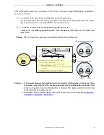
This document describes an operation overview of the sample program, as well as how to use the sample program and 

how to set and use the watchdog timer.  In the sample program, a reset signal generated by an overflow of the 

watchdog timer is generated at a 50% chance of occurrence during a switch input, by setting the runaway detection time 

to 131 ms.


CONTENTS 

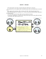
CHAPTER  1  OVERVIEW ...................................................................................3 

1.1  Main Contents of Initial Settings ..............................................................4 

1.2 Contents 

Following the Main Loop...........................................................4 

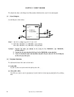
CHAPTER  2   CIRCUIT  DIAGRAM ....................................................................6 

2.1 Circuit 

Diagram ........................................................................................6 

2.2 Peripheral 

Hardware ................................................................................6 

CHAPTER  3   SOFTWARE .................................................................................7 

3.1 File 

Configuration.....................................................................................7 

3.2 Internal 

Peripheral 

Functions to Be Used ................................................8 

3.3  Initial Settings and Operation Overview...................................................8 
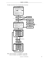
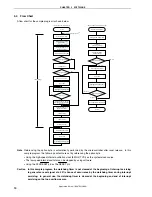
3.4 Flow 

Chart..............................................................................................10 

CHAPTER  4   SETTING  METHODS ................................................................11 

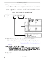
4.1  Watchdog Timer (WDT) Setting.............................................................11 

CHAPTER  5   OPERATION  CHECK  USING  THE  DEVICE ..........................19 

5.1  Building the Sample Program ................................................................19 

5.2 Operation 

with the Device......................................................................21 

CHAPTER  6   RELATED  DOCUMENTS..........................................................23 

APPENDIX  A   PROGRAM  LIST......................................................................24 

APPENDIX  B   REVISION  HISTORY ...............................................................36 


Target devices


78K0S/KA1+ microcontroller


78K0S/KB1+ microcontroller


78K0S/KU1+ microcontroller


78K0S/KY1+ microcontroller


Document No.    U18847EJ1V0AN00 (1st edition) 
Date Published   October  2007 N 


Printed in Japan 

   2007 


Summary of Contents for 78GK0S/K 1+ Series

Page 1: ...ing the Main Loop 4 CHAPTER 2 CIRCUIT DIAGRAM 6 2 1 Circuit Diagram 6 2 2 Peripheral Hardware 6 CHAPTER 3 SOFTWARE 7 3 1 File Configuration 7 3 2 Internal Peripheral Functions to Be Used 8 3 3 Initial Settings and Operation Overview 8 3 4 Flow Chart 10 CHAPTER 4 SETTING METHODS 11 4 1 Watchdog Timer WDT Setting 11 CHAPTER 5 OPERATION CHECK USING THE DEVICE 19 5 1 Building the Sample Program 19 5 2...

Page 2: ...y To minimize risks of damage to property or injury including death to persons arising from defects in NEC Electronics products customers must incorporate sufficient safety measures in their design such as redundancy fire containment and anti failure features NEC Electronics products are classified into the following three quality grades Standard Special and Specific The Specific quality grade app...

Page 3: ...s about every 120 ms SW On turned on for at least 10 ms Input LED2 LED1 Output Blinks about every 120 ms Lights LED2 LED1 Output Blinks about every 60 ms 1 2 During interrupt servicing execution After WDT reset generation Main processing Interrupt servicing WDT clear WDT clear WDT clear WDT clear WDT clear WDT clear About 120 ms X ms About 10 ms Chattering removal About 60 ms About 60 ms Switch on...

Page 4: ...he valid edge of INTP1 external interrupt to the falling edge Enabling interrupt Note This is set by using the option byte 1 2 Contents Following the Main Loop After completion of the initial settings LED1 out of the two LEDs LED1 LED2 blinks about every 120 ms in the main loop LED2 LED1 Output Blinks about every 120 ms Interrupt servicing is performed by detecting the falling edge of the INTP1 pi...

Page 5: ...n processing Interrupt servicing WDT clear WDT clear WDT clear WDT clear WDT clear WDT clear About 120 ms X ms About 10 ms Chattering removal About 60 ms About 60 ms Switch on Switch off 1 X ms 10 ms 60 ms 131 ms No overflow occurs Interrupt servicing continues WDT overflow time 220 fX About 131 ms fX 8 MHz 2 X ms 10 ms 60 ms 131 ms An overflow occurs A WDT reset is generated during interrupt serv...

Page 6: ...icrocontrollers Cautions 1 Connect the AVREF pin directly to VDD only for the 78K0S KA1 and 78K0S KB1 microcontrollers 2 Connect the AVSS pin directly to GND only for the 78K0S KB1 microcontroller 3 Leave all unused pins open unconnected except for the pins shown in the circuit diagram and the AVREF and AVSS pins 2 2 Peripheral Hardware The peripheral hardware to be used is shown below 1 Switch SW...

Page 7: ...m Assembly language version main c C language version Source file for hardware initialization processing and main processing of microcontroller zNote zNote op asm Assembler source file for setting the option byte sets the system clock source z z wdt prw Work space file for integrated development environment PM z wdt prj Project file for integrated development environment PM z Note main asm is incl...

Page 8: ...e falling edge of the INTP1 pin was detected processing is identified as chattering and returned to the main loop If INTP1 is at low level switch is turned on after about 10 ms have elapsed since edge detection the following processing is advanced Either of the following operations is performed at a 50 chance of occurrence depending on the switch input timing 1 If an overflow is not caused by the ...

Page 9: ... Setting the valid edge of INTP1 external interrupt to the falling edge Enabling interrupt Setting VLVI to 2 85 V 0 15 V and starting low voltage detection operation Setting so that an internal reset signal is generated when VDD VLVI VDD VLVI Clearing the watchdog timer WDT reset LVI reset Lighting LED2 Reset other than by WDT Reset source check 2 POC reset or external reset Blinking LED1 every 12...

Page 10: ...ion Yes No Lighting LED2 Turning off LED1 and LED2 No Yes Clearing the watchdog timer 200 s wait 120 ms wait Clearing the watchdog timer Clearing the watchdog timer INTP1 pin input level Low level High level Clearing the INTP1 interrupt request μ Note Referencing the option byte is automatically performed by the microcontroller after reset release In this sample program the following contents are ...

Page 11: ...ration During Detection at Less than 2 7 V Application Note For how to set registers refer to the user s manual of each product 78K0S KU1 78K0S KY1 78K0S KA1 78K0S KB1 For assembler instructions refer to the 78K 0S Series Instructions User s Manual 4 1 Watchdog Timer WDT Setting The watchdog timer is controlled by the following two types of registers Watchdog timer mode register WDTM Watchdog time...

Page 12: ...dless of the written value Refer to 3 Setting the oscillation control of the low speed internal oscillator Cautions 1 Set bits 7 6 and 5 to 0 1 and 1 respectively 2 After reset is released WDTM can be written only once If writing is attempted a second time an internal reset signal is generated However if 1 and x are set for WDCS4 and WDCS3 respectively and the watchdog timer is stopped at the firs...

Page 13: ...e stopped Operation clock Only low speed internal oscillation clock operation clock cannot be selected Setting the oscillation of the low speed internal oscillator to Can be stopped by using software Operation clock The low speed internal oscillation clock system clock or watchdog timer operation stop can be selected Figure 4 3 Format of Option Byte Only Oscillation Control of Low Speed Internal O...

Page 14: ...ge Option byte address 0080H The option byte setting value is 1xx1xxx0 x don t care bits 7 and 4 must be set to 1 When the software is described together with the protect byte setting the following results In the example below bits 6 5 and 1 are set to 0 and bits 3 and 2 are set to 1 0 1 1 Operation clock selection 0 1 System clock fX Overflow time setting 1 1 1 2 20 fX 1 x x x 0 1 x x Oscillation...

Page 15: ... the low speed internal oscillation clock is selected regardless of the written value Option byte address 0080H The option byte setting value is 1xx1xxxx x don t care bits 7 and 4 must be set to 1 When the software is described together with the protect byte setting the following results In the example below bits 6 5 and 1 are set to 0 and bits 3 2 and 0 are set to 1 0 1 1 0Note 0Note 1 1 1 WDTM O...

Page 16: ...ting value is 1xx1xxx0 x don t care bits 7 and 4 must be set to 1 When the software is described together with the protect byte setting the following results In the example below bits 6 5 and 1 are set to 0 and bits 3 and 2 are set to 1 0 1 1 Operation clock selection 1 Overflow time setting x x x Invalid setting due to watchdog timer operation stop x Watchdog timer operation stop 1 x x x 0 1 x x ...

Page 17: ...t value WAIT_200US DEC A BNZ WAIT_200US 0 5 us clk 10 clk 40 count 200 us WAIT_LVI MOV WDTE 0ACH Clear the watchdog timer BT LVIF WAIT_LVI Branch if VDD VLVI SET1 LVIMD Set so that an internal reset signal is generated when VDD VLVI MAIN_LOOP XOR P2 00000001B Reverse output of LED1 MOV CNT120 120 Assign the 120 ms wait count value WAIT_120MS CALL WAIT_1MS Subroutine call for a 1 ms wait DBNZ CNT12...

Page 18: ...r ucCnt200us 0 ucCnt200us 9 ucCnt200us Wait of about 200 us NOP while LVIF Wait for VDD VLVI WDTE 0xAC Setting the WDT overflow time and operation clock Clear the watchdog timer LVIMD 1 Set so that an internal reset signal is generated when VDD VLVI void main void unsigned int unCnt120ms 16 bit variable for 120 ms wait EI Enable vector interrupt while 1 P2 0b00000001 Reverse output of LED1 for unC...

Page 19: ...clicking the icon For how to build other downloaded programs refer to CHAPTER 3 REGISTERING INTEGRATED DEVELOPMENT ENVIRONMENT PM PROJECTS AND EXECUTING BUILD in the 78K0S Kx1 Sample Program Startup Guide Application Note For the details of how to operate PM refer to the PM Project Manager User s Manual 1 Start PM 2 Select wdt prw by clicking Open Workspace from the File menu and click Open A work...

Page 20: ...e will be selected by default and click OK Select the device name Click the OK button 4 Click Build button When the source files are built normally the message I3500 Build completed normally will be displayed 5 Click the OK button in the message window A HEX file for flash memory writing will be created Click Click A HEX file for flash memory writing will be generated Go to 5 2 Application Note U1...

Page 21: ...ing prepared An example of how to connect the device and peripheral hardware switch and LEDs to be used is shown below 1 2 3 4 5 6 7 8 9 10 11 12 13 14 15 30 29 28 27 26 25 24 23 22 21 20 19 18 17 16 LED2 P20 P21 INTP1 SW VSS VDD VDD VDD RESET 78K0S KB1 microcontroller LED1 VDD VDD An operation example of the device to which this sample program has been written is described below 1 Operation befor...

Page 22: ...er After reset release LED2 lights and LED1 blinks about every 120 ms Remark LED2 is turned off by a reset signal generated by other than the watchdog timer SW On turned on for at least 10 ms Input LED2 LED1 Output Blinks about every 120 ms Lights LED2 LED1 Output Blinks about every 60 ms 1 2 During interrupt servicing execution After WDT reset generation Main processing Interrupt servicing WDT cl...

Page 23: ...iler User s Manual Operation PDF PM Project Manager User s Manual PDF SM System Simulator Operation User s Manual PDF 78K0S KA1 Simplified Flash Writing Manual MINICUBE2 Information PDF Sample Program Startup Guide PDF Sample Program Initial Settings LED Lighting Switch Control PDF Sample Program Interrupt External Interrupt Generated by Switch Input PDF 78K0S Kx1 Application Note Sample Program L...

Page 24: ... the watchdog timer is cleared about 70 ms after the interrupt of the SW input was generated Normally an overflow should be avoided by clearing the watchdog timer at the beginning and end of an interrupt Principal setting contents Set the low voltage detection voltage VLVI to 2 85 V 0 15 V Generate an internal reset signal low voltage detector when VDD VLVI after VDD VLVI Set the CPU clock frequen...

Page 25: ... P47 P120 P123 P130 All unused ports are set as the output mode Vector table XVCT CSEG AT 0000H DW RESET_START 00 RESET DW RESET_START 02 DW RESET_START 04 DW RESET_START 06 INTLVI DW RESET_START 08 INTP0 DW INTERRUPT_P1 0A INTP1 DW RESET_START 0C INTTMH1 DW RESET_START 0E INTTM000 DW RESET_START 10 INTTM010 DW RESET_START 12 INTAD DW RESET_START 14 DW RESET_START 16 INTP2 DW RESET_START 18 INTP3 ...

Page 26: ...t the clock 1 MOV PCC 00000000B The clock supplied to the CPU fcpu fxp fx 4 2 MHz MOV LSRCM 00000001B Stop the oscillation of the low speed internal oscillator Initialize the port 2 MOV P2 00000011B Set output latches of P20 P21 as high turn off LED1 LED2 and P22 P23 as low MOV PM2 11110000B Set P20 P23 as output mode Check the reset source MOV A RESF Read the reset source BF A 4 CHECK_LVI Go to C...

Page 27: ... Set P00 P03 as output mode Initialize the port 3 MOV P3 00000000B Set output latches of P30 P33 as low MOV PM3 11110000B Set P30 P33 as output mode Initialize the port 4 MOV P4 00000000B Set output latches of P40 P47 as low MOV PU4 00001000B Connect on chip pull up resistor to P43 MOV PM4 00001000B Set P43 as input mode P40 P42 and P44 P47 as output mode Initialize the port 12 MOV P12 00000000B S...

Page 28: ...ue 10 ms wait to handle chattering WAIT_10MS CALL WAIT_1MS Subroutine call for a 1 ms wait DBNZ CNT10 WAIT_10MS 1 ms x 10 count 10 ms CLR1 PIF1 Clear the INTP1 interrupt request Identification of chattering detection BT P4 3 END_INTP1 Branch if there is no switch input SW_ON Reverse LED1 XOR P2 00000001B Reverse output of LED1 MOV CNT60 60 Assign the 60 ms wait count value 60 ms wait WAIT_60MS CAL...

Page 29: ...e time in ms units that is indicated with num can be measured more accurately by setting as follows saddr short direct addressable memory area MOV saddr num loopxx CALL WAIT_1MS DBNZ saddr loopxx WAIT_1MS PUSH BC Save the BC register data to the stack MOV B 220 Assign the 220 time loop count value LOOP_220 NOP NOP NOP NOP NOP NOP DBNZ B LOOP_220 220 time loop for a 1 ms wait NOP NOP POP BC Restore...

Page 30: ...learing the watchdog timer at the beginning and end of an interrupt Principal setting contents Declare a function run by an interrupt INTP1 fn_intp1 Select fx as the watchdog timer WDT count clock and set the overflow time to 131 07 ms Set the low voltage detection voltage VLVI to 2 85 V 0 15 V Generate an internal reset signal low voltage detector when VDD VLVI after VDD VLVI Set the CPU clock fr...

Page 31: ...cribed at the C source level pragma NOP NOP instructions can be described at the C source level pragma interrupt INTP1 fn_intp1 Interrupt function declaration INTP1 Initialization after RESET sreg unsigned char ucRESF 8 bit variable for reset source check high speed internal RAM area void hdwinit void unsigned char ucCnt200us 8 bit variable for 200 us wait Detect low voltage initialize the watchdo...

Page 32: ... 0 15 V LVION 1 Enable the low voltage detector operation for ucCnt200us 0 ucCnt200us 9 ucCnt200us Wait of about 200 us NOP while LVIF Wait for VDD VLVI WDTE 0xAC Clear the watchdog timer LVIMD 1 Set so that an internal reset signal is generated when VDD VLVI Set the clock 2 PPCC 0b00000001 The clock supplied to the peripheral hardware fxp fx 2 4 MHz The clock supplied to the CPU fcpu fxp 4 MHz In...

Page 33: ...nterrupt INTM0 0b00000000 Set the valid edge of INTP1 to falling edge PIF1 0 Clear invalid interrupt requests in advance PMK1 0 Release the INTP1 interrupt mask return Main loop void main void unsigned int unCnt120ms 16 bit variable for 120 ms wait EI Enable vector interrupt while 1 P2 0b00000001 Reverse output of LED1 for unCnt120ms 0 unCnt120ms 6666 unCnt120ms Wait of about 120 ms NOP WDTE 0xAC ...

Page 34: ... for chattering removal NOP PIF1 0 Clear the INTP1 interrupt request while P4 3 Processing during SW input P2 0b00000001 Reverse output of LED1 for unCnt 0 unCnt 3333 unCnt Wait of about 60 ms NOP WDTE 0xAC Clear the watchdog timer return Application Note U18847EJ1V0AN 34 ...

Page 35: ...00B Option byte area Low speed internal oscillator can be stopped by software High speed internal oscillation clock 8 MHz is selected for system clock source P34 RESET pin is used as RESET pin DB 11111111B Protect byte area for the self programming mode All blocks can be written or erased end Application Note U18847EJ1V0AN 35 ...

Page 36: ...APPENDIX B REVISION HISTORY Edition Date Published Page Revision 1st edition October 2007 Application Note U18847EJ1V0AN 36 ...

Page 37: ...l 02 8175 9600 http www tw necel com NEC Electronics Singapore Pte Ltd 238A Thomson Road 12 08 Novena Square Singapore 307684 Tel 6253 8311 http www sg necel com NEC Electronics Korea Ltd 11F Samik Lavied or Bldg 720 2 Yeoksam Dong Kangnam Ku Seoul 135 080 Korea Tel 02 558 3737 http www kr necel com For further information please contact G0706 Europe NEC Electronics Europe GmbH Arcadiastrasse 10 4...

Reviews: