Motorola CompactPCI CPN5365, Installation And Use Manual
The Motorola CompactPCI CPN5365 is a cutting-edge technology offering outstanding performance. Ensure smooth installation and optimal usage by referring to our comprehensive "Installation And Use Manual." Download this manual for free from our website and unlock the full potential of your Motorola CompactPCI CPN5365.
Share
Download


Reviews:
No comments
Related manuals for CompactPCI CPN5365
A
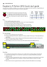
Brand: Raspberry Pi Pages: 2
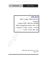
EPIC-HD07
Brand: Aaeon Pages: 97
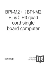
BPI-M2+
Brand: Banana Pi Pages: 88
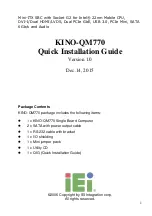
KINO-QM770
Brand: IEI Technology Pages: 15
HPCIE-Q470
Brand: IEI Technology Pages: 16
ICE-BDE-T7
Brand: IEI Technology Pages: 98
WAFER-JL-N5105
Brand: IEI Technology Pages: 79
TX 4000C
Brand: NMS Communications Pages: 58
iW-RainboW-G25M
Brand: iWave Pages: 52

NANO-LX-800
Brand: IEI Technology Pages: 8
PSC-586VGA
Brand: IEI Technology Pages: 31
efus A9X
Brand: F&S Pages: 36
PC/104 Single Board Computer with STPC Atlas CPU, and VGA, LCD, LAN, SSD, on-board RAM, 4xCOM,...
Brand: Lanner electronics Pages: 44
A10-OLINUXINO-LIME-4GB
Brand: OLIMEX Pages: 46
PME 68-1B
Brand: Radstone Pages: 132
PPM-LX800-G
Brand: WinSystems Pages: 56
VT-SBC-3399
Brand: Vantron Pages: 44

HS-4010
Brand: Boser Pages: 45


