background image

CC-Link Embedded I/O Adapter
User's Manual

Summary of Contents for CC-Link

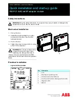
Page 1: ...CC Link Embedded I O Adapter User s Manual ...

Page 2: ......

Page 3: ...en required and always forward it to the end user Design Precautions DANGER When there are communication errors with the data link the communication error station will enter the following condition Build an interlock circuit into the sequence program to operate system safely by using the communication state information An accident may occur by a false output or a malfunction 1 Turn off all input f...

Page 4: ... embedded I O adapter check the rated voltage and terminal layout and make sure the wiring is done correctly Connecting a power supply that differs from the rated voltage or wiring it incorrectly may cause fire failure or malfunction Make sure that there are no foreign substances such as sawdust or wiring debris inside the CC Link embedded I O adapter Such debris could cause fire failure or malfun...

Page 5: ...y the CC Link embedded I O adapter Doing so could cause failure malfunction injury or fire Because the case of the CC Link embedded I O adapter is made of resin be careful not to drop it or expose it to strong impact It may damage the CC Link embedded I O adapter Before mounting or dismounting the user board loaded with the CC Link embedded I O adapter to or from an enclosure always switch power o...

Page 6: ...ion 4 2 1 4 3 1 5 1 5 2 Mar 2006 SH NA 080324E C Correction Chapter 3 Section 5 1 Sep 2006 SH NA 080324E D Addition Section 6 2 2 Correction Section 6 2 1 Japanese Manual Version SH 080323 D This manual confers no industrial property rights or any rights of any other kind nor does it confer any patent licenses Mitsubishi Electric Corporation cannot be held responsible for any problems involving in...

Page 7: ...dapters 4 1 4 1 1 AJ65MBTL1N 16D CC Link embedded input adapter 4 1 4 1 2 AJ65MBTL1N 32D CC Link embedded input adapter 4 3 4 2 Specifications for Output Adapters 4 5 4 2 1 AJ65MBTL1N 16T CC Link embedded output adapter 4 5 4 2 2 AJ65MBTL1N 32T CC Link embedded output adapter 4 7 4 3 Specifications for Combined Adapters 4 9 4 3 1 AJ65MBTL1N 16DT CC Link embedded combined adapter 4 9 5 HANDLING CC ...

Page 8: ... A1SJ61BT11 Sold separately IB 66721 13J872 CC Link System Master Local Module type AJ61QBT11 A1SJ61QBT11 User s Manual This manual describes the system configuration performance specification function handling wiring and troubleshooting for AJ61QBT11 and A1SJ61QBT11 Sold separately IB 66722 13J873 Conformation to the EMC Directive and Low Voltage Instruction For details on making Mitsubishi PLC c...

Page 9: ...user board 3 Flexible noise reduction measures Depending on external noise environment the user board can be equipped with a noise filter to enhance noise resistance as necessary 4 Insulation method The adapter power supply uses a transformer insulation method and the external I O uses a photocoupler insulation method 5 Overload protection function overvoltage protection function and overheat prot...

Page 10: ... the Compact CC Link Embedded I O Adapter Type The following shows how to identify the type of a CC Link embedded I O adapter AJ65MBTL1N 16DT D T DT 16 16 points 24VDC input Transistor output 24VDC input transistor output complex 32 32 points 1 ...

Page 11: ...onverter as the load for a CC Link embedded transistor output adapter having a maximum load current of 0 1A a rush current flows when the adapter is turned on and at fixed intervals during operation For this reason malfunctions may occur if the average current is set When the above load is used connect resistance or inductance in parallel to the load or use an output adapter having a large maximum...

Page 12: ...k input 8 points transistor output 0 1A sink output Section 4 3 1 1 5 About the Generic Abbreviated and Technical Terms Used in This Manual The abbreviated and technical terms used in this manual are listed below Generic abbreviated technical term Description CC Link Abbreviation of Control Communications Link Master local module Generic term for the QJ61BT11 AJ61BT11 A1SJ61BT11 AJ61QBT11 and A1SJ...

Page 13: ...1 5 1 5 MELSEC A 1 OVERVIEW MEMO ...

Page 14: ... embedded I O adapter normally Turns on when normal data is received from master station and turns off when time has expired L ERR On Communication data error Flicker at regular intervals Indicates that the station number setting or transmission speed setting switch position was changed while power is on Flicker at irregular intervals Indicates that the terminal resistor is left unconnected or tha...

Page 15: ...ge of 1 to 64 1 Duplicate station number cannot be set Ten s place One s place Station number 40 20 10 8 4 2 1 1 OFF OFF OFF OFF OFF OFF ON 2 OFF OFF OFF OFF OFF ON OFF 3 OFF OFF OFF OFF OFF ON 4 OFF OFF OFF OFF OFF OFF OFF 10 OFF OFF ON OFF OFF OFF OFF 11 OFF OFF ON OFF OFF OFF ON 64 ON ON OFF OFF ON OFF OFF Example Set the switches as below when setting the station number to 32 Ten s place One s...

Page 16: ...ns Operating environment No corrosive gas present Operating height 2000 m 6562 ft or less 3 Installation area On the control board Over voltage category 1 II or less Pollution rate 2 2 or less 1 Indicates the location where the device is connected from the public cable network to the device structure wiring area Category II applies to the devices to which the power is supplied from a fixed equipme...

Page 17: ...3 2 3 2 MELSEC A 3 SPECIFICATIONS MEMO 3 ...

Page 18: ... 1 7mA or lower Input resistance Approx 5 1kΩ Response OFF ON 1 5ms or lower at 24V DC time ON OFF 1 5ms or lower at 24V DC Input type Positive common sink Wiring method for common 16 points 1 common CC Link station type Remote I O station Number of occupied stations 1 station 32 points assignment use 16 points I O adapter Voltage 20 4 to 26 4V DC ripple rate within 5 power supply Current 35mA or ...

Page 19: ... B19 A19 B18 A18 B17 A17 B16 A16 B15 A15 B14 A14 B13 A13 B12 A12 B11 A11 B10 A10 B09 A09 B08 A08 B07 A07 B06 A06 B05 A05 B04 A04 B03 22000pF 630V A03 B02 A02 B01 A01 DA AJ65MBTL1N 16D 2 Adapter power supply 1 Insulation DA DB DG SLD Circuit board IC DB DG FG To G A To G A To G A OE OUT OE IN SD OUT SD IN RD RDGON GND X0 X1 X2 X3 X4 X5 X6 R R X7 X8 X9 XA XB XC XD XE XF COM COM 24V DC DC 24V 24V 24G...

Page 20: ...kΩ Response OFF ON 1 5ms or lower at 24V DC time ON OFF 1 5ms or lower at 24V DC Input type Positive common sink Wiring method for common 32 points 1 common CC Link station type Remote I O station Number of occupied stations 1 station 32 points assignment use 32 points I O adapter Voltage 20 4 to 26 4V DC ripple rate within 5 power supply Current 45mA or lower at 24V DC Noise durability DC type no...

Page 21: ... A07 B06 A06 B05 A05 B04 A04 B03 A03 B02 A02 X13 X14 X15 X16 R X17 X18 X19 X1A X1B X1C X1D X1E X1F COM COM 24V 24V X13 X14 X15 X16 X17 X18 X19 X1A X1B X1C X1D X1E X1F 24V DC COM R Insulation DC DC A15 B14 X11 X12 X11 X12 A17 B16 A16 B15 B31 A31 B30 A30 B29 A29 B28 A28 B27 A27 B26 A26 B25 A25 B24 A24 B23 A23 B22 DA AJ65MBTL1N 32D 2 DA DB DG SLD Circuit board IC DB DG FG To G A To G A To G A OE OUT ...

Page 22: ...N OFF 1ms or lower rated load resistive load External Voltage 10 2 to 26 4V DC ripple ratio within 5 Power supply for output Current 10mA or lower When all points are ON at 24V DC Not including external load current Surge suppression Zener diode Wiring method for common 16 points 1 common CC Link station type Remote I O station Number of occupied stations 1 station 32 points assignment use 16 poin...

Page 23: ...A18 B17 A17 B16 A16 B15 A15 B14 A14 B13 A13 B12 A12 B11 A11 B10 A10 B09 A09 B08 A08 B07 A07 B06 A06 B05 A05 B04 A04 B03 22000pF 630V A03 B02 A02 B01 A01 DA 2 1 DA DB DG SLD DB DG FG OE OUT OE IN SD OUT SD IN RD RDGON GND Y0 Y1 Y2 Y3 Y4 Y5 Y6 Y7 Y8 Y9 YA YB YC YD YE YF CTL CTL COM COM 24V DC DC 24V 24V 24G FG 24G 24G Y0 L Y1 Y2 Y3 Y4 Y5 Y6 Y7 Y8 Y9 YA YB YC YD YE YF 12 24V DC CTL COM L Link IC Adap...

Page 24: ...ated load resistive load External Voltage 10 2 to 26 4V DC ripple ratio within 5 Power supply for output Current 15mA or lower When all points are ON at 24V DC Not including external load current Surge suppression Zener diode Wiring method for common 32 points 1 common CC Link station type Remote I O station Number of occupied stations 1 station 32 points assignment use 32 points I O adapter Volta...

Page 25: ... B04 A04 B03 A03 B02 A02 Insulation Y13 Y14 Y15 Y16 Y17 Y18 Y19 Y1A Y1B Y1C Y1D Y1E Y1F CTL CTL DC DC Y13 Y14 Y15 Y16 Y17 Y18 Y19 Y1A Y1B Y1C Y1D Y1E Y1F CTL COM A15 B14 Y11 Y12 Y11 Y12 A17 B16 A16 B15 B31 A31 B30 A30 B29 A29 B28 A28 B27 A27 B26 A26 B25 A25 B24 A24 B23 A23 B22 DA AJ65MBTL1N 32T 2 DA DB DG SLD Circuit board IC DB DG FG To G A To G A To G A OE OUT OE IN SD OUT SD IN RD RDGON GND Y0 ...

Page 26: ...prox 3 3k Ω Protection functions Overload over voltage and overheat protection OFF ON 1 5ms or lower at 24V DC OFF ON 1ms or lower Response time ON OFF 1 5ms or lower at 24V DC Response time ON OFF 1ms or lower rated load resistive load External Voltage 19 2 to 26 4V DC ripple ratio within 5 Power supply for output Current 5mA or lower When all points are ON at 24V DC Not including external load c...

Page 27: ...18 A18 B17 A17 B16 A16 B15 A15 B14 A14 B13 A13 B12 A12 B11 A11 B10 A10 B09 A09 B08 A08 B07 A07 B06 A06 B05 A05 B04 A04 B03 22000pF 630V A03 B02 A02 B01 A01 DA AJ65MBTL1N 16DT 2 1 DA DB DG SLD DB DG FG OE OUT OE IN SD OUT SD IN RD RDGON GND X0 X1 X2 X3 X4 X5 X6 R R X7 Y8 Y9 YA YB YC YD YE YF 24V DC 24V DC 24G DC 24G DC 24V DC DC 24V 24V 24G FG 24G 24G X0 X1 X2 X3 X4 X5 X6 X7 Y8 Y9 YA YB YC YD YE YF...

Page 28: ...mbedded I O adapter Because the case of the CC Link embedded I O adapter is made of resin be careful not to drop it or expose it to strong impact It may damage the CC link embedded I O adapter When disposing of this product treat it as industrial waste Use the CC Link embedded I O adapter in an environment that meets the general specifications contained in this manual Using this adapter in an envi...

Page 29: ...susceptible to noise keep them as far away as possible from the other patterns power supply I O signal that include noise 6 When the adapters are not cascaded always connect GND and RDGON 16 point adapter A17 pin and A18 pin 32 point adapter A26 pin and A27 pin on the board side 7 Wire the FG pattern so that it does not cross the I O patterns on the front and back sides of the board Doing so makes...

Page 30: ... not store the CC Link embedded I O adapter in dusty gas corrosive or similar environment that may deteriorate the solderability of the adapter pins b Do not touch the pins of the CC Link embedded I O adapter directly Doing so can cause the deterioration of solderability c Do not bend or cut the pins of the CC Link embedded I O adapter In addition do not use the CC Link embedded I O adapter that h...

Page 31: ...adapters internal elements but not for external devices Overload protection function 1 The overload protection function is activated in a load condition of 1 A to 3 A per point 2 The overload protection function automatically returns to normal operation when the load drops to the rated value Overvoltage protection function 1 This function protects elements from an abrupt surge caused when a coil l...

Page 32: ...the pin numbers when 32 point CC Link embedded I O adapters are used OE IN OE IN SD IN RD OE OUT SD OUT SD IN RD OPEN A20 A19 B18 A20 A19 A18 RDGON GND A17 B18 B19 A21 A22 B21 B22 DA DB DG FG OE OUT SD OUT DA DA DB DG SLD FG DB DG FG B20 B19 A21 A22 B21 B22 B20 A18 A17 RDGON GND CC Link enbedded I O adapter 1 CC Link enbedded I O adapter 2 POINT Since the cascade communication pattern is easily af...

Page 33: ...re from each other Not doing so could result in noise that would cause malfunction Always ground the FG terminal to the protective ground conductor Doing so may cause electric shock or malfunction Securely solder the CC link embedded I O adapter to install it to a user board Defective contact could cause malfunction Make sure that the communication cable connected to the adapter is kept in the duc...

Page 34: ...ct the terminal resistor to the compact remote I O adapter terminating station in the locations shown below The terminal resistor is provided with the master module DA DB DG SLD FG Terminal resistor 2 Use the CC Link dedicated cables in the CC Link system If the cables other than the CC Link dedicated cables are used we cannot guarantee the performance of the CC Link system Refer to the CC Link Pa...

Page 35: ...ights are off in many cases Exchange the CC Link embedded I O adapter PW L RUN L ERR PW L RUN L ERR PW L RUN L ERR The L RUN lights on the CC Link embedded I O adapter B and beyond are off indicating the transmission cable between the CC Link embedded I O adapter A and B has been disconnected or removed from the terminal block Identify the disconnected point by referring to the LED status and corr...

Page 36: ...indicating the setting switch for CC Link embedded I O adapter A is set out of range transmission speed 5 to 9 station number 65 or greater Correct the setting switch of the CC Link embedded I O adapter and restart the power supply PW L RUN L ERR PW L RUN L ERR PW L RUN L ERR The L ERR of the CC Link embedded I O adapter B is lit indicating that CC Link embedded I O adapter B is being affected by ...

Page 37: ...ation via the LED display switch Leakage current CC Link embedded Input adapter DC input sink Connect a resistor so that the voltage between the input terminal and COM1 becomes lower than the OFF voltage Resistor CC Link embedded Input adapter DC input sink A calculation example used to obtain the resistance value to be connected is shown on the following page Example 2 Input signals do not turn o...

Page 38: ...put impedance 5 1 k 4 7 k 24 V DC Current I Calculation of resistor R value Current I should be as follows so that the terminal voltage of the AJ65MBTL1N 16D is 6 V or less 24 6 V 4 7 k 3 83 mA Therefore connect a resistor R that will give a current I of 3 83 mA or more Resistor R to be connected is as follows 6 V R 3 83 6 V 5 1 k 6 V R 3 83 1 18 mA 6 V 2 65 mA R 2 26 k R Assuming that resistor R ...

Page 39: ... stage of transister Tr1 gate and Y0 utput turns on by 100 s SW External power supply 24V at On Output Y0 Approx 100 s 10ms or less When the external power turns ON OFF check that the external power supply rising edge must be 10ms or more and switch the SW1 to the primary side of external power supply Primary side Secondary side SW1 external power supply PLC When switching to the secondary side of...

Page 40: ...xternal Dimensions Appendix 1 1 AJ65MBTL1N 16 3 5 31 5 53 2 09 3 5 22 1 24 0 14 0 87 0 14 Unit mm inch Recommended board dimension drawing top view 5 5 0 22 5 5 0 22 0 95 0 04 A22 B01 A01 7 5 B22 2 0 08 0 05 42 1 65 0 1 0 30 2 0 08 0 05 Unit mm inch APP ...

Page 41: ...pendix 1 2 AJ65MBTL1N 32 3 5 85 22 31 5 3 5 0 87 3 35 0 14 1 24 0 14 Unit mm inch Recommended board dimension drawing top view 60 2 36 0 1 B01 A01 19 5 7 5 2 0 08 5 5 0 22 0 95 0 04 A31 B31 2 0 08 0 05 0 77 0 30 0 05 Unit mm inch APP ...

Page 42: ... by the user 2 Onerous repair term after discontinuation of production 1 Mitsubishi shall accept onerous product repairs for seven 7 years after production of the product is discontinued Discontinuation of production shall be notified with Mitsubishi Technical Bulletins etc 2 Product supply including repair parts is not available after production is discontinued 3 Overseas service Overseas repairs...

Page 43: ......

Page 44: ... without notice When exported from Japan this manual does not require application to the Ministry of Economy Trade and Industry for service transaction permission HEAD OFFICE TOKYO BUILDING 2 7 3 MARUNOUCHI CHIYODA KU TOKYO 100 8310 JAPAN NAGOYA WORKS 1 14 YADA MINAMI 5 CHOME HIGASHI KU NAGOYA JAPAN ...

Reviews: