background image

Date: February, 2006 / Issue 1.0

Service Manual

Model : U8500

Service Manual

U8500

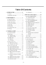
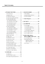
Summary of Contents for U8500

Page 1: ...Date February 2006 Issue 1 0 Service Manual Model U8500 Service Manual U8500 ...

Page 2: ...RF filter FL1001 34 3 5 9 VCTCXO X1000 35 3 5 10 Bluetooth 35 3 BB Technical Description 37 3 6 Baseband DBB MSM6250 37 3 6 1 General Description 37 3 7 Hardware Architecture 38 3 7 1 Block Diagram MSM6250 39 3 8 Subsystem MSM6250 40 3 8 1 ARM Microprocessor Subsystem 40 3 8 2 UMTS Subsystem 40 3 8 3 GSM Subsystem 40 3 8 4 RF Interface 40 3 8 5 Serial Bus Interface SBI 40 3 8 6 Wideband CODEC 41 3...

Page 3: ...103 4 13 Main LCD Trouble 104 4 14 Keypad Backlight Trouble 106 4 15 Folder ON OFF Trouble 107 4 16 Camera Direction Detection Trouble 108 4 17 Trans Flash Trouble 109 4 18 Audio Trouble Shooting 110 4 19 Charger Trouble Shooting 120 5 DOWNLOAD 123 5 1 Introduction 123 5 2 Downloading Procedure 123 5 3 Troubleshooting Download Errors 136 6 BLOCK DIAGRAM 141 6 1 BLK diagram 141 6 2 GSM WCDMA RF Blo...

Page 4: ...ible for any charges that result from such unauthorized use B Incidence of Harm If a telephone company determines that the equipment provided to customer is faulty and possibly causing harm or interruption in service to the telephone network it should disconnect telephone service until repair can be done A telephone company may temporarily disconnect service as long as repair is not done C Changes...

Page 5: ...ipment etc Interference from unsuppressed engines or electric motors may cause problems H Electrostatic Sensitive Devices ATTENTION Boards which contain Electrostatic Sensitive Device ESD are indicated by the sign Following information is ESD handling Service personnel should ground themselves by using a wrist strap when exchange system boards When repairs are made to a system board they should sp...

Page 6: ...800mAh Over 160 min GSM Tx Max Voice Standby Time Over 200 Hrs WCDMA DRX 1 28 with 800mAh Over 220 Hrs GSM Paging period 9 Antenna Internal type LCD Main 176 X 220 pixel TFT sub 96 X 96 pixel TFT LCD Backlight White LED Back Light 2way main sub common Camera 1 3 Mega pixel CMOS Vibrator Yes Cylinder Type LED Indicator No C MIC Yes Receiver Yes Earphone Jack Yes 12 pin Connectivity Bluetooth USB Vo...

Page 7: ...rage Temp 20 70 C Humidity 85 Max Reference Spec Min Typ Max Unit TA Power Available power 100 220 240 Vac No Item GSM DCS PCS 100k 1GHz 39dBm 9k 1GHz 39dBm MS allocated 1G A MHz 33dBm Channel 1G 12 75GHz 33dBm A M B MHz 39dBm Conducted B M 12 75GHz 33dBm 1 Spurious 100k 880MHz 60dBm 100k 880MHz 60dBm Emission 880M 915MHz 62dBm 880M 915MHz 62dBm Idle Mode 915M 1GHz 60dBm 915M 1GHz 60dBm 1G A MHz 5...

Page 8: ...r 0 1ppm 0 1ppm 4 Phase Error 5 RMS 5 RMS 20 PEAK 20 PEAK 3dB below reference sensitivity 3dB below reference sensitivity Frequency Error RA250 200Hz RA250 250Hz 5 Under Multipath and HT100 100Hz HT100 250Hz Interference Condition TU50 100Hz TU50 150Hz TU3 150Hz TU1 5 200Hz 0 100kHz 0 5dB 0 100kHz 0 5dB 200kHz 30dB 200kHz 30dB 250kHz 33dB 250kHz 33dB Due to 400kHz 60dB 400kHz 60dB Output RF modula...

Page 9: ...al Power control Power Tolerance Power control Power Tolerance Level dBm dB Level dBm dB 5 33 3 0 30 3 6 31 3 1 28 3 7 29 3 2 26 3 8 27 3 3 24 3 9 25 3 4 22 3 10 23 3 5 20 3 8 Transmitter Output Power 11 21 3 6 18 3 12 19 3 7 16 3 13 17 3 8 14 3 14 15 3 9 12 4 15 13 3 10 10 4 16 11 5 11 8 4 17 9 5 12 6 4 18 7 5 13 4 4 19 5 5 14 2 5 15 0 5 9 Burst timing Mask IN Mask IN ...

Page 10: ...tput Power 50dBm 3 84MHz Qin Qout PCCH quality levels 6 Out of synchronization handling of output power Toff DPCCH Ior 22 28dB Ton DPCCH Ior 24 18dB 7 Transmit OFF Power 56dBm 3 84MHz 8 Transmit ON OFF Time Mask 25us PRACH CPCH uplinlk compressed mode 25us 9 Change of TFC Power varies according to the data rate DTX DPCH off minimize interference between UE 10 Power setting in uplink compressed 3dB...

Page 11: ...MHz Interferer 40dBc 16 Error Vector Magnitude EVM 17 5 20dBm 12 2K 1DPDCH 1DPCCH 17 Transmit OFF Power 15dB SF 4 768Kbps Multi code transmission No Item GSM DCS PCS 1 Sensitivity TCH FS Class II 105dBm 105dBm 2 Co Channel Rejection C Ic 7dB Storage 30 85 TCH FS Class II RBER TU high FH 3 Adjacent Channel 200kHz C Ia1 12dB C Ia1 12dB Rejection 400kHz C Ia2 44dB C Ia2 44dB Wanted Signal 98dBm Wante...

Page 12: ... UE 20dBm output power Class3 44dBm 3 84MHz f 2050 2095 and 2185 2230MHz UE 20dBm output power Class3 30dBm 3 84MHz f 2025 2050 and 5 Out band Blocking 2230 2255MHz UE 20dBm output power Class3 15dBm 3 84MHz f 1 2025 and 2255 12500MHz UE 20dBm output power Class3 6 Spurious Response 44dBm CW UE 20dBm output power Class3 46dBm CW 10MHz 7 Intermodulation Characteristic 46dBm 3 84MHz 20MHz UE 20dBm o...

Page 13: ...Bm Under 3 6 mA Under 300 mA Paging 9period Tx Max GSM Under 5 3 mA Bluetooth Connected Paging 9period Level Change WCDMA GSM BAR 4 3 87 2 dBm 91 2 dBm BAR 3 2 97 2 dBm 96 2 dBm BAR 2 1 107 2 dBm 101 2 dBm BAR 1 0 111 2 dBm 106 2 dBm Indication Standby Bar 4 Over 3 82 0 03V Bar 4 3 3 81 0 03V Bar 3 2 3 74 0 03V Bar 2 1 3 67 0 03V Bar 1 Empty 3 50 0 03V Low Voltage 3 38 0 03V Stand by 3 50 0 03V Ta...

Page 14: ...nder 47 dBPA Max Under 36 dBPA 9 Sending Loudness Rating SLR 8 3dB 10 Receiving Loudness Rating RLR Nor 1 3 dB Max 12 3 dB 11 Side Tone Masking Rating STMR Min 25 dB 12 Echo Loss EL Min 40 dB 13 Sending Distortion SD Refer to Table 30 3 14 Receiving Distortion RD Refer to Table 30 4 15 Idle Noise Sending INS Max 55 dBm0p 16 Idle Noise Receiving INR Nor Under 45 dBPA Max Under 40 dBPA TDMA Noise GS...

Page 15: ...oltage Maximum Charging Voltage 4 2 V Maximum Charging Current 600 mA Normal Battery Capacity 800 mAh Charging Time Max 3 5 hours except for trickle charging time Full charging indication current charging icon stop current 60 mA Cut off voltage 3 28 V 2 PERFORMANCE 16 ...

Page 16: ... to eliminate intermediate frequencies directly converting signals between RF and baseband The EGSM DCS1800 and PCS1900 transmitters use a baseband to IF upconversion followed by an offset phase locked loop that translates the GMSK modulated signal to RF 1 QUALCOMM s branded chipset that implements a Zero IF radio architecture 3 TECHNICAL BRIEF U8500 high level RF functional block diagram ...

Page 17: ...thin the RTR6250 IC PLL and distribution functions with exception of the off chip loop filter The RTR analog baseband outputs are routed to the MSM6250 IC for further processing an interface shared with the RFR UMTS receive paths The UMTS transmit path begins with analog baseband signals from the MSM device that drive the RTR6250 IC Integrated PLL and VCO circuits generate the Tx LO used in the qu...

Page 18: ...taining the handset supply voltages using low dropout programmable regulators The device s general housekeeping functions include an ADC and analog multiplexer circuit for monitoring on chip voltage sources charging status and current flow as well as user defined off chip variables such as temperature RF output power and battery ID Various oscillator clock and counter circuits support IC and highe...

Page 19: ...e used to separate Rx and Tx signals in place of frequency duplexers this is accomplished in the switch module The EGSM DCS and PCS receive signals are routed to the RTR6250 through band selection filters and matching networks that transform single ended 50 Ωsources to differential impedances optimized for gain and noise figure Similar to the RFR the RTR input uses a differential configuration to ...

Page 20: ...3 TECHNICAL BRIEF 21 ...

Page 21: ...downconversion mixer are formed as follows 1 The dual Tx VCO output operating in the desired RF output frequency range is buffered within the RTR6250 IC then applied to the mixer RF port 2 The LO Generation and Distribution circuits that deliver the transmit path s LO for the baseband to IF upconversion also provides the offset LO signal that is applied to the feedback path s mixer LO port The mix...

Page 22: ...r given the VCO output level the subsequent passive devices losses and the control set point The maximum and minimum transmitter output power levels depend upon the operating band class and mobile station class per the applicable standard Transmitter timing requirements and inband and out of band emissions all dominated by the PA are also specified by the applicable standard The active dual Tx VCO...

Page 23: ...0 IC includes LO generation and distribution circuitry to reduce offchip component requirements The GPS RX LO source is created using the PLL control elements of the RTR6250 PLL2 via a discrete loop filter components in tandem with the VCO in the RFR6250 Using only this PLL signal the RFR6250 LO generation and distribution circuits create the necessary LO signals for the UMTS quadrature down conve...

Page 24: ... filtered and applied to the PA The PA device used in U8500 is Load Insensitive PA no need to use isolator and routed to the duplexer Tx port directly Transmit power is delivered from the duplexer to the antenna through the switch module The RTR6250 IC integrates LO generation and distribution circuits on chip substantially reducing off chip requirements Various modes and programmable features res...

Page 25: ... UHF_VCO_EN enables the VCO The RFR6250 IC accommodates single ended or differential LO inputs if singleended either pin can be active AC couple the inactive pin to ground using an appropriately valued capacitor 12 pF is used in U8500 The 27 pF capacitor should be used to AC couple the active pin to the VCO signal Using only the selected VCO signal the RFR6250 IC LO generation and distribution cir...

Page 26: ... error signal at the output of the charge pump This error signal is filtered by the loop filter and applied to the VCO tuning the output frequency such that the error is decreased Ultimately the loop forces the error to approach zero and the PLL is phase and frequency locked Many key PLL performance characteristics are largely determined by the loop filter design stability transitory response sett...

Page 27: ... frequency duplexer is not required The module includes lowpass filters for the GSM bands transmit paths to reduce out of band emissions PA harmonics in particular The GSM mode RF filters are located before their LNAs so their insertion losses are extremely critical 1 5 dB typical Other important parameters are Out of band rejection or attenuation levels Far out of band signals ranging from DC up ...

Page 28: ...d isolation depends on the PA channel power and Tx band losses between the PA and LNA Typical duplexer Tx band isolation value is 50 dB Passband ripple the loss of this fairly narrowband device is not flat across its passband Passband ripple increases the receive or transmit insertion loss at specific frequencies creating performance variations across the band s channels and should be controlled R...

Page 29: ...positive voltage DC supply operation while maintaining high efficiency and good linearity Primary bias to the SKY77410 is supplied directly from a three cell Ni Cd a singlecell Li Ion or other suitable battery with an output in the 3 2 to 4 2 volt range Power down is accomplished by setting the voltage on the low current reference pin to zero volts No external supply side switch is needed as typic...

Page 30: ... the transmitter characteristic over the channel variation and temperature Its detector coupling range and converted voltage is based on diode sensitivity and transmitter power level The U8500 uses National Semiconductor LMV225TLX power detector IC In Figure 1 5 5 1 R1 is set to 1 8kΩ resulting in an attenuation of 31 4dB The output voltage is proportional to the logarithm of the input power Figur...

Page 31: ...GaAs die the Silicon Si die and the passive components are mounted on a multi layer laminate substrate The assembly is encapsulated with plastic overmold RF input and output ports of the SKY77328 are internally matched to a 50 Ω load to reduce the number of external components for a quad band design Extremely low leakage current 2 5 µA typical of the dual PA module maximizes handset standby time T...

Page 32: ...3 TECHNICAL BRIEF 33 Figure 3 5 6 1 GSM PA functional block diagram ...

Page 33: ...feedback signal into the RTR6250 IC 3 5 8 UMTS Rx RF filter FL1001 An RF filter is located between the UMTS LNA and mixer Insertion loss is important but not as critical as losses before the LNA The most important parameters of this component include Out of band rejection or attenuation levels usually specified to meet these conditions out of band signals ranging from DC up to the first band of pa...

Page 34: ...ntrol The filtered PDM signal results in an analog control signal into the VCTCXO tuning port whose voltage is directly proportional to the density of the digital bit stream The MSM device varies the pulse density to change the analog control voltage that sets the oscillator frequency all within a feedback control loop that minimizes handset frequency drift relative to the network 3 5 10 Bluetooth...

Page 35: ...3 TECHNICAL BRIEF 36 Figure 3 5 10 1 Bluetooth system architecture ...

Page 36: ...ect interface to USIM card Software controlled power management feature Automatic access conversion of 32 bit data accesses to 16 bit devices Advanced 409 ball CSP packaging WCDMA Access Maximum of eight simultaneous transport channels Four coded composite transport channels CCTrCH PS data rates supporting 384kbps DL 64kbps UL GSM GPRS Access GSM GPRS network signaling from Layer 1 to 3 GSM AMR EF...

Page 37: ... BLUETOOTH Receptacle Receptacle 1 3M CAMERA EAR JACK 12pin MIC RFR6250 RTR6250 ASM SP7T Trans Flash CARD USIM GSM Quad TX VCO UMTS PA WCDMA RX WCDMA TX GSM 900 1800 1900 RX FILTER GSM RX GSM TX UMTS TX FILTER D U P L E X E R UMTS RX FILTER SPEAKER RECEIVER SPEAKER Amp Figure 3 7 1 Simplified Block Diagram ...

Page 38: ...0 Figure 3 7 1 1 Simplified Block Diagram of MSM6250 HK ADC PLL 19 2M Tx Rx I F Tx Rx I Q UMTS SBI for RF IC USB I F UART General Purpose I O CODEC Stereo Speaker Receiver MIC VOCODER USIM Controller GSM GP RS ARM Processor NAND SDRAM SBI for PM6650 ...

Page 39: ...ncoming CPICH CCPCH SCH and Traffic Channel information It extracts packet data from the downlink traffic channel and prepares the packet data for processing For the up link the CDMA subsystem processes the packet data and modulates the up link traffic channel DCH 3 8 3 GSM Subsystem The GSM Subsystem performs the digital GSM signal processing 3 8 4 RF Interface The RF interface communicates with ...

Page 40: ... DTMF tone generation DTMF tone detection Tx Rx volume controls Tx Rx automatic gain control AGC Rx Automatic Volume Control AVC EarSeal Echo Canceller ESEC Acoustic Echo Canceller AEC Noise Suppression NS and programmable 13 tap Type I FIR Tx Rx compensation filters The MSM6200 device s integrated ARM7TDMI processor downloads the firmware into the QDSP4000 and configures QDSP4000 to support the d...

Page 41: ...ace 3 8 11 USB The MSM6250 device integrates a universal serial bus USB controller that supports both unidirectional and bidirectional transceiver interfaces The USB controller acts as a USB function communicating with the USB host The USB controller also supports digital audio through USB interface and connects directly to the QDSP4000 for the audio processing ...

Page 42: ...us burst memories supported burst NOR burst PSRAM Synchronous DRAM memories supported Byte addressable memory supporting 8 bit 16 bit and 32 bit accesses Pseudo SRAM PSRAM memory support EBI2 Features Support for asynchronous FLASH and SRAM 16bit 8bit Interface support for byte addressable 16bit devices UB_N LB_N signals 2Mbytes of memory per chip select Support for 8 bit wide NAND flash Support f...

Page 43: ...LO_ADJ H15 TRST_N H16 RTCK H17 PA_RANGE 0 _GP_PDM 1 SBST1_GPIO 93 H18 BT_CLK_GPIO 25 H10 TX_VCO_1_EN_N_GPIO 7 H12 GRFC 10 _TX_ON BT_SBST_GPIO 24 G21 BT_TX_RN_N_GPIO 21 G23 F15 TMS F16 TDO F18 TCXO_EN_GPIO 94 F23 D9 GSM_PA_BAND_GPIO 5 E25 BT_SBDT_GPIO 22 E26 BT_SBCK_GPIO 23 F10 UHF_BAND_SEL_GPIO 6 D26 BT_DATA_GPIO 20 D11 TX_VCO_0_EN_N_GPIO 8 D15 TDI D16 TCK B19 PA_ON 0 B4 ANT_SEL2_N_GPIO 11 B8 UHF_...

Page 44: ... Selection of Power Amp TRK_LO_ADJ TCXO 19 2M Control PA_ON WCDMA TX Power Amp Enable ANT_SEL 0 2 Ant Switch Module Mode Selection WCDMA GSM Tx Rx DCS Tx Rx GSM_PA_RAMP Power Amp Gain Control of APC_IC GSM_PA_EN Power Amp Gain Control Enable of APC_IC GSM_TX_VCO_0_EN_N GSM Band Tx VCO Enable of Dual VCO GSM_TX_VCO_1_EN_N DCS Band Tx VCO Enable of Dual VCO ...

Page 45: ...Data USIM Data T Rx 3 10 2 2 UART Interface UART signals are connected to MSM GPIO through IO connector with 115 200 bps speed And used for RF calibration and Data download GPIO_Map Name Note GPIO_96 RX_M Data_Rx GPIO_95 TX_M Data_Tx Table 3 10 2 2 1 UART Interface MSM6250 PM6650 USIM USIM CLK USIM Reset USIM Data USIM Data USIM Reset USIM CLK VREG_USIM 2 85V Figure 3 10 2 1 1 UART Interface ...

Page 46: ...the USB Specification Revision 2 0 The USB Specification Revision 1 1 defines two speeds of operation namely low speed 1 5 Mbps and full speed 12 Mbps both of which are supported by the MSM6250 U8500 s USB interface uses the PM6650 internal logic for USB Transceiver Name Note USB_RCV Rx_Data to MSM USB_DAT Data to from MSM USB_SE0 Data to from MSM USB_OE_N Out Put Enable of Transceiver USB_VBUS US...

Page 47: ...TR_GPIO 44 E4 UART2_RFR_N_GPIO 91 F11 D6 PM_INT_N_GPIO 40 D7 PS_HOLD_GPIO 42 D8 D1 UART2_DP_TX_DATA_GPIO 88 D12 MMC_CLK_GPIO 31 TP200 TP211 TP212 USB_OE_N USB_SE0 MMC_CLK I2C_SCL MMC_CMD MMC_DATA I2C_SDA USIM_DATA UART_RI USIM_CLK UART_DTR PS_HOLD PM_INT_N USIM_RST_N UART_DCD_N PM_SBST SBCK SBDT SBST USB_DAT UART_CTS_N UART_RXD UART_RFR_N PM_SBCK UART_TXD PM_SBDT 1005 1u C413 R411 PON_RESET_N 9 FL...

Page 48: ...50 device has six analog input pins which are multiplexed to the input of the internal HKADC Figure 3 10 2 4 1 MSM6250 HKADC Block diagram Table 3 10 2 4 1 HKADC channel table ADC Ch Signal Name Note HKADC0 AMUX_OUT RF PAM Temperature sensing HKADC1 VBATT_LEVEL Battery voltage level sensing HKADC2 HDET1 RF WCDMA PAM Power Level sensing HKADC3 MULTI_ADC Headset type Detection HKADC4 PCB REVISION MA...

Page 49: ...gulated voltages needed to power the appropriate handset electronics It monitors and controls the power sources detecting which sources are applied verifying that they are within acceptable operational limits and coordinates battery and coin cell recharging while maintaining the handset electronics supply voltages Eight programmable output voltages are generated using low dropout voltage regulator...

Page 50: ...3 TECHNICAL BRIEF 51 Figure 3 10 3 2 1 PM6650 Functional Block Diagram ...

Page 51: ...ed or not For additional accuracy or to capture variations over time this voltage is routed internally to the housekeeping ADC via the analog multiplexer PM6650 circuits monitor voltages at VCHARGER and ICHARGE pins to determine which supply should be used and when to switch between the two supplies These pins are connected to the Source or emitter and Drain or collector contacts of the pass trans...

Page 52: ...is provided by the PM6650 IC The trickle charger is on chip programmable current source that supplies current from VDD to pin VBAT Trickle charging can be used for lithium ion and nickel based batteries with its performance specified below 3 2V The charging current is set to 80mA Parameter Min Typ Max Unit Trickle Current 60 80 100 mA ...

Page 53: ... when the battery voltage reaches a target voltage 4 2V The end of constant voltage charging is commonly detected 10 of the full charging current 60mA Charging Method CC CV Constant Current Constant Voltage Maximum Charging Voltage 4 2V Maximum Charging Current 600mA Nominal Battery Capacity 800 mAh Charger Voltage 4 6V Charging time Max 3 5h Except time trickle charging Full charge indication cur...

Page 54: ...CK 3 SEARCH 4 7 HOT5 BACK RIGHT KEY HOT4 DN 6 MENU OK LEFT 9 2 5 8 1 0 CLR SND UP HOT1 6 HOT4 2 4 6 8 1 3 5 7 8 RA600 10K MENU 7 DN 3 1 SND HOT3 4 5 SEARCH UP CLR RIGHT OK HOT2 HOT5 LEFT 9 2 BACK 0 R603 10K KEY_COL 0 KEY_COL 1 KEY_COL 2 KEY_ROW 0 VREG_MSMP_2 7V KEY_ROW 4 KEY_COL 3 KEY_COL 4 KEY_ROW 3 KEY_ROW 2 KEY_ROW 1 CAMERA_SIDE_KEY R671 100 EVLC14S02050 VA600 NA VA618 100 R673 CN602 1 2 KEY_CO...

Page 55: ... VA504 EVLC18S02015 5 6 7 8 9 VA500 EVLC18S02015 13 14 15 16 17 18 19 2 20 21 22 23 24 3 4 CN501 G1 G2 G3 G4 1 10 11 12 EVLC18S02015 VA505 I2C_SCL I2C_SDA VREG_MSMP_2 7V CAM_HSYNC VREG_CAM_2 7V CAM_P_DOWN CAM_DATA 7 CAM_DATA 6 CAM_MCLK VREG_CAM_1 8V CAM_DATA 4 CAM_DATA 0 CAM_DATA 5 CAM_DATA 1 CAM_DATA 3 CAM_DATA 2 CAM_VSYNC CAM_PCLK CAM_RESET_N Figure 3 10 5 1 Camera Board to Board Connector CAM_L...

Page 56: ...mera power down enable 3 CAM_MCLK I Master Clock 24M 4 CAM_DATA 3 O Data 5 CAM_DATA 0 O Data 6 CAM_PCLK O Clock for Camera Data Out 7 CAM_DATA 2 O Data 8 CAM_DATA 1 O Data 9 CAM_VSYNC O Vertical Synch 10 CAM_DATA 5 O Data 11 CAM_DATA 4 O Data 12 VREG_CAM_1 8V I Camera Digital Power 13 GND GND GND 14 GND GND GND 15 VREG_CAM_2 7V I Camera Analog I O Power 16 GND GND GND 17 I2C_SCL I I2C Clock 18 CAM...

Page 57: ... close to the hall effect switch the voltage at pin1 of U600 goes to 0V Otherwise 2 7V This folder signal is delivered to MSM6250 GPIO80 Figure 3 10 6 1 Schematic of Folder ON OFF detection circuit FOLDER_SENSE GND1 3 4 GND2 NC1 2 NC2 5 OUTPUT 1 PGND 7 VDD 6 A3212EEH T U600 C601 0 1u R601 100K R600 62 VREG_MSMP_2 7V FOLDER_DETECT ...

Page 58: ...0 7 Camera Direction Detection CAM_SENSE detects the Camera Direction front or back CAM_HALL_IC GND OUT VCC MRSS32W U500 100K R509 0 1u C512 10p C513 R508 62 CAM_SENSE VREG_MSMP_2 7V Figure 3 10 7 1 Camera Direction Detection ...

Page 59: ...9 R658 47 LEBB S14H LD615 LD613 EVL14K02200 VA606 LEBB S14H LEBB S14H LD614 R659 47 R665 47 R664 47 R662 47 LEBB S14H LD607 LEBB S14H LD602 R654 47 LD611 LEBB S14H LD612 LEBB S14H R653 47 R651 47 LEBB S14H LD600 LEBB S14H LD603 LEBB S14H LD606 R607 0 LEBB S14H LD601 LEBB S14H LD608 LEBB S14H LD605 R670 47 R669 47 R668 47 R666 47 R667 47 LEBB S14H LD620 LEBB S14H LD619 LEBB S14H LD618 LEBB S14H LD6...

Page 60: ... LOUD SPK Figure 3 10 9 1 LCD Module Block Diagram MAIN LCD MODULE 260K Color TFT 176 220 Pixel SUB LCD MODULE 65K Color TFT 260K Color support 96 96 Pixel HD66784 RENESAS Graphic Controller Driver Main Sub LCD Panel note one Driver IC control both Main and Sub LCD Figure 3 10 9 2 LCD Module Main Sub LCD ...

Page 61: ...l 6 DATA 1 31 WLED_1 LCD Back light control 7 DATA 2 32 MOTOR_PWR MOTOR control 8 DATA 3 33 RCV Receiver 9 DATA 4 34 RCV Receiver 10 DATA 5 35 GND 11 DATA 6 36 DATA 15 12 DATA 7 37 DATA 14 13 LCD MAKER ID 38 DATA 13 14 GND 39 DATA 12 15 VPWR Vibrator Power 40 DATA 11 16 GND 41 DATA 10 17 KEY_COL 6 MOD KEY 42 DATA 9 18 WLED_PWR LCD Back light power 43 DATA 8 19 WLED_PWR LCD Back light power 44 OE_N...

Page 62: ... 3 10 11 1 Overview of Audio Sound path MSM6250 U200 Stereo Speaker MIC Head_set MIC Receiver Head_Set SUB b d Conn Head Set Jack LCD Conn LCD Module LCD Conn LCD Module Head Set Jack SUB b d Conn Figure 3 10 11 1 1 Audio Sound Path Block Diagram ...

Page 63: ... The downlink path amplifies the signal from DBB chip MSM6250 and outputs it to Receiver or Speaker The receive path can be directed to either one of two earphone amplifiers or the auxiliary output The outputs earphone1 EAR1OP EAR1ON and Auxiliary out AUXOP AUXON are differential outputs Earphone2 EAR2O is a single ended output stage designed to drive a headset speaker The microphone interface con...

Page 64: ... RCV HPL_L HPL_R VBAT_TEMP MICOUTP MICINP MIC1N MICINN MIC1P MICFBN MICFBP MICOUTN GND_RET MICBIAS 0 015u C240 0 1u C247 R214 180K C244 0 1u 10K R217 0 1u C245 R216 470K 0 1u C246 R211 10K 180K R215 0 015u C248 MICOUTP MICFBN MICFBP MICINN MICINP MICOUTN DAUGHTER_HEADSET C932 47p 33p 47p C931 C916 C912 10p 2 2K R905 16 17 18 2 3 4 5 6 7 8 9 C 1827541 CN901 1 10 11 12 13 14 15 C907 33u 10u C914 C91...

Page 65: ...2 _SHDN R503 0 GND1 A2 B3 GND2 IN A1 C1 IN PVDD B2 VDD B1 TPA2010D1YZF U502 C505 1u R550 100K 80 6K R507 R500 0 C506 1u 80 6K R505 0 022u C504 0 R501 R504 80 6K C507 C508 0 022u 0 022u C509 0 022u 0 R502 GND1 A2 B3 GND2 IN A1 C1 IN PVDD B2 VDD B1 VO C3 VO A3 C2 _SHDN TPA2010D1YZF U503 HPL_L SPK_AMP_EN SPK_R SPK_R SPK_L SPK_L AMP_PWR HPL_R SPK_AMP_EN AMP_PWR Audio Amp for loud Speaker Handset main ...

Page 66: ...IO 14 D25 BT_DATA_GPIO 20 D26 CAMIF_DSP_CLK_GPIO 19 C26 MMC_CLK_GPIO 31 D12 CAMIF_DATA 6 _GPIO 58 B22 CAMIF_DATA 3 _GPIO 55 B23 GSM_PA_PWR_CTL_REF AD26 CAMIF_DATA 8 _GPIO 60 A22 CAMIF_DATA 4 _GPIO 56 A23 CAMIF_VSYNC_GPIO 16 A24 0 1u C238 TP206 KEY_COL 6 USB_SE0 USB_OE_N MMC_CLK I2C_SCL CAM_SENSE MMC_CMD MMC_DATA CAM_VSYNC CAM_DATA 2 CAM_DATA 6 I2C_SDA GSM_PA_PWR_CTL_REF CAM_DATA 7 CAM_MCLK CAM_DAT...

Page 67: ... TFT Sub 65K TFT 1 3M Pixel CMOS VGA Camera 15 14 pi Stereo speaker Stereo Head_set Video telephony in WCDMA with camera Loud Speaker phone in GSM and WCDMA 64 Poly Sound MP3 AAC WMA decoder and play MPEG4 encoder decoder and play save JPEG en decoder Support Bluetooth USB 98 2 X 49 0 X 18 2 mm 800 mAh Li Poly 3 TECHNICAL BRIEF 68 ...

Page 68: ...3 TECHNICAL BRIEF 69 3 11 2 LG U8500 Main Components LCD Folder Assy MAIN Bottom Side MAIN Top Side SUB Top Side SUB Bottom Side U8500 1 3M Camera Module Stereo Headset ...

Page 69: ...11 LCD 2 8V LDO U601 LCD Backlight power charge pump U600 Folder close Flip detection IC U502 U503 Audio Amp D class RA600 Key Sense control signal ROW CN602 Camera hot side key Pull Up Resistor CN601 Volume Side Key LD614 Keypad backlight LED CN601 U600 RA600 U411 U601 U502 U503 CN602 LD614 ...

Page 70: ...tering EMI filter CN501 24pin camera connector CN600 50pin connector for LCD Module U400 Inverter for buffering CN500 24pin connector for SUB PCB U301 1G NAND 512M SDRAM D600 ESD Filter X400 Sleep crystal 32 768KHz U200 MSM6250 U402 PMIC PM6650 X200 48MHz Crystal for USB U500 CN501 U501 U400 U301 D602 D603 X400 U402 Q400 Q401 U401 Q404 CN503 FL600 CN600 CN500 D600 U200 X200 TR1000 U300 X1000 J300 ...

Page 71: ...02 U505 CN502 Reference Description Reference Description Q400 Q401 N P MOS FET for WCDMA PAM TR1000 TR for signal Buffering power control U401 TVS for USB signal U300 TVS for USIM signal Q404 TR for USB charging control X1000 19 2MHz Main Crystal CN503 IO Connector J300 6pin SIM connector Q403 TR for TA Charging control U505 MIC Q402 FET for Battery charging control CN502 Battery connector ...

Page 72: ...UB Top Side S900 U901 D901 CN901 BAT900 CN902 XXX Reference Description Reference Description S900 Trans Flash Socket CN901 Headset Jack U901 TVS for Trans flash data signal BAT900 Back Up battery D901 TVS for audio signal CN902 24pin connector for MAIN PCB ...

Page 73: ... FL1000 ANT1001 SW1002 ANT1000 U1001 Reference Description Reference Description X1000 VCTCXO 19 2MHz U1001 HDET IC U1000 WCDMA Receiver IC RFR6250 FL1000 WCDMA Duplexer U1004 GSM WCDMA Transceiver IC U1002 WCDMA PAM U1003 GSM TX VCO U1006 Front End Module ANT500 Bluetooth ANT SW1002 ANT S W ANT1000 1001 ANT contact pad U1005 ...

Page 74: ...4 TROUBLE SHOOTING 75 4 2 SIGNAL PATH WCDMA Tx P ATH WCDMA Rx P ATH GSM TxP ATH DCS PCS Tx P ATH GSM Rx PATH DCS Rx PATH PCS Rx PATH GSM DCS PCS Rx PATH ...

Page 75: ...4 TROUBLE SHOOTING 76 4 3 Checking VCXO Block The reference frequency 19 2MHz from X1000 VCXO is used WCDMA TX part GSM part and BB part ...

Page 76: ... skip check 1 TP2 TP3 TP1 TP5 TP4 Test Point Crystal Part Schematic of the Crystal Part C1011 100p 1000p C1009 2 GND 3 OUT VCC 4 VCONT 1 19 2MHz X1000 TG 5001LA 19 2MHz R1002 100 C1010 1000p C1005 0 01u C1003 0 1u C1004 1000p VREG_TCXO_2 85V TCXO_BT_IN TCXO_PM TRK_LO_ADJ TP3 TP4 TP1 TP2 TP5 ...

Page 77: ... 78 Check TP1 VCC of VCXO VCC 2 8V Check TP2 TRK_LO_ADJ 3V Voltage 0V Check TP3 4 5 Oscilloscope 3V Voltage 0V VCXO is OK Check oth er part Check PMIC Check MSM Check solde ring and compon ents Yes Yes Yes No No No With ...

Page 78: ...L3 CTRL4 20 5 GND1 GND2 6 GND3 9 GND4 10 GND5 18 19 U1006 M054E 0 1u C1108 33p C1111 15p C1230 ANT1000 0 5p C1112 ANT1001 7 5nH L1031 12 B2 11 B3 10 BGND 15 7 GND1 GND2 8 T__R 6 1 VCCA 14 VCCB 9 _OE FXL4T245BQX U1008 2 A0 3 A1 4 A2 A3 5 13 B0 B1 VREG_RFRX_0_2 85V ANT_SEL2 ANT_SEL1 ANT_SEL0 Schematic of the Antenna Switch Block Logic Table of the Antenna Switch Mode ANT_SEL0 ANT_SEL1 ANT_SEL2 EGSM ...

Page 79: ...4 TROUBLE SHOOTING 80 Checking Switch Block power source Check Soldering of ANT_SEL0 1 2 High Level 2 5V Voltgae 3 0V Check VCC TP1 VREG_RFRX_0_2 85V Check the Logic in each mode YES NO ...

Page 80: ...4 TROUBLE SHOOTING 81 4 5 Checking WCDMA Block START 1 Check VCXO 19 2M Hz 2 Check ANT SW Module ANT_SEL0 1 2 3 Check RF Tx Level 4 Check PAM Block 5 Check RFRx Level 6 Re download SW CA L 5 1 2 3 4 ...

Page 81: ...0K R1012 5 6p C1082 8 2nH L1003 C1030 1200p C1026 10u 1 TR1000 UMC4N 2 4 5 3 C1027 100p 270 R1011 C1037 0 01u C1113 12p VCC1B 7 VCC2A 13 VCC2B 9 6 VCONT VREF 5 SKY77410 BGND 17 2 GND1 4 GND2 8 GND3 10 GND4 12 GND5 14 GND6 NC 1 RF_IN 3 RF_OUT 11 16 VBIAS VCC1A 15 C1038 U1002 0 1u VREG_W_PA VREG_TCXO_RFR ILNA_OUT PA_ON PA_ON VREG_RFTX_2 85V IMT_RX_P IMT_RX_M VPWR TX_AGC_ADJ HDET1 VREG_RFTX_2 85V 4 7...

Page 82: ...is needed Set the Phon e Tx is ON and PDM is 450 Check TP1 Over 21dBm Change th e board RF Tx Lev el is OK Check FEM Check PAM Block Refer to 3 5 4 NO YES Check TP2 Over 19dBm NO YES Check TP3 Over 16dBm NO YES Check TP4 Over 5dBm NO YES Check Du plexer ...

Page 83: ...HOOTING 84 P A_ON TX_AGC_ADJ PA_ON must be HIGH over 2 5V PA_FET_N must be LOW if the max Tx power is set lower than 0 5V PAM_IN P AM_OUT PAM OUT must be over 16dBm PAM IN must be over 5dBm PA_ON WCDMA Tx Power Detect IC HDET Enable TX_AGC_ADJ WCDMA Tx Power Amp Gain Control ...

Page 84: ...MIXP 21 RX_IM RX_IP 20 RX_QM 23 22 RX_QP R_BIAS 46 42 SBCK 43 SBDT SBST 44 TCXO 33 UMTS_TUNE 25 7 VDDA1 VDDA2 1 5 GMIXM GMIXP 6 GND 4 35 GPS_TUNE GRX_IM 39 GRX_IP 40 GRX_QM 37 38 GRX_QP 17 ILNA_BIAS ILNA_IN 18 14 ILNA_OUT IMIXM 8 9 IMIXP LO_OUT 28 PGND 49 PLNA_BIAS U1000 EUSY0246001 2 BLANK CP_DUMP 29 30 CP_OUT 31 FAQ 48 GLNA_BIAS GLNA_IN 47 GLNA_OUT TX FL1000 ACMD 7601 ANT G1 G2 G3 G4 G5 G6 G7 RX...

Page 85: ...N Check bias1 Over 2V Change th e board Check bias block soldering Check RF s w Check Du plexer YES NO Check TP1 Signal exist YES NO Check TP2 Signal exist YES NO Check TP3 Signal exist YES NO Check FEM Check TP4 Signal exist NO Check RFR6250 YES ...

Page 86: ...4 TROUBLE SHOOTING 87 4 6 Checking GSM Block 1 Check TXVCO Block 2 Check ANT SW Module 3 Check Tx PAM Block 5 Re download SW CAL 4 Check RF Rx Level START 4 2 3 1 ...

Page 87: ...4 22n C1073 10u 82 R1037 FB1000 33p C1065 C1081 0 01u 10nH L1028 0 1u C1076 C1077 0 1u 120p C1083 100 R1025 C1086 1000p C1079 82p R1033 220 C1072 22p R1027 24 R1028 150 C1069 10u 2 GND1 4 GND2 6 GND3 GND4 7 8 GND5 12 GND6 GND7 13 14 GND8 OUT_DCSPCS 5 OUT_GSM 1 SW1 9 SW2 11 VB 3 10 VC MQW5V0C869M U1003 R1029 200 15p C1066 C1080 100p VREG_RFTX_2 85V VREG_MSMP_2 7V GSM_TX_VCO_0_EN_N GSM_TX_VCO_1_EN_N...

Page 88: ... If GSM TP2 High TP3 Low If DCS PCS TP2 Low TP3 High Check TP4 2 8V TP4 3 0V TXVCO U210 is OK Check other parts Check TP5 TP6 0dBm TP5 TP6 5dBm START Check RTR6250 Check Soldering MSM6250 Check PMIC U501 Check Soldering of TXVCO U210 YES YES YES YES NO NO NO NO ...

Page 89: ...CS 1 TX_EGSM UMTS 8 ANT 7 CTRL1 2 CTRL2 4 11 CTRL3 CTRL4 20 5 GND1 GND2 6 GND3 9 GND4 10 GND5 18 19 U1006 M054E 0 1u C1108 33p C1111 R1042 15K GND6 12 13 GND7 GND8 14 GND9 16 4 GSM_IN 11 GSM_OUT 21 PGND 19 RSVD_GND VAPC 20 17 VBATT 2 VCC1A 6 VCC1B SKY77328 U1005 BS 1 DCS_PCS_IN 3 15 DCS_PCS_OUT ENABLE 18 GND1 5 GND2 7 8 GND3 GND4 9 10 GND5 15p C1230 R1049 0 L1025 NA C1103 15p 0 01u C1071 ANT1000 0...

Page 90: ... Module U207 Refer to chapter 3 4 Change t heBoard Check Soldering of PAM U209 Block If pr oblems stiil exist replacethe PAM YES YES NO NO NO NO Check TP2 TP3 If TP2 over 29dBm If TP3 over 25dBm CheckPAM Block U209 OK Refer to chapter 3 6 4 Check TXVCO U210 Refer to chapter 3 6 1 YES Problems resolved YES GSM DCS PCS Tx is OK NO ...

Page 91: ...ltage Vcc higher than 3 28V 4 TROUBLE SHOOTING 92 TP1 TP2 TP3 TP4 Test Point RF Tx Level 100 R1041 C1102 68p C1101 15p 0 01u C1098 C1100 68u R1050 0 R1042 15K GND6 12 13 GND7 GND8 14 GND9 16 4 GSM_IN 11 GSM_OUT 21 PGND 19 RSVD_GND VAPC 20 17 VBATT 2 VCC1A 6 VCC1B SKY77328 U1005 BS 1 DCS_PCS_IN 3 15 DCS_PCS_OUT ENABLE 18 GND1 5 GND2 7 8 GND3 GND4 9 10 GND5 R1049 0 L1025 NA C1103 15p 0 01u C1071 0 0...

Page 92: ...ST 40 TX_MOD_CP CP2 30 CP_HOLD2 29 28 FAQ2 34 GSM1800_INN GSM1800_INP 35 24 GSM1900_INN GSM1900_INP 25 38 GSM900_INN GSM900_INP 37 1000p C1085 R1036 L1033 3 3nH 9 1nH L1015 C1094 33p 33p C1093 L1016 7 5nH 3 3nH L1032 C1084 22n 82 R1037 0 R1038 11K R1039 0 1u C1089 33p C1090 10nH L1028 120p C1083 1000p C1087 C1092 0 1u L1017 7 5nH L1014 9 1nH L1030 L1029 5 1nH 5 1nH C1086 1000p C1079 82p 3 6nH L101...

Page 93: ...4 TROUBLE SHOOTING 94 Set the Phon e Rx is ON Check soldering Change th e board Resoldering YES NO Check FEM buffer YES NO Change FEM buffer ...

Page 94: ...tooth Tester 1 Set phone to bluetooth test mode Enter Test Mode 277634 Module Test Set BT DUT BT DUT ON 2 Connect phone to bluetooth tester 3 Set channel to 39 4 Measure output power 5 Check TP1 output power 6 dBm TP1 TP2 TP5 TP3 TP4 Test Point Bluetooth Block ...

Page 95: ...F 1 GND1 7 GND2 15 GND3 LDO1 2 3 LDO2 13 NC U504 1u C520 R513 0 TP413 TP411 TP412 C592 1p NA C591 TP402 2 2u C519 C518 33p C590 2 5p 1u C517 0 01u C521 R514 0 C516 0 01u 1000p C514 BT_TX_RX_N BT_CLK UART_TXD UART_RXD PM_ON_SW_N BT_SBCK BT_SBDT BT_SBST VREG_MSMP_2 7V BT_DATA TCXO_BT VREG_BT_2 85V 100K R401 C402 1000p 3 GND 2 4 5 VCC U400 TC7S04FU 1000p C401 TCXO_BT_IN VREG_BT_2 85V TCXO_BT TP1 TP5 ...

Page 96: ...TING 97 Set the Phone Rx is ON TP1 6dBm Check BT Antenn a soldering YES NO TP2 2 5V YES NO Replace PCB TP4 19 2MHz YES TP3 2 8V Change U400 YES NO Replace PMIC NO Replace BT module U504 NO Replace PCB TP5 19 2MHz YES ...

Page 97: ... Phone booting and PS_HOLD D400 assert High to PMIC PM6650 4 TROUBLE SHOOTING 98 Start Battery voltg higher than 3 28V Press PWR key Keypad LED on D603 high to low when key press VREG_MSMC_1 375V VREG_MSMP_2 7V VREG_MSME_1 8V VREG_TCXO_2 85V VREG_MSMA_2 6V power up Is clock ok R413 C402 19 2M X400 32 768Khz Change the Main board Change or charging the Battery Follow the LED trouble shoot Check the...

Page 98: ...4 TROUBLE SHOOTING 99 VREG_TCXO_2 85V VREGC_MSMP_2 7V VREGC_MSMA_2 6V VREG_MSME_1 8V 19 2MHz C402 19 2MHz R413 32 768KHz VREG_MSMC_1 375V MSM6250 PM6650 ...

Page 99: ... to 3 3V 48M Crystal on USB_DATA TP_200 is triggered USB work 4 TROUBLE SHOOTING 100 Start USB_VBUS is about to 5V USB_D is about to 3 3V 48M is run Change the Main board Check U401 D401 USB cable Check U401 Check X200 NO YES YES YES NO NO Cable is insert YES Cable insert NO X200 48MHz USB_D USB_D USB_VBUS USB_DATA TP200 ...

Page 100: ...IM IF work Schematic and place are refer to SIM technical brief Start Work well VREG_USIM_2 85V is 3 0V USIM_P_CLK is run Change the Main board End Check J300 U300 TP208 TP209 VREG_USIM_2 85V Yes No YES NO Re insert the SIM card Change SIM card Work well End Yes No USIM_P_DATA U408 Pin 6 VREG_USIM_2 85V J300 Pin 1 USIM_P_CLK J300 Pin 3 USIM_P_RST J300 Pin 2 U300 ...

Page 101: ...ponding row x and col x go to 0V Key sensing 4 TROUBLE SHOOTING 102 Start Work well Check the RA600 R603 with no key press Change the Main board End Yes NO Change the side key pcb Check the RA600 R603 with key press NO ROW 0 4 is 2 7V Check RA600 R603 NO YES Side Key For Camera RA600 R603 Side Key For Volume ...

Page 102: ...M6250 Start Check VREG_CAM_2 7V VREG_CAM_1 8V Yes NO END Camera is OK Check the camera conn and reconnect the camera Change the U501 Camera is OK Check the DSP_CLK Change the camera Yes Yes NO NO NO END Yes FB502 Change the Main board Change the Main board FB502 Camera connector CAM_1 8V CAM_2 7V U501 Dual LDO for Camera ...

Page 103: ...CD Module 4 TROUBLE SHOOTING 104 START PressENDkey to turn the power on Is the circuit powered Follow the Power ON troubleshooting LCD display OK Change LCD Module The LCD works Change Main Board No Yes Yes Yes No Yes No LCD display OK Disconnectandreconnect theLCDConnector And check the LCD connector Change LCD FPCB LCDdisplayOK No ...

Page 104: ...4 TROUBLE SHOOTING 105 LCD Control data flow CN600 50pin LCD connector FPCB for LCD Module 40pin LCD connector LCD Module ...

Page 105: ...EYD_BACKLIGHT go to about 1V LED On Key Pad Led controlled by PM6650 4 TROUBLE SHOOTING 106 Start Check R607 NO Yes Yes Key press Change the Main board NO Signal KEYD_BACKLIGHT is OK Signal VPWR is OK R607 VPWR for Key LED Signal KYBD_BACKLIGHT Serial Resister for Key LED control ...

Page 106: ...d Open about 2 6V Close 0V MSM6250 Sense the Folder Flip Event Sensing signal is directly connected to MSM6250 Start Change the Main b d Insert the magnet Check the magnet in folder Assy Approach the magnet to U600 FLIP U600 pin 1 is 0V Yes NO Yes Check the U600 And check the R600 for VREG_MSMP_2 7V NO U600 Flip sense IC R600 VREG_MSMP_2 7V ...

Page 107: ... back side view about 2 5V MSM6250 Sense the Camera direction change Event 4 TROUBLE SHOOTING 108 Start CAM_SENSE is 0V Check the magnet in the mechanics of camera module And Change the camera direction for front Yes Yes NO Change the Main B d NO Sense is OK Yes END Sense is OK Change the Main B d NO Yes END Check U500 and VCC of U500 U500 This pictureís direction is back side viewing ...

Page 108: ...on VREG_MMC_3 0V is 3 0V MMC_CD go to High Trans Flash Insertion detecting by MSM6250 go working Start Trans Flash insertion Detection is correct Check the B to B connector for SUB PCB NO Yes Change the Main B d Check the VREG_MMC_3 0V MMC_CD signal Or change the SUB bíd Insert the Trans Flash Card ...

Page 109: ...LCD FPCB LCD module Receiver 4 TROUBLE SHOOTING 110 Start The sine wave appear at R605 R606 Change the Main board NO Connect the phone to network Equipment and setup call Setup 1KHz tone out YES The sine wave appear at Receiver line of LCD FPCB NO Can you hear the tone YES END Check connector pin or change the LCD FPCB YES Change the Receiver Hear the tone to the receiver NO END ...

Page 110: ...4 TROUBLE SHOOTING 111 R605 R606 receiver signal serial resistor Receiver CN600 50pin LCD connector FPCB for LCD Module ...

Page 111: ...The sine wave appear at CN500 pin 17 18 Change the Main board NO Connect the phone to network Equipment and setup call Setup 1KHz tone out And insert head_Set The sine wave appear at C907 C911 in SUB b d YES Check the connector pin or change the SUB b d NO Can you hear the tone NO YES YES END Headset insertion detection in the Main LCD Display OK Check CN901 pin 6 or Change the SUB b d NO YES Chec...

Page 112: ...4 TROUBLE SHOOTING 113 R605 R606 receiver signal serial resistor CN600 50pin LCD connector CN901 C907 C911 ...

Page 113: ... C508 C509 Change the Main board NO Connect the phone to network Equipment and setup call Setup 1KHz tone out Set phone with speaker Phone mode The sine wave appear at R506 R507 YES Check C508 C509 R506 R507 or Change the Main board NO Check U502 U503 NO YES The sine wave appear at Speaker side in FPCB Check the connector or Change the FPCB NO YES Can you hear the tone Change the speaker NO YES EN...

Page 114: ...4 TROUBLE SHOOTING 115 Loud Speaker U502 U503 Amp ...

Page 115: ... EAR1OP AF19 AUXIN_AUXIR AF20 MIC1N AF22 MICINP AF24 CCOMP AE19 AUXIP_AUXIL AE20 MIC1P AE22 MICINN AE23 MICBIAS AC17 EAR1ON AC18 AUXON_AUXOR MIC2P AC19 AC20 MICFBP AC21 MICFBN AB23 HKADC 5 MIC2N AA19 MICOUTP AA17 AUXOP_AUXOL AA18 0 022u C200 0 022u C201 MIC2N MIC2P RCV RCV HPL_L HPL_R VBAT_TEMP MICOUTP MICINP MIC1N MICINN MIC1P MICFBN MICFBP MICOUTN GND_RET MICBIAS Start MIC_BIAS C537 is 1 8V Chan...

Page 116: ...OUBLE SHOOTING 117 U505 MIC for Handset MIC 0 022u C535 47p U505 SP0102BE3 2 G1 G2 3 G3 5 OUT 1 4 PWR C537 C1120 33p C533 NA R529 NA 0 R528 C534 0 022u C1119 10p C536 NA 10u C538 R527 NA MIC1N MIC1P MICBIAS ...

Page 117: ...903 MIC2P MIC2N HP_OUT_R EAR_SENSE_N HOOK_SENSE_N MULTI_ADC HP_OUT_L MICBIAS VREG_MSMP_2 7V Start EAR_SENSE_N is 0V Yes END Make a call Change the SUB b d Change the SUB b d MIC_BIAS is 1 8V Change the Main B d Yes OK NO NO NO Try change the head set Near to MSM 0 1u C239 W15 HPH_R W17 HPH_L W18 MICOUTN AF18 EAR1OP AF19 AUXIN_AUXIR AF20 MIC1N AF22 MICINP AF24 CCOMP AE19 AUXIP_AUXIL AE20 MIC1P AE22...

Page 118: ...4 TROUBLE SHOOTING 119 C200 C201 for MIC serial capacitor ...

Page 119: ...B Cable and battery to the phone Trouble Shooting Procedure Check the charger connector Check the charging current Path Check the battery 4 TROUBLE SHOOTING 120 B 3 C1 1 2 C2 5 6 4 QST4 Q404 0 1 R409 Q403 QST4 3 B 1 C1 C2 2 5 6 4 G S D1 D2 D3 D4 SI3493DV E3 Q402 VPWR USB_VBUS ICHARGE 5V_PWR USB_CNT_N CHG_CNT_N VBATT BATT_FET_N ICHARGEOUT Pass control Tr ON USB Charging control USB Cable 5 0V Pass ...

Page 120: ...he pin and battery Connect terminals of I O connector Connection OK Change I O connector Is the TA voltage 4 6V Is the USB voltage 5 0V Change TA USB cable Check the Q402 Q403 Q404 END Change the board NO Yes NO Yes NO Yes Charging OK Yes ...

Page 121: ...4 TROUBLE SHOOTING 122 Q404 Q403 Q402 VBATT GND ...

Page 122: ...000 XP where the LG Ver 4 6 or later USB modem driver is installed 5 2 Downloading Procedure 1 Connecting to PC 1 Connect the phone to your desktop PC using the USB cable and run the LGMDP application Select a country where the LGMDP will be used After select the country click on the OK button The selected country name will be displayed at the bottom of left corner screen The user can also select ...

Page 123: ...n the Select Port window The current security status will be displayed under Security column Make sure that the selected country is valid If the selected country is invalid select the country name again Integrity is automatically checked for the following country Italy United Kingdom Hong Kong and Austria Integrity Ciphering is checked for Australia Sweden and Denmark Then click on the Connect but...

Page 124: ...lder indicates location where all image files are placed 2 Image files to be downloaded 3 NV Backup Restore NV Backup Restore always have to be done Store and Backup the Calibration data 4 Reset Database Reset the setting and data in the phone 5 Reset Contents Erasing the content in the phone 6 Additional Options It is internal to LGE 7 Clear Clearing all directory paths of images in the dialog 8 ...

Page 125: ...e snapshot The folder name indicates the path where the image files are located 2 Select the path where AMSS Modem Image file is located by clicking on the Browse button Make sure that you have chosen correct file In case of wrong AMSS Modem file is selected the phone may not work The file name shall be different from that of the file name in the snapshot U8500 U8500 U8500 U8500 U8500 U8500 U8500 ...

Page 126: ...5 DOWNLOAD 127 3 Select the path where Media Image file is located by clicking on the Browse button Make sure that you have chosen the right media image file U8500 U8500 U8500 U8500 U8500 ...

Page 127: ...5 DOWNLOAD 128 4 Confirm the information on the message box Caution Application will popup Error message if you choose improper file U8500 U8500 ...

Page 128: ...5 DOWNLOAD 129 5 Choose a Module Image file after clicking on the Browse button U8500 U8500 U8500 U8500 U8500 U8500 ...

Page 129: ...5 DOWNLOAD 130 6 Confirm the information on the message box Caution Application will popup Error message if you choose improper file 7 Click on the START button to download U8500 U8500 U8500 U8500 U8500 ...

Page 130: ...ownloading You will see snapshots for each step in the succeeding slides Download process NV Backup Erase MODULE directory NV Restore Erase MEDIA directory Download MEDIA Download MODULE Erase EFS Download MODEM Reset Reset Download End Download Start Reset ...

Page 131: ... This message box informs that a new file for NV backup will be created in the mentioned local directory as shown NV backup in progress Erasing the existing directories and files before the Module Image is downloaded ...

Page 132: ...5 DOWNLOAD 133 Downloading the AMSS Modem image Rebooting and waiting for a while Performing NV restore ...

Page 133: ...5 DOWNLOAD 134 Rebooting the phone and waiting for a while Erasing the existing directories and files before downloading the Media Image Download of Media image in progress ...

Page 134: ...5 DOWNLOAD 135 Download of Module image in progress Download process has completed successfully ...

Page 135: ...d all the images again including AMSS Modem Media and Module image This is emergency download process The phone supports a special mode named emergency mode In this mode minimum units for downloading is running so that users can download the images again in case of emergency situation AMSS Modem Media and Module Images can not be running in this mode When the phone does not work 1 Port selection p...

Page 136: ...DIA Erasing error before downloading the Media Image Next slide shows the remedial procedure to adopt 2 Reboot the phone and then try to download only the Media and Module images again Both Media and Moule Image have to be downloaded at the same time U8500 U8500 ...

Page 137: ...re error Next slide shows the remedial procedure to adopt 2 Connect the handset and Press the Connect button in the Select Port window Enable state in the window indicates that the Phone has been detected and is ready to download U8500 U8500 U8500 U8500 U8500 U8500 ...

Page 138: ... list of NV Backup files nv2 will be shown These files were saved everytime NV Backup option was selected The name is based on the time when NV Backup was done 4 Select the appropriate file and click on Restore U8500 U8500 U8500 U8500 U8500 ...

Page 139: ...d restore NV 1 Not recommended that multi downloading using the USB hub 2 Recommended that the Module and Media Image have to be downloaded at the same time 3 Erase EFS option will erase everything media module NV Items and user data in the EFS area U8500 U8500 U8500 ...

Page 140: ...B LCD GSM Quadband PA BLUETOOTH Receptacle Receptacle 1 3M CAMERA EAR JACK 12pin MIC RFR6250 RTR6250 ASM SP7T Trans Flash CARD USIM GSM Quad TX VCO UMTS PA WCDMA RX WCDMA TX GSM 900 1800 1900 RX FILTER GSM RX GSM TX UMTS TX FILTER D U P L E X E R UMTS RX FILTER SPEAKER RECEIVER SPEAKER Amp ...

Page 141: ...ure downconverter Quadrature downconverter S B I Ctl Ckts LPF DC correction Quadrature upconverter LPF DC correction LPF DC correction LPF LPF DAC_REF PAD GSM EGSM DCS PCS RF_ON S B I Control circuits SBCK SBST SBDT ctrls LPF LPF Quadrature downconverter LO generation distribution LPF LPF Quadrature downconverter LO generation distribution PLL TCXO BLANK PCS BPF GPS BPF loop filter Rx Tx Pwr det c...

Page 142: ...06A Bluetooth RF Bluetooth TRX Bluetooth Transceiver ANT500 Antenna Bluetooth antenna FL1000 ACMD7601 Duplexer TRX FL1001 LN04A RX SAW Filter RX U1000 RFR6250 RF Receiver IC RX WCDMA FL1002 EFCH1950TDC1 TX SAW Filter TX U1002 SKY77410 TX PAM TX U1004 RTR6250 RF Transceiver IC TRX U1001 LMV225TLX Power Detect TX GSM U1005 SKY77328 TX Dual PAM TX U1003 MQW5V0C869M VCO Dual TX VCO RF Block Component ...

Page 143: ...6 BLOCK DIAGRAM 144 6 3 Interface Diagram U8500 Interface Diagram ...

Page 144: ...ignal red ANT_SEL 0 1 2 Ant Switch Module Mode Selection WCDMA GSM Tx Rx DCS Tx Rx PCS Tx Rx GSM PA_CTL signal GSM_PA_BAND DCS or PCS GSM Mode Selection GSM_PA_EN Power Amp Gain Control Enable GSM_PA_RAMP Power Amp Gain Control GSM DCS_VCO_EN GSM_VCO_EN GSM band Tx VCO Enable DCS_VCO_EN DCS band Tx VCO Enable UMTS PA_CTL signal PA_ON WCDMA Tx Power Amp Enable PA_RANGE0 WCDMA Tx Power Amp Gain Cont...

Page 145: ... 146 ...

Page 146: ...BIAS GLNA_IN 47 GLNA_OUT R1015 0 FB1000 8 2p C1047 0 R1038 0 1u C1029 11K R1039 C1059 0 1u R1042 15K R1024 10 TX 0 1u C1089 FL1000 ACMD 7601 ANT G1 G2 G3 G4 G5 G6 G7 RX GND6 12 13 GND7 GND8 14 GND9 16 4 GSM_IN 11 GSM_OUT 21 PGND 19 RSVD_GND VAPC 20 17 VBATT 2 VCC1A 6 VCC1B SKY77328 U1005 BS 1 DCS_PCS_IN 3 15 DCS_PCS_OUT ENABLE 18 GND1 5 GND2 7 8 GND3 GND4 9 10 GND5 33p C1065 C1001 C1081 0 01u 27p ...

Page 147: ...EBI2_DATA 8 AA8 EBI2_DATA 10 AA9 XMEM1_CS_N 1 _GPIO 76 AB1 HKADC 5 AB23 HKADC 1 AB25 EBI2_DATA 0 AB4 ROM1_CLK_SDRAM1_CLK AC1 EBI2_ADD 5 AC10 EBI2_ADD 8 AC11 EBI2_ADD 20 _GPIO 34 AA15 AUXOP_AUXOL AA17 MIC2N AA18 MICOUTP AA19 HKADC 0 AA23 MODE 1 AA26 RESOUT_N_EBI1 AA4 EBI2_DATA 3 AA7 KEYPAD_13_GPIO 51 A7 GSM_PA_EN_GPIO 4 A8 EBI2_ADD 3 AA10 EBI2_ADD 7 AA11 EBI2_ADD 12 AA12 EBI2_ADD 16 AA13 XMEM2_CS_N...

Page 148: ...15 DQ16 P3 DQ17 R3 DQ18 P4 R4 DQ19 DQ2 T5 P5 DQ20 DQ21 R5 DQ22 P6 R6 DQ23 DQ24 P9 P10 A2 E2 A3 D12 A4 C12 A5 D11 A6 C11 A7 D10 A8 C10 A9 M3 ALE C4 BA0 D4 BA1 D8 CKE M4 CLE C8 CLK DQ0 U4 T4 DQ1 DQ10 TY9000AC10AOGG U301 C3 A0 D3 A1 E4 A10 D9 A11 C9 A12 E3 TP325 C305 33p C301 TP323 0 1u 0 1u C309 OJ1000 TP310 TP317 TP303 R307 100K TP320 UART1 CTS 12 DSR 10 1 GND NC1 4 7 NC2 NC3 8 9 NC4 5 ON_SW 11 RTS...

Page 149: ...VREG_RUIM 42RUIM_RST MPP6 43 XTAL_IN 44 SLEEP_CLK 45 XTAL_OUT 46 SBDT 47 VBACKUP 48 RUIM_M_CLK MPP9 34 VDD_MSME 35 VREG_MSME 36 VSW_MSME 37 RUIM_CLK MPP10 38 VREG_MMC 39 CHG_CTL_N 4 RUIM_M_RST MPP5 40 VSW_PA 27 VREG_PA 28 VDD_PA 29 ISNS_P 3 RUIM_M_IO MPP11 30 VSW_MSMC 31 VREG_MSMC 32 VDD_MSMC 33 VCHG 2 USB_D_M 20 GP1_DRV_N MPP7 21 LCD_DRV_N 22 KPD_DRV_N 23 KPDPWR_N 24 VIB_DRV_N 25 RUIM_IO MPP12 26...

Page 150: ...211 LGYML BGND 11 4 BYP EN1 2 EN2 3 6 GND 5 NC1 NC2 7 8 NC3 0 1u 0 R528 C578 C534 0 022u TP402 2 2u VA501 EVLC18S02015 R512 2 2K C519 C518 33p EVLC14S02050 VA521 C590 2 5p G1 3 4 G2 1 IN 2 OUT C577 10u 1u C530 NFM21PC105B1A3 C517 0 1u C511 C523 47n R517 680K SD12 TCT D500 EVLC14S02050 VA507 NA R581 R564 0 0 R523 R504 80 6K VA506 EVLC14S02050 C507 C508 0 022u 0 022u R510 0 0 01u C521 VA504 EVLC18S0...

Page 151: ...RIGHT C605 EVLC14S02050 1u 0 1u VA603 EVLC14S02050 C600 R607 0 1u LEBB S14H C602 OK LD601 VA602 EVLC14S02050 5 6 LEBB S14H LD608 UCLAMP0505A D600 1 2 3 4 HOT2 LEBB S14H LD605 NA R604 0 VA618 HOT5 100 R673 LEFT 1u C604 D603 ZD600 UCLAMP0501H RB521S 30 INSTPAR CN602 1 2 EVLC14S02050 VA609 1 2 3 D601 CN601 RB521S 30 R670 47 R669 47 R668 47 R666 47 R667 47 LEBB S14H LD620 LEBB S14H LD619 LEBB S14H LD6...

Page 152: ...901 S900 500873 0802 CD_DAT3_CS CLK_SCLK CMD_DI DAT0_DO DAT1_RSV DAT2_RSV 10u C914 C913 VA900 EVLC14S02050 33p 10p C917 EVLC14S02050 VA902 UCLAMP0505A 1 2 3 4 5 6 C915 10p D901 33u C911 EVLC14S02050 VA901 R920 0 R907 2 2K 10K R903 HP_OUT_R HP_OUT_L VREG_MMC_3 0V MICBIAS MMC_CLK MMC_CMD MMC_DATA MMC_CD VREG_MSMP_2 7V MULTI_ADC VREG_MSMP_2 7V MIC2P MIC2N HP_OUT_R EAR_SENSE_N HOOK_SENSE_N MULTI_ADC H...

Page 153: ...LCD_CS_N LCD_CS_N SPK_RN EBI2_DATA 10 EBI2_DATA 7 EBI2_DATA 6 EBI2_DATA 5 EBI2_DATA 4 EBI2_DATA 3 EBI2_DATA 2 EBI2_DATA 1 EBI2_DATA 0 WLED_PWR VREG_LCD_2 8V LCD_RESET_N WLED_4 WLED_3 WLED_2 WLED_1 EBI2_DATA 6 EBI2_DATA 5 EBI2_DATA 4 EBI2_DATA 3 EBI2_DATA 2 EBI2_DATA 1 EBI2_DATA 0 LCD_IF_MODE EBI2_WE_N LCD_ADS EBI2_OE_N LCD_ID VREG_LCD_2 8V EBI2_DATA 7 EBI2_DATA 15 LCD_RESET_N EBI2_DATA 8 WLED_2 WL...

Page 154: ... 155 U8500 8 PCB LAYOUT ...

Page 155: ... 156 8 PCB LAYOUT U8500 ...

Page 156: ... 157 8 PCB LAYOUT ...

Page 157: ... 158 8 PCB LAYOUT ...

Page 158: ... 159 U8500 8 PCB LAYOUT ...

Page 159: ... 160 U8500 8 PCB LAYOUT ...

Page 160: ...y_Cmd xml image DLL_PwrControlD dll DLL_E5515CD DLL At_Serial_Cmd xml Execution Ezlooks Model main Serial communication Power supply control E5515C equipment control AT Serial command Power supply command Hot kichi graphic Summary Equipment name image Graphic image ShieldBox_DllD dll Tescom S B Dll ComLMPLib_06 dll Auto line dll Model U8500 B2000 Model folder 1 Model folder 2 Setup_RF_AutoTest xml...

Page 161: ...Model U8500 Procedure_U8500 xml Auto_Model U8500 Spec_U8500 xml Auto_Model U8500 AutoSetup xml 1 Indication of cal process or auto process 2 Model name which is displayed on Hot Kimchi program 3 Relative path of Main_Sequence dll from Hot_KimchiD exe 4 Auto model name 5 Relative path of auto model procedure spec setting file from Hot_KimchiD exe 9 CALIBRATION 162 You can change this as on or off s...

Page 162: ...batcal Battery calibration on off svc If you use this program in svc turn it on Domestic off Service Center on standalone Oversea factory or SVC on Domestic factory off tescom If you use TESCOM shiedbox turn it on process auto process or cal process U8500 procedure spec setup file name auto process only ...

Page 163: ...l on svc off standalone on tescom off process cal Ex3 Domestic factory ezlooks on batcal on svc off standalone off tescom off process cal AUTO Process Ex1 Service center Oversea factory repair ezlooks off batcal off svc off standalone off tescom off process auto Ex2 Domestic factory ezlooks on batcal off svc off standalone off tescom off process auto If Tescom S B is used it should be tescom on ...

Page 164: ...9 CALIBRATION 165 9 2 How to use Hot Kimchi 1 2 3 Flow 1 Click the menu which you want 2 Click APPLY button 3 Click STRAT button This program supports 1024 768 16 U8500 ...

Page 165: ...9 3 HOT KIMCHI Example 9 CALIBRATION 166 Choose_U8500 U8500_ver1 1 U8500 U8500 U8500 Click APPLY button U880 U8500_ver1 1 U8500 U8500 U8500 ...

Page 166: ...9 CALIBRATION 167 Click START button U8500 U8500_ver1 1 U8500 U8500 Click U8500 ...

Page 167: ... 168 ...

Page 168: ...1 32 34 35 36 37 38 39 40 41 48 47 91 46 45 44 43 42 81 82 83 88 89 80 79 77 33 30 24 23 22 21 20 19 18 17 16 64 61 60 59 58 103 55 54 53 52 51 50 49 56 57 62 104 63 65 70 3 2 75 74 73 102 71 69 68 67 66 72 76 78 84 85 86 87 90 10 EXPLODED VIEW REPLACEMENT PART LIST 10 1 EXPLODED VIEW ...

Page 169: ... 170 ...

Page 170: ...CJH0027201 Dark Blue 37 5 MDAF00 DECO FOLDER LOWER MDAF0007201 Dark Blue 41 5 MDAH00 DECO RECEIVER MDAH0013401 Dark Blue 43 5 MFEZ00 FRAME MFEZ0005901 Diecasting Dark Blue 34 5 MMAZ00 MAGNET MMAZ0000101 D3 1 5t 35 5 MPBG00 PAD LCD MPBG0035201 Black 32 5 MPBN00 PAD SPEAKER MPBN0023701 Frame Black 33 5 MPBZ00 PAD MPBZ0092701 Dark Blue 36 5 MTAA00 TAPE DECO MTAA0087901 Folder Lower _Right 39 5 MTAA01...

Page 171: ...e 63 5 MDAG001 DECO FRONT MDAG0013102 Cr Plate No Hologram Black 49 5 MICA0 INSERT FRONT MICA0018901 M1 4 7 Phi2 4 52 5 MICA00 INSERT FRONT MICA0018801 M1 4 2 Phi2 4 16 5 MIDZ INSULATOR MIDZ0072101 Front 55 5 MIDZ0 INSULATOR MIDZ0074101 Front _ Side Dark Blue 60 5 MIDZ00 INSULATOR MIDZ0073001 Dark Blue 53 5 MPBH00 PAD MIKE MPBH0016301 56 5 MSGY00 STOPPER MSGY0012201 Dark Blue 57 5 MTAA00 TAPE DECO...

Page 172: ... BRACKET CAMERA MBFP0003201 REAR Dark Blue 82 4 MBIZ00 BUSHING MBIZ0002401 Handstrap Dark Blue 81 4 MCCC00 CAP EARPHONE JACK MCCC0025501 Dark Blue 79 4 MCCE00 CAP RECEPTACLE MCCE0020501 Dark Blue 78 4 MCCG00 CAP MULTIMEDIA CARD MCCG0003301 Dark Blue 84 4 MCJN00 COVER REAR MCJN0038101 Dark Blue 80 4 MLAN00 LABEL QUALCOMM MLAN0000603 White 95C Transparent 88 4 MLEA00 LOCKER BATTERY MLEA0024501 Dark ...

Page 173: ... MOBILE SWITCH MCCF0030901 Black 86 3 MCCH CAP SCREW MCCH0056001 Main_Bracket Dark Blue 89 3 MCCH0 CAP SCREW MCCH0056101 Main_Up Dark Blue 3 MLAK00 LABEL MODEL MLAK0017701 White 90 5 ADCA00 DOME ASSY METAL ADCA0035601 Dark Blue 66 5 MIDZ00 INSULATOR MIDZ0063501 FPCB_10 1mm 3 6mm 67 5 MTAC00 TAPE SHIELD MTAC0028701 Gold 70 5 MLAB00 LABEL A S MLAB0000601 HUMIDITY STICKER 5 MLAC00 LABEL BARCODE MLAC0...

Page 174: ...2x4 0 262k TFT TM HD66784R AIO Main_TFT Sub_TFT 31 4 SNGF00 ANTENNA GSM FIXED SNGF0009201 3 0 2 0 dBd internal GSM900 DCS1800 DCS1900 WCDMA2100 76 4 SVCY00 CAMERA SVCY0007101 CMOS MEGA 1 3M Omnivision Sensor FPCB 96 3 SAFY00G PCB ASSY MAIN SAFY0131601 69 4 SAFB00 PCB ASSY MAIN INSERT SAFB0044501 5 SPKY00 PCB SIDEKEY SPKY0024701 POLYI 0 53 mm DOUBLE VOLUME KEY 5 SPKY01 PCB SIDEKEY SPKY0024801 POLYI...

Page 175: ...10V K X5R HD 1005 R TP 6 C1023 CAP CERAMIC CHIP ECCH0000110 10 pF 50V D NP0 TC 1005 R TP 6 C1024 CAP CERAMIC CHIP ECCH0000182 0 1 uF 10V K X5R HD 1005 R TP 6 C1025 CAP CERAMIC CHIP ECCH0000128 100 pF 50V J NP0 TC 1005 R TP 6 C1026 CAP TANTAL CHIP ECTH0002201 10 uF 6 3V M STD 1608 R TP 6 C1027 CAP CERAMIC CHIP ECCH0000128 100 pF 50V J NP0 TC 1005 R TP 6 C1028 CAP CERAMIC CHIP ECCH0000155 10 nF 16V ...

Page 176: ... 0 1 uF 10V K X5R HD 1005 R TP 6 C1059 CAP CERAMIC CHIP ECCH0000182 0 1 uF 10V K X5R HD 1005 R TP 6 C1060 CAP CERAMIC CHIP ECCH0000182 0 1 uF 10V K X5R HD 1005 R TP 6 C1061 CAP CERAMIC CHIP ECCH0000186 33 pF 50V J NP0 TC 1005 R TP 6 C1062 CAP CERAMIC CHIP ECCH0000122 47 pF 50V J NP0 TC 1005 R TP 6 C1063 CAP TANTAL CHIP ECTH0002201 10 uF 6 3V M STD 1608 R TP 6 C1064 CAP CERAMIC CHIP ECCH0004903 1 u...

Page 177: ... 10V K X5R HD 1005 R TP 6 C1093 CAP CERAMIC CHIP ECCH0000186 33 pF 50V J NP0 TC 1005 R TP 6 C1094 CAP CERAMIC CHIP ECCH0000186 33 pF 50V J NP0 TC 1005 R TP 6 C1095 CAP CERAMIC CHIP ECCH0000130 150 pF 50V J SL TC 1005 R TP 6 C1096 CAP CERAMIC CHIP ECCH0000130 150 pF 50V J SL TC 1005 R TP 6 C1097 CAP CERAMIC CHIP ECCH0000165 68 nF 6 3V K X5R HD 1005 R TP 6 C1098 CAP CERAMIC CHIP ECCH0000155 10 nF 16...

Page 178: ...10 nF 16V K X7R HD 1005 R TP 6 C217 CAP CERAMIC CHIP ECCH0000143 1 nF 50V K X7R HD 1005 R TP 6 C218 CAP CERAMIC CHIP ECCH0000155 10 nF 16V K X7R HD 1005 R TP 6 C219 CAP CERAMIC CHIP ECCH0000143 1 nF 50V K X7R HD 1005 R TP 6 C220 CAP CERAMIC CHIP ECCH0000155 10 nF 16V K X7R HD 1005 R TP 6 C221 CAP CERAMIC CHIP ECCH0000143 1 nF 50V K X7R HD 1005 R TP 6 C222 CAP CERAMIC CHIP ECCH0000155 10 nF 16V K X...

Page 179: ...0 1 uF 10V K X5R HD 1005 R TP 6 C302 CAP CERAMIC CHIP ECCH0000168 0 1 uF 16V Z Y5V HD 1005 R TP 6 C303 CAP CERAMIC CHIP ECCH0000168 0 1 uF 16V Z Y5V HD 1005 R TP 6 C304 CAP CERAMIC CHIP ECCH0000182 0 1 uF 10V K X5R HD 1005 R TP 6 C305 CAP CERAMIC CHIP ECCH0000186 33 pF 50V J NP0 TC 1005 R TP 6 C306 CAP CERAMIC CHIP ECCH0000168 0 1 uF 16V Z Y5V HD 1005 R TP 6 C307 CAP CERAMIC CHIP ECCH0000168 0 1 u...

Page 180: ...10V K X5R HD 1005 R TP 6 C423 CAP CERAMIC CHIP ECCH0005801 2 2 uF 6 3V K X5R TC 1608 R TP 6 C424 CAP CERAMIC CHIP ECCH0006201 4 7 uF 6 3V K X5R TC 1608 R TP 6 C425 CAP CERAMIC CHIP ECCH0000182 0 1 uF 10V K X5R HD 1005 R TP 6 C426 CAP CERAMIC CHIP ECCH0005801 2 2 uF 6 3V K X5R TC 1608 R TP 6 C427 CAP CERAMIC CHIP ECCH0004904 1 uF 6 3V K X5R TC 1005 R TP 6 C428 CAP CERAMIC CHIP ECCH0005801 2 2 uF 6 ...

Page 181: ...005 R TP 6 C529 CAP CERAMIC CHIP ECCH0000155 10 nF 16V K X7R HD 1005 R TP 6 C530 FILTER EMI POWER SFEY0006501 SMD 3 TERMINAL EMI FILTER 6 C532 CAP CERAMIC CHIP ECCH0004903 1 uF 6 3V Z Y5V TC 1005 R TP 6 C534 CAP CERAMIC CHIP ECCH0000159 22 nF 16V K X7R HD 1005 R TP 6 C535 CAP CERAMIC CHIP ECCH0000159 22 nF 16V K X7R HD 1005 R TP 6 C537 CAP CERAMIC CHIP ECCH0000122 47 pF 50V J NP0 TC 1005 R TP 6 C5...

Page 182: ... 1 6 dB 1 dB 45 dB 51 dB 3 8 3 8 1 4 SMD WCDMA FBAR 6 FL1001 FILTER SAW SFSY0025601 2140 MHz 2 0 1 4 0 68 SMD Balanced Output 100ohm 6 FL1002 FILTER SAW SFSY0023001 1950 MHz 2 0 1 4 0 8 SMD 5pin Unbal Unbal 50 50 6 FL600 FILTER EMI POWER SFEY0007103 SMD 18 V SMD 4ch R Varistor Array 50Ohm 15pF Pb free 6 FL601 FILTER EMI POWER SFEY0007103 SMD 18 V SMD 4ch R Varistor Array 50Ohm 15pF Pb free 6 FL602...

Page 183: ...0001409 10 nH J 1005 R TP PBFREE 6 L1029 INDUCTOR CHIP ELCH0003814 5 1 nH S 1005 R TP 5 1nH 1005 6 L1030 INDUCTOR CHIP ELCH0003814 5 1 nH S 1005 R TP 5 1nH 1005 6 L1031 INDUCTOR CHIP ELCH0003817 7 5 nH J 1005 R TP 6 L1032 INDUCTOR CHIP ELCH0001405 3 3 nH S 1005 R TP PBFREE 6 L1033 INDUCTOR CHIP ELCH0001405 3 3 nH S 1005 R TP PBFREE 6 L1034 INDUCTOR CHIP ELCH0001031 15 nH J 1005 R TP PBFREE 6 L1035...

Page 184: ...TP 6 R1018 RES CHIP ERHY0000256 6 2K ohm 1 16W J 1005 R TP 6 R1019 RES CHIP ERHY0000256 6 2K ohm 1 16W J 1005 R TP 6 R1021 RES CHIP ERHY0000202 4 7 ohm 1 16W J 1005 R TP 6 R1022 RES CHIP ERHY0000203 10 ohm 1 16W J 1005 R TP 6 R1024 RES CHIP ERHY0000203 10 ohm 1 16W J 1005 R TP 6 R1025 RES CHIP ERHY0000220 100 ohm 1 16W J 1005 R TP 6 R1026 RES CHIP ERHY0000220 100 ohm 1 16W J 1005 R TP 6 R1027 RES ...

Page 185: ...P 6 R206 RES CHIP ERHY0000112 1K ohm 1 16W F 1005 R TP 6 R207 RES CHIP ERHY0000246 2K ohm 1 16W J 1005 R TP 6 R208 RES CHIP ERHY0000274 51K ohm 1 16W J 1005 R TP 6 R209 RES CHIP ERHY0000201 0 ohm 1 16W J 1005 R TP 6 R210 RES CHIP ERHY0000201 0 ohm 1 16W J 1005 R TP 6 R211 RES CHIP ERHY0000125 10K ohm 1 16W F 1005 R TP 6 R213 RES CHIP ERHY0000274 51K ohm 1 16W J 1005 R TP 6 R214 RES CHIP ERHY000016...

Page 186: ...m 1 16W J 1005 R TP 6 R460 RES CHIP ERHY0000261 10K ohm 1 16W J 1005 R TP 6 R513 RES CHIP ERHY0000201 0 ohm 1 16W J 1005 R TP 6 R514 RES CHIP ERHY0000201 0 ohm 1 16W J 1005 R TP 6 R515 RES CHIP ERHY0000201 0 ohm 1 16W J 1005 R TP 6 R516 RES CHIP ERHY0000169 470000 ohm 1 16W F 1005 R TP 6 R517 RES CHIP MAKER ERHZ0000537 680000 ohm 1 16W F 1005 R TP 6 R519 RES CHIP ERHY0000241 1K ohm 1 16W J 1005 R ...

Page 187: ...GA 225 PIN ETC 1G 90 NANO HP NAND 512M 256 2 32 BITS IO SDRAM PB FREE 6 U400 IC EUSY0084701 SSOP5 P A 6 PIN R TP Inverter Pb Free 6 U401 DIODE TVS EDTY0007801 SC 70 5 V 150 W R TP LOW CAPACITANCE TVS ARRAY 6 U402 IC EUSY0203701 BCC 84 PIN R TP POWER MANAGEMENT IC 6 U500 IC EUSY0197202 2 0 x 2 1 x 0 8 3 PIN R TP MR SENSOR 1 8V OPERATION Pb Free 6 U501 IC EUSY0254901 MLF 10 PIN R TP Dual 2 7V 150mA ...

Page 188: ...X5R TC 1005 R TP 6 C456 CAP CERAMIC CHIP ECCH0004904 1 uF 6 3V K X5R TC 1005 R TP 6 C504 CAP CERAMIC CHIP ECCH0000159 22 nF 16V K X7R HD 1005 R TP 6 C505 CAP CERAMIC CHIP ECCH0004903 1 uF 6 3V Z Y5V TC 1005 R TP 6 C506 CAP CERAMIC CHIP ECCH0004903 1 uF 6 3V Z Y5V TC 1005 R TP 6 C507 CAP CERAMIC CHIP ECCH0000159 22 nF 16V K X7R HD 1005 R TP 6 C508 CAP CERAMIC CHIP ECCH0000159 22 nF 16V K X7R HD 100...

Page 189: ... 1608 R TP Blue SMD LED 6 LD615 DIODE LED CHIP EDLH0006001 Blue 1608 R TP Blue SMD LED 6 LD616 DIODE LED CHIP EDLH0006001 Blue 1608 R TP Blue SMD LED 6 LD617 DIODE LED CHIP EDLH0006001 Blue 1608 R TP Blue SMD LED 6 LD618 DIODE LED CHIP EDLH0006001 Blue 1608 R TP Blue SMD LED 6 LD619 DIODE LED CHIP EDLH0006001 Blue 1608 R TP Blue SMD LED 6 LD620 DIODE LED CHIP EDLH0006001 Blue 1608 R TP Blue SMD LE...

Page 190: ...J 0603 R TP 6 R653 RES CHIP ERHY0009524 47 ohm 1 20W 0 05W J 0603 R TP 6 R654 RES CHIP ERHY0009524 47 ohm 1 20W 0 05W J 0603 R TP 6 R655 RES CHIP ERHY0009524 47 ohm 1 20W 0 05W J 0603 R TP 6 R656 RES CHIP ERHY0009524 47 ohm 1 20W 0 05W J 0603 R TP 6 R657 RES CHIP ERHY0009524 47 ohm 1 20W 0 05W J 0603 R TP 6 R658 RES CHIP ERHY0009524 47 ohm 1 20W 0 05W J 0603 R TP 6 R659 RES CHIP ERHY0009524 47 ohm...

Page 191: ...1001 14 V SMD 50pF 1005 6 VA608 VARISTOR SEVY0001001 14 V SMD 50pF 1005 6 VA609 VARISTOR SEVY0001001 14 V SMD 50pF 1005 6 VA610 VARISTOR SEVY0001001 14 V SMD 50pF 1005 6 VA611 VARISTOR SEVY0001001 14 V SMD 50pF 1005 6 VA612 VARISTOR SEVY0001001 14 V SMD 50pF 1005 6 VA613 VARISTOR SEVY0001001 14 V SMD 50pF 1005 6 VA614 VARISTOR SEVY0001001 14 V SMD 50pF 1005 6 VA615 VARISTOR SEVY0001001 14 V SMD 50...

Page 192: ... pF 50V K X7R HD 1005 R TP 6 CN901 CONN JACK PLUG EARPHONE ENJE0003603 12 12 PIN MMIC CONN 12P 6 D901 DIODE TVS EDTY0007601 SC 89 5 V 100 W R TP 5 Channel Array Vc 12V 75pF 1 6 1 625 0 58 6 R901 RES CHIP ERHY0000280 100K ohm 1 16W J 1005 R TP 6 R903 RES CHIP ERHY0000261 10K ohm 1 16W J 1005 R TP 6 R904 RES CHIP ERHY0000280 100K ohm 1 16W J 1005 R TP 6 R905 RES CHIP ERHY0000186 2 2 Kohm 1 16W F 100...

Page 193: ...er 3 SBPP00 BATTERY PACK LI POLYMER SBPP0012501 3 7 V 800 mAh 1 CELL PRISMATIC MUSE U8200 BATTERY Silver 3 SGDY00 DATA CABLE SGDY0010701 DC US02K USB Datacable ground contact first 3 SGEY00 EAR PHONE EAR MIKE SET SGEY0003707 U880 8550 GRAY AIR CAP 2 0TMMI12P 3 SSAD00 ADAPTOR AC DC SSAD0007848 FREE 50 Hz 4 6 V 0 8 A CE 3G 10 3 Accessory Note This Chapter is used for reference Part order is ordered ...

Page 194: ...Note ...

Page 195: ...Note ...

Reviews: