LG PC-63A, Service Manual
The LG PC-63A Service Manual is the essential companion for owners of this remarkable product. By granting free access to download the comprehensive user manual from manualshive.com, users can easily troubleshoot technical issues and unlock the full potential of their LG PC-63A.
Share
Download


Reviews:
No comments
Related manuals for PC-63A
E
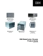
Brand: IBM Pages: 40

3130
Brand: H&S Pages: 32
CoreBuilder 9000
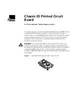
Brand: 3Com Pages: 8
CoreBuilder 9000
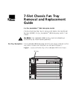
Brand: 3Com Pages: 12
Expansion Chassis
Brand: Dayna Pages: 7
ARX-2000
Brand: F5 Pages: 32
Viprion
Brand: F5 Pages: 74
RACK-360
Brand: IEI Technology Pages: 9
PAC-170
Brand: ICP Pages: 19
NI 9147
Brand: National Instruments Pages: 14
PXIe-1092
Brand: National Instruments Pages: 34
CompactDAQ cDAQ-9185
Brand: National Instruments Pages: 11
NI cDAQ-9181
Brand: National Instruments Pages: 4
PXI Series
Brand: National Instruments Pages: 11
SCXI-1000
Brand: National Instruments Pages: 60
Eight-slot USB Chassis NI cDAQ-9172
Brand: National Instruments Pages: 84

cDAQ-9179
Brand: National Instruments Pages: 108
cDAQ-9138
Brand: National Instruments Pages: 4


