


MODEL
S: LH-T3039X(LH-T3039, SH33SU-S/W) / LH-T3530X(LH-T3530, SH33SD-S/W)
SER
VICE MANU
AL
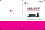
DVD/CD RECEIVER
SERVICE MANUAL
MODEL
S
:
LH-T3039X
(
LH-T3039
,
SH33SU-S
/W)
/
LH-T3530X
(
LH-T3530
,
SH33SD-S
/W)
Website http://biz.lgservice.com
Internal Use Only
LH-T3039X LH-T3530X
P/NO : AFN370644
24
MAY
, 2008