background image

Website http://biz.lgservice.com

Internal Use Only

Color Video Camera

SERVICE MANUAL

CAUTION

BEFORE SERVICING THE UNIT, READ THE “SAFETY PRECAUTIONS”
IN THIS MANUAL.

MODEL: L320-BN

MODEL:

L320-BN

SERVICE

MANUAL

P/NO : AFN75253068

OCTOBER, 2010

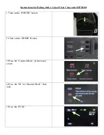
Summary of Contents for L320-BN
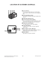
Page 1: ...z lgservice com Internal Use Only Color Video Camera SERVICE MANUAL CAUTION BEFORE SERVICING THE UNIT READ THE SAFETY PRECAUTIONS IN THIS MANUAL MODEL L320 BN MODEL L320 BN SERVICE MANUAL P NO AFN75253068 OCTOBER 2010 ...

Page 2: ... 3 10 COMPONENT REPAIR GUIDE 3 11 WAVEFORMS 3 13 WIRING DIAGRAM 3 15 BLOCK CIRCUIT DIAGRAMS 3 17 1 OVERALL BLOCK DIAGRAM 3 17 2 CCD BLOCK DIAGRAM 3 19 3 CCD CIRCUIT DIAGRAM 3 21 4 CSP BLOCK DIAGRAM 3 23 5 CSP CIRCUIT DIAGRAM 3 25 6 KEY IF BLOCK DIAGRAM 3 27 7 KEY CIRCUIT DIAGRAM 3 29 8 I F CIRCUIT DIAGRAM 3 31 9 POWER BLOCK DIAGRAM 3 33 10 POWER CIRCUIT DIAGRAM 3 35 CIRCUIT VOLTAGE CHART 3 37 PRIN...

Page 3: ...RRENT T V RECEIVERS IS THE PIC TURE TUBE HOWEVER THIS TUBE DOES NOT EMIT X RAYS WHEN THE HIGH VOLTAGE IS AT THE FACTORY SPECIFIED LEVEL THE PROPER VALUE IS GIVEN IN THE APPLICABLE SCHEMATIC OP ERA TION AT HIGHER VOLTAGES MAY CAUSE A FAILURE OF THE PIC TURE TUBE OR HIGH VOLTAGE SUPPLY AND UNDER CERTAIN CIR CUMSTANCES MAY PRODUCE RADIATION IN EXCESS OF DE SIRABLE LEVELS 2 ONLY FACTORY SPECIFIED C R ...

Page 4: ...etal pan els Input terminals Earphone jacks etc Electrostatically Sensitive ES Devices Some semiconductor solid state devices can be damaged easily by static electricity Such components commonly are called Electrostatically Sensitive ES Devices Examples of typical ES devices are integrated circuits and some field effect transistors and semiconductor chip components The following techniques should ...

Page 5: ...1 Vp p Composite 75 Ω Day Night Digital Day Night Auto Backlight OFF BLC HSBLC DNR 3D DNR Off Low Middle High Auto Gain Control Off Low Middle High Electronic Shutter Speed 1 50 to 1 90 000 1 60 to 1 90 000 Electronic Sensitivity OFF Auto White Balance Auto ATW One Push Manual User Color Mode STANDARD COOL WARM VIVID Power Source AC 24 V DC 12 V AC 24 V DC 12 V Power Consumption 2 9 W 2 9 W Operat...

Page 6: ...Lens iris output connector LENS This 4 pin connector is used to send the Iris control signal and power supply to an auto iris type lens E Setup menu control buttons Use these buttons to set the menu options F Power input terminal Supplies AC 24 V or DC 12 V from an external power source G Video output connector BNC type Supplies analog video signal composite to the con nected device such as a DVR ...

Page 7: ...1 6 ...

Page 8: ...ET MAIN CHASSIS CABINET AND MAIN FRAME VIEW CCD POWER IF 251 A43 257 A47 A49 263 262 261 264 KEY A48 250 4542 4545 4542 252 275 276 CABLE1 CABLE2 253 260 A40 265 4545 4545 4545 4568 4574 4574 4574 4574 4574 4542 4542 4542 ...

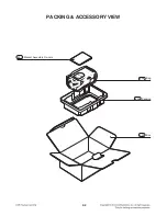
Page 9: ...2 2 801 Manual Assembly Owners 804 Bag 803 Packing 802 Box PACKING ACCESSORY VIEW ...

Page 10: ... WAVEFOM MONITOR VECTOR SCOPE TV or MONITOR CN601 WIRE 1 2m or above But when adjusting the iris keep tightly close with the viewer Yl Cy G Mg R B W CAMERA VIEW ANGLE Make the outer block full 1 TV or MONITOR 2 VECTOR SCOPE 3 WAVEFORM MONITOR 4 VIEWER 3200 K 5 LA100 LB140 LB200 FILTER 6 COLLIMATOR 7 DIGITAL EVR Equipment Initial Adjustment 8 PC Pentium or Higher ...

Page 11: ...AM DOWNLOAD DOWNLOAD METHOD ADJUSTMENT OBJECTIVE ERROR EQUIPMENT AND JIG ADJUSTMENT METHOD CAM EE TO SAVE THE MICOM PROGRAM TO MICOM NOT DOWNLOADED EFP RC JIG PC INTERFACE BOARD NUMBER OF MEASUREMENT LOCATIONS NUMBER OF ADJUSTMENT LOCATIONS ADJUSTMENT SPECIFICATION 1 Connect the PC with the downloading device 1 Connect the PC and EFP RC download device with the USB cable 2 When the device is conne...

Page 12: ...verXXXX hxw file and click on the Download button to download the file from the PC to the downloading device 4 And then download the LS900 s_verXXXX pbt file in the same method 4 Description of downloading device 1 There are following items on the LCD panel as shown below on the EFP RC downloading device 2 In the actual LCD panel only two lines will be shown but if you press the button the followi...

Page 13: ...n the download is completed the alarm will go off three times 8 When you see the V COMMAND OK message on the LCD panel the download is completed 5 Delete downloaded file 1 Place the cursor on the file to delete hxw or pdt and press the A button on the equipment 2 The screen will be displayed as follows 3 When you press the S button the file will be deleted A LS900 s_verXXXX hxw DELETE THIS FILE A ...

Page 14: ... Lens Select Switch to the bottom and check the screen 3 Error 1 Iris is full 2 The iris does not recover to normal screen after 3 seconds Iris is detected with delay 3 Iris does not open as black cap 4 Iris vibrates ADJUSTMENT OBJECTIVE ERROR EQUIPMENT AND JIG ADJUSTMENT METHOD CAM EE TO SAVE THE INITIAL PR VALUE ON MICOM PR NOT SET EFP RC JIG PC INTERFACE BOARD NUMBER OF MEASUREMENT LOCATIONS NU...

Page 15: ...stment method and precaution 1 Assemble the DC iris lens 2 Open adjustment jig program and connect the communication 3 Press the bad pixel correction button 4 When adjustment completion message is displayed proceed to the following process ADJUSTMENT OBJECTIVE ERROR EQUIPMENT AND JIG ADJUSTMENT METHOD CAM EE BAD PIXEL AUTO CORRECTION FUNCTION BAD PIXEL NOT CORRECTION WAVE FORM MONITOR MONITOR NUMB...

Page 16: ... and Key board tightly connected Check cable among ccd_csp and key and if board NO Is there any characters when Powered on Check if Flash rom in XDI is programmed NO Is non uniform scene on screen Check correct PR NTSC or PAL applied to XDI YES YES YES Replace power and key board Are outputs from power board Correct 15 V 7 5 V 5 V 3 3 V NO NO YES Replace CCD_CSP board L320 Replace CCD or CSP board...

Page 17: ...se Flash rom of XDI chip is not programmed Trouble shoot Download Flash rom data of XDI via E8a from PC Or Use Stand alone ROM downloader refer Download section of service manual 2 Symptom Effect Horizental glitches appears on screen Reason Ball grid of XDI IC is cracked from PCB Troubleshooting Change CCD_CSP board ...

Page 18: ...C2515 IC2502 NO Is the CSP VCC 3 3 V 1 8 V right Check the Power L2518 IC704 YES YES YES Check the IC703 Is the XRST right Check the X TAL X700 YES Is Frequency right Check the IC504 AFE YES Is VIDEO_IN0 11 right YES Check the CCD IC503 pin8 NO NO NO NO YES Check the IC706 Is Video out right NO TROUBLESHOOTING GUIDE ...

Page 19: ...L1105 NO Is the output of T1101 pin9 right Check the transformer T1101 NO YES YES Is the voltage of L2518 3 3 V right Check the IC2504 NO YES Is the voltage of L2515 7 V right Check the IC2503 NO YES Is the voltage of L2516 15 V right Check the IC2505 NO YES Is the voltage of IC2502 5 V right Check the IC2502 NO YES Replace component with trouble YES ...

Page 20: ...oblems occurs when you power on the unit 1 1 Solution Replace Fuse F1101 Bridge diode D1105 D1106 D1107 D1108 on power board 1 2 How to troubleshoot counter Measure Look at the physical of F1101 Look at the physical of D1105 D1106 D1107 D1108 Fuse Diode F1101 ...

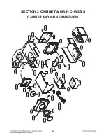
Page 21: ...3 12 ...

Page 22: ...C504 AFE pin13 ADCK 10 IC504 AFE pin14 PBLK 11 IC504 AFE pin15 HOBP 12 IC504 AFE pin16 SP1 13 IC504 AFE pin18 SP2 14 IC504 AFE pin20 CDS_IN 15 IC701 pinA20 XTAL_IN 16 IC701 pinF22 VIDEO OUT 17 Dual power CN5001 pin1 Video_out 18 Dual power L2515 7 V 19 Dual power L2516 pin1 15 V out 20 Dual power IC2504 pin8 LX 21 Dual power IC2502 pin1 5 V out 22 Dual power L2510 3 3 V out 2 CSP PART 3 POWER PART...

Page 23: ...01 BN BP CN2503 P9 5V SYNC_OUT AC24 DC12 AC24 DC12 CN803 SW IRIS_OUT 15 V 3 3 V 7 5 V CN2502 SW DAMP DRV 15 V 3 3 V 7 5 V CN5001 AC24 DC12V VIDEO_OUT 5V KEY BOARD IF BOARD 4p Harness JIG BD 10p B to B Connector E8A BD 15 Pin Harness 10p B to B Connector 5 Pin Harness CN2504 AC24 DC12V VIDEO_OUT 5 V WIRING DIAGRAM 3 15 3 16 ...

Page 24: ...UT CN703 KEY_UP KEY_DOWN KEY_RIGHT KEY_LEFT KEY_CENTER IRIS_SIG VIDEO_OUT 15V 3 3V 7 5V 5V 15 PIN HARNESS CN2502 KEY_UP KEY_DOWN KEY_RIGHT KEY_LEFT KEY_CENTER IRIS_SIG VIDEO_OUT 15V 3 3V 7 5V 5V CN5001 AC24 DC12 AC24 DC12 VIDEO_OUT 5V LED IF BOARD AC24 DC12 AC24 DC12 TM5001 AC24V DC12V AC230V 15V 3 3V 7 5V 5V KEY BOARD DUAL POWER BOARD 3 17 3 18 ...

Page 25: ...HT XH1 INVERTER RG INVERTER H1 INVERTER H2 XRG XH2 V1 V3 V2A V2B 3 3V 15V 7V 7V 15V 15V CCD_OUT CCD_OUT 3 3V 5V 3 3V 3 3V 3 3V 3 3V SUB IC503 ICX638 639 IC504 HD49343NP IC505 HT82V805 IC502 74LVC1G14 IC501 74LVC1G14 IC500 74LVC1G14 VL RG H1 H2 VIDEO_IN0 VIDEO_IN1 VIDEO_IN2 VIDEO_IN3 VIDEO_IN4 VIDEO_IN5 VIDEO_IN6 VIDEO_IN7 VIDEO_IN8 VIDEO_IN9 VIDEO_IN10 VIDEO_IN11 POWER BLOCK CSP BLOCK V T U O C N ...

Page 26: ...3 CCD CIRCUIT DIAGRAM 5 6 7 8 1 2 3 4 14 13 12 11 10 9 A 1 2 3 4 5 6 7 8 9 10 11 12 B C D E F G H I J K L M N O P Q R S T CCD EBY60137805_1 2010 03 04 WAVEFORM 3 21 3 22 ...

Page 27: ...n Motor cont IC707 BH6578 FVM TR 3 3V 5V POWER BLOCK FUNCTION KEY Control Logic POW CMOS H Bridge 1 6 7 5 8 2 3 4 T S D PRE GND POW GND Reset IC Port P0 Port P1 Port P2 Port P3 Port P4 Port P5 Port P6 Port P7 Port P8 Port P9 Port P10 8 8 8 8 8 8 8 8 7 8 8 3 3V SDRAM MCU AFE Block VIDEO_IN0 IN11 SHD SHP HOBP PBLK CLPDM ADCK CDS_DAT CDS_CLK CDS_CS XH1 XH2 XRG XV1 4 XSG1 XSG2 XSHT X TAL V OUT DIGITAL...

Page 28: ...5 CSP CIRCUIT DIAGRAM 16 15 A 1 2 3 4 5 6 7 8 9 10 11 12 B C D E F G H I J K L M N O P Q R S T CSP EBY60137805_2 2010 03 04 WAVEFORM 3 25 3 26 ...

Page 29: ...C2504 15 V 7 V 5 V video 3 3 V CN2502 15pin Harness KEY_UP KEY_DOWN KEY_RIGHT KEY_LEFT KEY_CENTER VIDEO_OUT CN2504 5pin Harness Regulator IC2505 D D Conv IC2503 Regulator IC2502 IRIS AMP DRV DAMP DAMP 9 6 V CN2503 5pin B to B 3 27 3 28 ...

Page 30: ...7 KEY CIRCUIT DIAGRAM 18 19 20 22 21 A 1 2 3 4 5 6 7 8 9 10 11 12 B C D E F G H I J K L M N O P Q R S T KEY EBY60808901 2010 03 04 3 29 3 30 WAVEFORM ...

Page 31: ...8 I F CIRCUIT DIAGRAM A 1 2 3 4 5 6 7 8 9 10 11 12 B C D E F G H I J K L M N O P Q R S T I F EBY60809101 2010 03 04 17 3 31 3 32 WAVEFORM ...

Page 32: ...9 POWER BLOCK DIAGRAM SMD Switching TRANS Rectify ES1Dx4 AC24V 9 5 V PWM CONTROL DC9 40V IC1101 FA5511 SE1102 LTV817 FB insulation CN1101 5pin SHORT protection LL SYNC T1101 SYNC_OUT 3 33 3 34 ...

Page 33: ...10 POWER CIRCUIT DIAGRAM A 1 2 3 4 5 6 7 8 9 10 11 12 B C D E F G H I J K L M N O P Q R S T POWER EBY60809001 2010 03 04 3 35 3 36 WAVEFORM ...

Page 34: ...e volt IC2505 1 15 2 0 3 3 3 IC5101 1 0 49 2 0 23 3 0 05 4 0 5 3 16 6 3 15 8 7 NO Cir no SPEC Value Value Result Remark 1 C540 2 2uF 20V 20V 0V GND 7V OK L320 CCD_CSP 2 C1111 1000uF 50V 50V 12V GND 0V OK L320 BN BP 3 C2504 C2534 C2535 10uF 16V 16V 3 3V GND 0V OK L320 BN BP 4 C2504 10uF 16V 16V 3 3V GND 0V OK L320 BN BP CP 5 C109 82uF 16V 16V 9V GND 0V OK L320 CP 6 C106 22uF 35V 35V 17 7V GND 0V OK...

Page 35: ...PRINTED CIRCUIT BOARD DIAGRAMS 1 CCD CSP P C BOARD DIAGRAM TOP VIEW BOTTOM VIEW 3 39 3 40 2 KEY P C BOARD DIAGRAM TOP VIEW BOTTOM VIEW ...

Page 36: ...3 41 3 42 4 I F P C BOARD DIAGRAM 3 POWER P C BOARD DIAGRAM TOP VIEW BOTTOM VIEW TOP VIEW BOTTOM VIEW ...

Page 37: ...3 43 3 44 ...
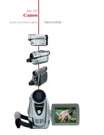
Reviews: