LG HT303SU, Service Manual
The LG HT303SU is a high-quality home theater system that offers an immersive audio experience. Enhance your movie nights with its powerful surround sound capabilities. To unlock the full potential of this product, easily download the user manual for free from our website. Never miss a beat or step in setting up your home theater system.
Share
Download


Reviews:
No comments
Related manuals for HT303SU
4155
Brand: NAD Pages: 14
AVN20D
Brand: Eclipse Pages: 86

3.0
Brand: Uconnect Pages: 44

MC 400
Brand: Magnat Audio Pages: 64
Criterion
Brand: National Pages: 14
CD1200
Brand: Eclipse Pages: 8
CD1200
Brand: Eclipse Pages: 101
MC 200
Brand: Magnat Audio Pages: 64

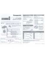
CQ-C1001W
Brand: Panasonic Pages: 2
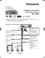
CQ-C1301NW
Brand: Panasonic Pages: 4
C5301W
Brand: Panasonic Pages: 18

C3303N
Brand: Panasonic Pages: 42
CQ-C5302W
Brand: Panasonic Pages: 38
CQ-C5355N
Brand: Panasonic Pages: 39
CQ-C8405N
Brand: Panasonic Pages: 66
CQ-CM130AU
Brand: Panasonic Pages: 2
CQ-RX460W
Brand: Panasonic Pages: 2
CQ-DX100W
Brand: Panasonic Pages: 8


