background image


Model Description

MODEL

BRAND

Printing Specification

1. Trim Size (Format) : 

215mm x 280 mm

2. Printing Colors

Cover : 

LG COLORS

Inside : 

Black

3. Stock (Paper)

Cover : 

Snow White 150 g/

Inside : 

Snow White 100 g/

4. Printing Method : 
5. Bindery  : 

Saddle stitch

6. Language : 

English

7. Number of pages : 

28 

( Including blank 3pages)

Part No.

1.

2

.

Service Guide Specification

Service Guide Specification

Changes 

4.

REV.

NO.

MM/DD/YY


CHANGE NO.

CHANGE    CONTENTS

1

2

3

4

5

7

6

SUFFIX


L1710SM

ALEUR

LG

3828TSL084E


(1) Origin Notification

* LGEDI : Printed in Indonesia 

* LGEWA : Printed in U.K.

* LGESP : Printed in Brazil        

* LGEMX : Printed in Mexico

* LGENT : Printed in China        

* LGEIL : Printed in India

8

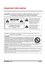
Special Instructions

3

.

Product Name

FLATRON L1710S

Summary of Contents for Flatron L1710S

Page 1: ...guage English 7 Number of pages 28 Including blank 3pages Part No 1 2 Service Guide Specification Service Guide Specification Changes 4 REV NO MM DD YY CHANGE NO CHANGE CONTENTS 1 2 3 4 5 7 6 SUFFIX L1710SM ALEUR LG 3828TSL084E 1 Origin Notification LGEDI Printed in Indonesia LGEWA Printed in U K LGESP Printed in Brazil LGEMX Printed in Mexico LGENT Printed in China LGEIL Printed in India 8 Specia...

Page 2: ...Pagination sheet Pagination sheet Cover Front cover Inside Blank English Contents 2 English 3 English 4 English English Rear Cover English 23 English 24 English blank Rear cover Inside blank ...

Page 3: ...rvice com E mail http www LGEservice com techsup html CAUTION BEFORE SERVICING THE UNIT READ THE SAFETY PRECAUTIONS IN THIS MANUAL CHASSIS NO CL 61 MODEL L1710S L1710SM AL R AU R AD R AG R Same model for Service Same looking with new chassis Issue Date 2004 2 ...

Page 4: ... 1 ...

Page 5: ...en Composite Sync 3 2 Video Input Signal 1 Type R G B Analog 2 Voltage Level 0 0 71 V a Color 0 0 0 Vp p b Color 7 0 0 467 Vp p c Color 15 0 0 714 Vp p 3 Input Impedance 75 Ω 3 3 Operating Frequency Horizontal 30 83kHz Vertical 56 75Hz 4 Max Resolution Analog 1280 x 1024 75Hz 5 POWER SUPPLY 5 1 Power AC 100 240V 50 60Hz 1 0A 5 2 Power Consumption 6 ENVIRONMENT 6 1 Operating Temperature 10 C 35 C 5...

Page 6: ... such as pencil or pen as this may result in damage to the panel Protect the module from the ESD as it may damage the electronic circuit C MOS Make certain that treatment person s body are grounded through wrist band Do not leave the module in high temperature and in areas of high humidity for a long time The module not be exposed to the direct sunlight Avoid contact with water as it may a short c...

Page 7: ...V 60 0 806 768 3 6 29 H 60 123 1312 1024 16 96 176 V 75 029 800 768 1 3 28 H 68 681 1456 1152 32 128 144 V 75 062 915 870 3 3 39 H 61 805 1504 1152 18 134 200 V 65 96 937 900 2 4 31 H 63 981 1688 1280 48 112 248 V 60 02 1066 1024 1 3 38 H 79 976 1688 1280 16 144 248 V 75 035 1066 1024 1 3 38 Mode H V Sort 1 2 3 4 5 6 7 8 9 10 11 12 13 25 175 28 321 25 175 31 5 40 0 49 5 57 283 65 0 78 75 100 0 92 ...

Page 8: ... screen display 100 100 Bring up Contrast and Brightness adjustment When adjusting your display settings always press the AUTO SELECT button before entering the On Screen Display OSD This will automatically adjust your display image to the ideal settings for the current screen resolution size display mode The best display mode is 1280x1024 60Hz This feature lets you easily select the best desired ...

Page 9: ...d LCD Module Control Board J1 M M S T 9 1 5 1 J702 J705 J706 Main Board 6 WIRING DIAGRAM LG Philips Hydis CMO Module Connector Ass y P N 6631T20024B Connector Ass y P N 6631T20020Q Connector Ass y P N 6631T11012W ...

Page 10: ...7 Power Board LCD Module Control Board M M S T 9 1 5 1 J702 J705 J706 Main Board WIRING DIAGRAM AU Module Connector Ass y P N 6631T120024B Connector Ass y P N 6631T20020Q Connector Ass y P N 6631T11012W ...

Page 11: ... w w w w V V V V o o o o l l l l t t t t a a a a g g g g e e e e D D D D i i i i f f f f f f f f e e e e r r r r e e e e n n n n t t t t i i i i a a a a l l l l S S S S i i i i g g g g n n n n a a a a l l l l i i i i n n n n g g g g LIPS 5V 5V AC I nput 3 3V Reg Diode KDS184 5V 3 3V 12V R G B H V Sync 3 3V 2 5V 3 3V 2 5V BLOCK DIAGRAM ...

Page 12: ...rpolates input to 1280 X 1024 resolution signal and outputs 8 bit R G B signal to transmitter 2 Power Part This part consists of the one 3 3V regulator and two 2 5V drop diodes to convert power which is provided 12V 5V in Power board 5V is provided for LCD panel and Micom Also 5V is converted 3 3V by regulator and 3 3V is converted 2 5V by drop diode Converted power is provided for IC in the main ...

Page 13: ...gh a bridge rectifier and a bulk capacitor 3 Energy Transfer This part function is transfer the primary energy to secondary through a power transformer 4 Output rectifier and filter This part function is to make a pulse width modulation control and to provide the driver signal to power switch to adjust the duty cycle during different AC input and output loading condition to achive the dc output st...

Page 14: ... is available to LCD Monitor only 1 Port Setup a Copy UserPort sys file to c WINNT system32 drivers folder b Run Userport exe c Remove all default number d Add 300 3FF e Click Start button f Click Exit button 2 EDID Read Write 1 Run WinEDID exe 2 Edit Week of Manufacture Year of Manufacture Serial Number a Input User Info Data b Click Update button c Click Write button ...

Page 15: ...11 Figure 1 Cable Connection SERVICE OSD 1 Turn off the power switch at the front side of the display 2 Wait for about 3 seconds and press MENU POWER switch with 1 second interval 3 The SVC OSD menu contains additional menus that the User OSD menu as described below a MODULE To select applied module b NVRAM INIT EEPROM initialize 24C08 c ADC OFFSET The lowest value of input leves sets to digitally...

Page 16: ...UT A SHORT POINT AS OPENING EACH POWER LINE CHECK J705 VOLTAGE PIN5 PIN6 5V NO CHECK 5VS LINE OPEN CHECK CHECK U501 PIN 8 Voltage 5V NO NO NO CHECK U201 PIN 122 PULSE CHECK U201 CHECK 3 3V LINE CHECK X TAL IS U201 PIN114 3 3V VOLTAGE YES YES NO PROBLEM YES CHECK KEY CONTROL CONNECTOR ROUTINE YES ...

Page 17: ...NOT DISPLAYED CHECK LIPS J705 PIN5 PIN6 5V NO 1 CONFIRM BRIGHTNESS OSD CONTRL STATE 2 CHECK MICOM DIM ADJ PORT J705 PIN10 5V NO LIPS CHECK PULSE AS CONTACTING SCOPE PROBE TO CAUTION LABEL CONTACT PROBE TO CAUTION LABEL CAN YOU SEE PULSE AT YOUR SCOPE NO REPLACE CCFL LAMP IN THE LCD MODULE YES YES YES YES ...

Page 18: ...O CHECK U801 U201 PIN122 123 OSCILLATE AS 12MHZ CHECK CONNECTION LINE FROM D SUB TO U501 TROUBLE IN CABLE OR LCD MODULE YES YES YES 3 NO RASTER OSD IS NOT DISPLAYED MST9111B NO RASTER OSD IS NOT DISPLAYED U501 PIN43 IS 64KHz H SYNC PIN44 IS 60Hz V SYNC IS PULSE APPEARED AT SIGNAL PINS AT MODE 12 NO NO ...

Page 19: ... 16 4 TROUBLE IN DPM TROUBLE IN DPM TROUBLE IN U501 CHECK PC PC IS NOT GOING INTO DPM OFF MODE NO CHECK H V SYNC LINE NO YES YES CHECK R773 R775 SYNC CHECK U501 PIN 43 44 SYNC PULSE ...

Page 20: ... 17 EXPLODED VIEW 1 4 11 c 7 9 10 5 3 6 b a 2 2 1 M M ST 91 51 8 ...

Page 21: ...0EN05V5 AU TFT COLOR SXGA 250NIT GEN5 BACK COVER ASSEMBLY LB700G 3808TKL039A HF350U TILT SWIVEL ASSEMBLY LM805L HIPS NO USB SHIELD INVERTER LAMP WIRE LB700K METAL ASSEMBLY FRAME LPL HD 1710SL METAL ASSEMBLY FRAME L1710SL_CMO METAL ASSEMBLY FRAME L1710SL_AU PWB PCB ASSEMBLY POWER L1710SM POWER TOTAL LIEN CHANG M CHASSIS THE INTERGRATED LIPS FOR LPL CMO HD PWB PCB ASSEMBLY POWER 17 AUO M CHASSIS POW...

Page 22: ...K104CK56A 0 1UF 1608 50V 10 R TP X7R C735 0CK104CK56A 0 1UF 1608 50V 10 R TP X7R C760 0CE107EF610 100UF KMG RD 16V 20 FL BULK C801 0CK103CK51A 0 01UF 1608 50V 10 R TP B Y DATE 2004 2 6 S AL LOC NO PART NO DESCRIPTION SPECIFICATION C803 0CE107EF610 100UF KMG RD 16V 20 FL BULK C804 0CK104CK56A 0 1UF 1608 50V 10 R TP X7R C805 0CK104CK56A 0 1UF 1608 50V 10 R TP X7R C805 0CK105CD56A 1UF 1608 10V 10 R T...

Page 23: ... TP R703 0RJ0752D677 75 OHM 1 10 W 5 1608 R TP R706 0RJ0752D677 75 OHM 1 10 W 5 1608 R TP R708 0RJ4700D677 470 OHM 1 10 W 5 1608 R TP R709 0RJ1001D677 1K OHM 1 10 W 5 1608 R TP R716 0RJ4701D677 4 7K OHM 1 10 W 5 1608 R TP R717 0RJ4701D677 4 7K OHM 1 10 W 5 1608 R TP R720 0RJ0000D677 0 OHM 1 10 W 5 1608 R TP R722 0RJ1000D677 100 OHM 1 10 W 5 1608 R TP DATE 2004 2 6 S AL LOC NO PART NO DESCRIPTION S...

Page 24: ...SCHEMATIC DIAGRAM 21 1 SCALER 1 ...

Page 25: ... 22 2 MICOM ...

Page 26: ... 23 3 POWER ...

Page 27: ... 24 4 CONNECTOR JACKS ...

Page 28: ...Blank Page1 ...

Page 29: ...Blank Page2 ...

Page 30: ...Feb 2004 P NO 3828TSL084E Printed in Korea ...

Reviews: