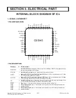
background image

MODEL 

:

FB163

U

(FBS163V)

SE
R

VICE MAN

U

AL

MINI HOME THEATER

SERVICE MANUAL

CAUTION

BEFORE SERVICING THE UNIT, READ THE “SAFETY PRECAUTIONS” IN THIS MANUAL.

MODEL : 

FB163

U

(FBS163V)

Website http://biz.lgservice.com

Internal Use Only

Summary of Contents for FB163U

Page 1: ...B163U FBS163V SERVICE MANUAL MINI HOME THEATER SERVICE MANUAL CAUTION BEFORE SERVICING THE UNIT READ THE SAFETY PRECAUTIONS IN THIS MANUAL MODEL FB163U FBS163V Website http biz lgservice com Internal Use Only ...

Page 2: ...SPECIFICATION 1 8 SECTION 2 EXPLODED VIEWS CABINET AND MAIN FRAME SECTION 2 1 DECK MECHANISM EXPLODED VIEW 2 3 SPEAKER EXPLODED VIEW 2 5 PACKING ACCESSORY VIEW 2 6 SECTION 3 ELECTRICAL PART INTERNAL BLOCK DIAGRAM OF ICs 3 1 AUDIO ELECTICAL PART 3 21 DVD ELECTICAL PART 3 31 WAVEFORMS OF MAJOR CHECK POINT 3 39 WIRING DIAGRAM 3 45 BLOCK DIAGRAMS 3 47 SCHEMATIC DIAGRAMS 3 47 PRINTED CIRCUIT BOARD DIAG...

Page 3: ...ely never be touched 4 Laser beams may damage the eyes Absolutely never permit laser beams to enter the eyes Also NEVER switch ON the power to the laser output part lens etc of the pick up if it is damaged 5 Cleaning the lens surface If there is dust on the lens surface the dust should be cleaned away by using an air bush such as used for camera lens The lens is held by a delicate spring When clea...

Page 4: ...ench should be covered with a conductive sheet and grounded When removing the laser pick up from its conductive bag do not place the pick up on the bag This is because there is the possibility of damage by static electricity 4 To prevent AC leakage the metal part of the soldering iron should be grounded 5 Workers should be grounded by an armband 1MΩ 6 Care should be taken not to permit the laser p...

Page 5: ...d as anti static can generate electrical charges sufficient to damage ESD devices 5 Do not use freon propelled chemicals These can generate electrical charges sufficient to damage ESD devices 6 Do not remove a replacement ESD device from its protective package until immediately before you are ready to install it Most replacement ESD devices are packaged with leads electrically shorted together by ...

Page 6: ...al Use Only THE STEPS FOR CHANGE THE OPTION CODE POWER ON Remote control 2 Front STOP push same timing during 5s Use arrow key to move to appropriate position and make changes Press pause key once Remote control 2 Front STOP push same timing during 5s Auto power off AUDIO MICOM OPTION NAME OPT 0 HEX 00 LED ...

Page 7: ... it press or DEMO again SET confirms the time you have selected when setting the clock RDS OPTIONAL shows infor mation about radio stations see listening to the radio USB connector Connect a remote USB compatible player here USB Rec USB DIRECT RECORDING EJECT Ejects or inserts the CD from the slot loader CD slot loader Do not push a disc forcibly Do not pull or push a disc while a disc is eject Pr...

Page 8: ...ervice purposes LGE Internal Use Only REMOTE CONTROL POWER MUTE FUNCTION INPUT SLEEP RETURN EQ EQUALIZER Effect VSM ECHO VOL MIC VOL SETUP MENU DISPLAY TITLE SELECT ENTER PRESET TUN PLAY STOP PAUSE STEP REC PROG MEMO VOLUME REPEAT CLEAR S TITLE VOCAL FADER RDS optional PTY optional ...

Page 9: ...quency 450 kHz Amplifier OUTPUT POWER 80 W 80 W 4Ω THD 0 5 Stereo Mode 80 W 80 W 4Ω THD 0 5 Frequency Response 40 20000Hz Signal to noise ratio 75dB DVD VCD CD player Frequency response audio 40 20000 Hz Signal to noise ratio audio More than 75dB 1 kHz Signal to noise ratio video More than 55dB 1 kHz Dynamic range audio More than 80dB Video output 1 0V p p 75Ω Component Video output Y 1 0V p p 75Ω...

Page 10: ...76 259 263 463 463 265 273 305 A44 272 452 463 463 463 463 463 463 463 463 274 455 SMPS FRONT MAIN A26 A47 A46 9701 CN101 CABLE2 CABLE1 A43 A46 262 J CABLE3 OPTIONAL PART 254 2 1 2 2 CABINET AND MAIN FRAME SECTION SECTION 2 EXPLODED VIEWS NOTES THE EXCLAMATION POINT WITHIN AN EQUILATERAL TRIANGLE IS INTENDED TO ALERT THE SERVICE PERSONNEL TO THE PRESENCE OF IMPORTANT SAFETY INFORMATION IN SERVICE ...

Page 11: ...11 014 013 016 015 010 024 025 024 025 024 025 024 025 035A 030 432 033 032 031 431 021 A30 035 435 036 2 3 2 4 Copyright 2008 LG Electronics Inc All right reserved Only for training and service purposes LGE Internal Use Only DECK MECHANISM EXPLODED VIEW ...

Page 12: ...8 LG Electronics Inc All right reserved Only for training and service purposes LGE Internal Use Only FRONT SPEAKER SPEAKER EXPLODED VIEW 850 852 863 851 853 855 A81 854 A80A 859 862 861 860 857 856 A80R A80L 864 854 A80 ...

Page 13: ...ll right reserved Only for training and service purposes LGE Internal Use Only Plug Ass y 1Way BLACK Antenna Loop 811 Battery 808 824 Antenna 825 Remote controller 900 Instruction Ass y 801 Packing 803 Box 802 Bag 804 PACKING ACCESSORY VIEW ...

Page 14: ...ol port interface Refer to the Recommended Operating Conditions for appropriate voltages RESET 6 Reset Input The device enters a low power mode when this pin is driven low AIN3A AIN3B 7 8 Stereo Analog Input 3 Input The full scale level is specified in the ADC Analog Characteristics specification table AIN2A AIN2B 9 10 Stereo Analog Input 2 Input The full scale level is specified in the ADC Analog...

Page 15: ...Input The full scale level is specified in the ADC Analog Characteristics specification table PGAOUTA PGAOUTB 28 29 PGA Analog Audio Output Output Either an analog output from the PGA block or high impedance See ìPGAOut Sour ce Select Bit 6 î on page33 VA 30 Analog Power Input Positive power for the internal analog section AGND 31 32 Analog Ground Input Ground reference for the internal analog sec...

Page 16: ...log Input 1 10 F 10 F 1800 pF 1800 pF 100 100 100 100 AIN1B Right Analog Input 1 AIN2A Left Analog Input 2 10 F 10 F 1800 pF 1800 pF 100 100 100 100 AIN2B Right Analog Input 2 AIN3A Left Analog Input 3 10 F 10 F 1800 pF 1800 pF 100 100 100 100 AIN3B Right Analog Input 3 AIN4A MICIN1 Left Analog Input 4 10 F 10 F 1800 pF 1800 pF 100 100 100 100 AIN4B MICIN2 Right Analog Input 4 AIN5A Left Analog In...

Page 17: ...ode Pump SMP connection to required external components in CY8C21634 part 7 IO M P3 1 In CY8C21434 part 7 Power Vss Ground connection in CY8C21634 part 8 IO M P1 7 I2C Serial Clock SCL 9 IO M P1 5 I2C Serial Data SDA 10 IO M P1 3 11 IO M P1 1 I2C Serial Clock SCL ISSP SCLK 12 Power Vss Ground connection 13 IO M P1 0 I2C Serial Data SDA ISSP SDATA 14 IO M P1 2 15 IO M P1 4 Optional External Clock I...

Page 18: ...rposes LGE Internal Use Only 3 DS8391 8390 SYSTEM BIOCK DIAGRAM ES8391 SDRAM VFD Driver TV Display Speakers Video EEPROM A V Receiver VFD Panel Microphone In S PDIF ROM Flash Motor Driver OPU Motor DVD CD IR Remote 8 16 MB Audio Audio Flash Memory Cards HDD Phoenix II 4 IP9010 BIOCK DIAGRAM ...

Page 19: ... control 10 REV3 I Loading motor reverseinput 11 FWD3 I Loading motor forward input 12 SVCC Signal supply voltage 13 DO3 O CH3 driver output 14 DO3 O CH3 driver output NO SYMBOL I O DESCRIPTION 15 DO4 O CH4 driver output 16 DO4 O CH4 driver output 17 DO5 O CH5 driver output 18 DO5 O CH5 driver output 19 VCC2 Power supply voltage2 20 IN5 I CH5 input 21 IN4 I CH4 input 22 GND Ground 23 BIAS I Bias 2...

Page 20: ...3 7 Copyright 2008 LG Electronics Inc All right reserved Only for training and service purposes LGE Internal Use Only 5 LC87F5NC8AVU QIP PIN CONFIGURATION ...

Page 21: ...3 8 Copyright 2008 LG Electronics Inc All right reserved Only for training and service purposes LGE Internal Use Only 5 LC87F5NC8AVU QIP SYSTEM BIOCK DIAGRAM ...

Page 22: ...3 9 Copyright 2008 LG Electronics Inc All right reserved Only for training and service purposes LGE Internal Use Only 5 LC87F5NC8AVU QIP PIN DESCRIPTION ...

Page 23: ...3 10 Copyright 2008 LG Electronics Inc All right reserved Only for training and service purposes LGE Internal Use Only ...

Page 24: ... IN1 Vcc Vcc OUT1 IN1 IN2 Vcc Vcc IN IN OUTPUT SYMBOL RATINGS UNIT PARAMETER Supply Voltage V V 18 V Input Voltage VIC 5 V Differential Input Voltage VID 30 V Output Current Io 50 m A Power Dissipation PD 300 SOP 8 mW 800 DIP 8 250 TSSOP 8 Operating Temperature Range Topr 40 to 85 C Storage Temperature Range Tstg 40 to 125 C ABSOLUTE MAXIMUM RATINGS TA 25 C TEST CIRCUIT ...

Page 25: ...3 12 Copyright 2008 LG Electronics Inc All right reserved Only for training and service purposes LGE Internal Use Only 7 0IRH330800A SYSTEM BIOCK DIAGRAM TEST CIRCUIT ...

Page 26: ...7_P M SLRCK SBCK SSDIN 0 3 PWM_HP_R_P M PWM_HP_L_P M EPD_ENA PWM_SWL_P M MIC_LRCK MIC_BCK MIC_SDIN MIC_MCLK DMIX_MCLK OLRCK OBCK DMIX_SDOUT PLL_DVDD PLL_DVSS PLL_AVDD PLL_AVSS DVDD DVSS IO_VDD IO_VSS Power Supply Reset Power Down Internal Reset Serial Audio Output interface Automatic Gain Limiter Main Volume Trim Volume Bass Manager EQ Down Mixer Mixer Mic Input Processor Input Mapper Sample Rate ...

Page 27: ...WM6_P PWM6_M IO_VSS IO_VSS PWM1_P PWM1_M OVERLOAD IO_VSS IO_VSS SSDIN1 EXT_MUTE DVDD IO_VDD DVDD SSDIN0 MSDIN3 SSDIN2 SSDIN3 IO_VSS IO_VDD MIC_SDIN PWM_SWL_P PWM_SWL_M PWM_HP_L_P PWM_HP_L_M PWM_HP_R_M IO_VSS PWM7_P PWM7_M PWM8_P PWM8_M EPD_ENA TEST_MODE2 TEST_MODE1 IO_VSS DMIX_LRCK DMIX_BCK DMIX_SDOUT DMIX_MCLK 98 99 100 96 97 93 94 95 91 92 85 86 87 88 89 90 83 84 81 82 71 72 73 74 75 61 62 63 64...

Page 28: ...ver Grid Driver SG1 KS1 SG2 KS2 SG3 KS3 SG4 KS4 SG5 KS5 SG6 KS6 SG7 KS7 SG8 KS8 SG9 KS9 SG10 KS10 SG11 KS11 SG12 KS12 SG13 KS13 SG14 KS14 SG15 KS15 SG16 KS16 SG17 SG18 SG19 SG20 GR1 GR2 GR3 GR4 GR5 GR6 GR7 GR8 SG21 SG22 SG23 SG24 GR9 GR10 GR11 GR12 GR13 GR14 GR15 GR16 DIN DOUT CLK STB Serial Data Interface LED Driver Control Display Memory Timing Generator LED1 Key Matrix Memory K1 K2 ...

Page 29: ...KS3 SG4 KS4 SG20 SG21 SG22 SG23 SG24 GR16 GR15 GR14 GR13 GR12 GR11 PT6324 DIN DOUT STB K1 K2 LED1 OSC 12 13 14 16 17 18 19 20 21 22 23 24 25 26 15 SG5 KS5 SG6 KS6 SG7 KS7 SG8 KS8 SG9 KS9 SG10 KS10 SG11 KS11 SG12 KS12 SG13 KS13 SG14 KS14 SG15 KS15 SG16 KS16 SG 17 39 38 37 36 35 34 33 32 31 29 27 28 30 SG18 SG19 52 50 49 48 47 46 45 44 43 42 41 40 51 GND VDD VEE GR1 GR4 GR5 GR6 GR7 GR8 GR9 GR10 GR2 ...

Page 30: ...tted at the falling edge of the shift clock starting from the lower bit 2 STB I Serial Interface Strobe Pin The data input after the STB has fallen is processed as a command When this in is ìHIGHî CLK is ignored 3 LED1 O LED Output Pin 4 K1 to K2 I Key Data Input Pins The data inputted to these pins is latched at the end of the display cycle 5 6 OSC I Oscillator Input Pin A resistor is connected t...

Page 31: ..._C BST_D RESET_AB RESET_CD System Power Supply Hardwire Mode Control PVDD GVDD 12 V VDD 12 V GND Hardwire OC Limit M1 M3 PVDD Power Supply Decoupling 35 5 V 12 V GND VAC PWM_A PWM_C PWM_D PWM_B VALID M2 Left Channel Output Right Channel Output Input H Bridge 1 Input H Bridge 2 GVDD VDD VREG Power Supply Decoupling 4 4 4 Bootstrap Capacitors 2nd Order L C Output Filter for Each Half Bridge Output H...

Page 32: ...e Drive PWM Rcv Overload Protection Isense GVDD_D RESET_CD 4 Protection and I O Logic PWM_C OUT_C GND_C PVDD_C BST_C Timing Gate Drive Ctrl PWM Rcv GVDD_C PWM_B OUT_B GND_B PVDD_B BST_B Timing Gate Drive Ctrl PWM Rcv GVDD_B PWM_A OUT_A GND_A PVDD_A BST_A Timing Gate Drive Ctrl PWM Rcv GVDD_A Ctrl BTL PBTLConfiguration Pulldown Resistor BTL PBTLConfiguration Pulldown Resistor BTL PBTLConfiguration ...

Page 33: ...3 20 Copyright 2008 LG Electronics Inc All right reserved Only for training and service purposes LGE Internal Use Only ...

Page 34: ...PART CHECK I OK OK NO NO NO Replace the related parts Check if output voltage of IC101 KIA7042 is 4 3V YES YES YES YES YES YES Check IC100 LC87F5NC8A 4 PIN power YES Refer to SMPS troubleshooting MICOM PART HECK I Check CN101 6PIN P SENS NO Check power of both terminals of IC101 KIA7042 Check if IC101 KIA7042 input is over 5V Check the related part of IC101 KIA7042 ...

Page 35: ...YES OK YES YES Check Q102 COLLECTOR YES Check the related part Replace the related parts Check the working condition X100 32 768kHz X101 9 8304MHz Check CN101 5PIN 5 6V Check power of both terminals of D101 RS1G YES NO Check Q10 EMITTER 5V and COLLECTOR 5V Check the related part MICOM PART CHECK II NO NO Replace the related parts Check Q102 BASE PIN 0 6V HIGH NO Check output power of IC101 KIA7042...

Page 36: ...raining and service purposes LGE Internal Use Only 3 IC103 S 24CS16A01 PART CHECK YES YES YES YES 81 PIN DATA 82 PIN CLK Check the related part NO Check MICOM power 5V CHECK IC100 LC87F5NC8A 81 82 PIN NO Replace the related parts NO Refer to micom troubleshooting OK OK ...

Page 37: ...ion condition and power F1 F2 both terminals over 3 7V Check powerVKK over 28V Check 4 5 PIN 5 6V YES Check IC304 PT6324 power 50 PINVKK 28V 9 52 PIN 5V YES YES Check power of each PIN IC100 Check IC304 Data communication PIN PIN 27PIN 3PIN STB 26PIN 2PIN DO 28PIN 1PIN CLK OK OK OK NO Replace the related part NO Replace the related part NO NO NO When 5V fails check D321SR35 input and output power ...

Page 38: ...put of line CLK R316 DATA R317 IC3A1 28PIN check 5V Check IC3A1 8Pin 9Pin IC100 97Pin CLK 96Pin DATA TOUCH PAD CHECK YES OK YES OK YES OK 6 PWM MODULATION PART CHECK Check PN102 10PIN 3 3V PWM MODULATION PART CHECK Refer to SMPS Troubleshooting NO Check if X701 12 288MHz is working YES YES YES YES Check IC702 PS9830 VDD PIN power 3 10 22 29 39 47 56 65 72 87 94 Check X701 2PIN 3 3V Replace the rel...

Page 39: ... 79 PIN CLK 96 PIN REST Check PWM MODULATOR output FL 75 74 R 71 70 OK Replace the related part NO Check resistance output of LINE DATA R797 CLK R795 RST R790 Refer to DVD Troubleshooting NO Check DVD ASS Y PS9830 communication condition P7403 YES OK Check IC702 PS9830 part Check resistance output of each LINE NO Check IC702 PS9830 DATA input OK YES YES YES Check IC702 PS9830 86 PIN CLK input Repl...

Page 40: ...S Troubleshooting PN102 3PIN 13 14 15 PIN 28V YES YES NO Check resistance power IC700 R702 701 726 727 724 Check input power of IC700 1 36 17 18 19 PIN 12V YES NO Replace the related parts Check output LINE COIL POWER AMP PART CHECK OK Check input power IC700 34 29 26 21 PIN YES Check PWM MODULATOR input 4 6 14 16 PIN YES Check POWER IC 700 34 29 27 20 PIN output ...

Page 41: ...rposes LGE Internal Use Only 8 TUNER FUNCTION PART CHECK YES YES NO Check TUNER MODUEL power Check 4PIN 9V CheckTUNER module TU100 is working YES NO Replace the related parts Check IC201 CS5345 14PIN output waveform TUNER FUNCTION PART CHECK OK Check IC201 CS5345 26 27PIN input waveform YES ...

Page 42: ...S Check BD901 LF901 902 NO Check short of P9702 line Check short of P9701 P9702 line NO Check short of P9701 line NO Replace IC901 902 Check the DC V of C905 if DC V is over 400V NO YES Check the DCV of C909 C903 C921 If DCV is in 14 19V And it is steady Check IC901 902 YES YES Check the DC V of C981 C945 If DC V is 6 1V YES Check the DC V of C950 C951 If DC V is in 29V OK MAIN PART MAIN PART ...

Page 43: ...S Check the PIN6 of P9702 if DCV is over 5 6V YES OK NO Check power circuit Troubleshooting YES VKK CHECK Check the PIN3 of P9702 if DCV is over 30V 1 YES OK 10 IPOD PART ONLY NORTH AMERICA YES YES YES YES YES NO Check the JK3C1 13pin 30pin Check the JK3C1 13pin and 30pin line LOADING NO Check the JK3C1 18pin 19pin Check theJK3C1 18pin and 19pin line OSD IPOD TURN ON IPOD OK OK YES OK YES ...

Page 44: ... TROUBLESHOOTING GUIDE 1 POWER CHECK GUIDE YES YES YES YES YES YES Does DVD appear at FLD Does No DISC or Time are appeared at FLD Check Connector P4405 P4407 P4408 NO NO Does it appear DVD ERROR at FLD POWER ON NO Check an Audio Micom Select the DVD Mode Reconnect it YES Check DVD MD Module Check the voltage of each pin on PN702 OK ...

Page 45: ...s between SDRAM IC502 ES8390 or the SDRAM is damaged YES SDRAM works properly NO Check the related circuit of ES8390 IC501 PIN80 83 84 85 YES ES8390VIDEO outputs properly NO NO Check the MD mecha Check the cable connection between DVD PCB and MD MECHA Does DISC was inserted inside when you push Disc1 5 button YES YES SW5 SW7 signals on PN4402 are OK NO Check the output signal of ES8390 to IC401 fo...

Page 46: ...nection with MECHA Do not put in disc and tray close Does the SLED move to inner side when it is at outer position YES YES Motor Drive DRV_MUTE pin is high YES YES SLED signal is OK NO NO Check Focus connection on ES8390 and motor driver IC Check cable connection with pick up head Optical Lens is moving for searching Focus YES YES Proper Focus outputs to motor driver NO Check the motor driver IC40...

Page 47: ...head Put disc in SLOT Laser turns on when reading disc YES YES DVDLD or CDLD output properly NO Check the related circuit of laser power transistor YES Collector voltage of power transistor is ok Q405 Q406 NO NO Check the SPINDLE related circuit on SLOT NO Laser off Check the cable connection between PN4401 and MD Does SPINDLE rotate YES YES YES Proper SPINDLE signal on ES8390 NO Check the SPINDLE...

Page 48: ...ween PN4401 and MD Focus On OK YES YES Proper signal on A B C D from MD NO Check the related circuit of ES8390 FOCUS signal YES Proper FOD signal on IC401 NO NO Check the related circuit between IC401 and ES8390 Check cable connection on pick up head Tracking OK YES YES YES Proper TRD signal on IC401 NO Check the Tracking control on motor driver IC401 T T output properly NO Check RF signal wavefor...

Page 49: ...O NO Check the SERIAL RESISTOR between ES8390 and IC702 YES Check the IC702 All outputs are Ok during playing DISK YES YES Audio signal data on ES8390 is OK NO For example composite video Check the video mute TR Q501 Output of Video buffer IC IC507 and ES8390 video signal data Picture signal data on ES8390 is OK D TEST END ...

Page 50: ...ck the POWER supply circuit Check PN102 Check the HRST signal Check the HRST signal Check the USB PART and DVD PART line Searching or USB Display check YES YES YES NO Check the USB JACK POWER supply Check PN205 Check the USB DATA LINE PN205 Reading OK check YES YES YES Check the ES8390 Check DATA LINE PIN 91 USB No 90 USB Po TURN ON USB OK ...

Page 51: ...3 38 Copyright 2008 LG Electronics Inc All right reserved Only for training and service purposes LGE Internal Use Only ...

Page 52: ...s Inc All right reserved Only for training and service purposes LGE Internal Use Only 1 WHEN POWER ON RESET DATA ETC WAVEFORM 1 RESET DVD 2 RX 3 TX 4 LCS3 FLASH Playing at USB function 1 HRST 2 5V 3 D 4 D WAVEFORMS OF MAJOR CHECK POINT ...

Page 53: ... right reserved Only for training and service purposes LGE Internal Use Only 2 OPEN CLOSE WAVEFORM AT POWER ON OPEN AND CLOSE 3 STARTING ACTION WAVEFORM IN MD DEVICE SLED HOME 1 Limit SW 2 OPEN 3 CLOSE 1 SLO from MPEG 2 SLED 3 SLED At Power on ...

Page 54: ...3 41 Copyright 2008 LG Electronics Inc All right reserved Only for training and service purposes LGE Internal Use Only 4 FOCUS WAVEFORM 1 FDO 2 F 3 F INSERT CD INSERT DVD 1 FDO 2 F 3 F ...

Page 55: ...08 LG Electronics Inc All right reserved Only for training and service purposes LGE Internal Use Only 5 AT POWER ON SPINDLE SIGNAL AT MD DECK 6 AT FIRST ACTION FOCUS SIGNAL A B C D 1 Spind 2 Spin 3 Spin 1 A 2 B 3 C 4 D ...

Page 56: ...3 43 Copyright 2008 LG Electronics Inc All right reserved Only for training and service purposes LGE Internal Use Only 7 TRACKING SIGNAL 8 RF WAVEFORM 1 Tro 2 Tr 3 Tr ...

Page 57: ...3 44 Copyright 2008 LG Electronics Inc All right reserved Only for training and service purposes LGE Internal Use Only 9 DISK TYPE JUGEMENT WAVEFORM DVD 1 F 2 FDO 3 SVRRF CD ...

Page 58: ...3 45 3 46 WIRING DIAGRAM Copyright 2008 LG Electronics Inc All right reserved Only for training and service purposes LGE Internal Use Only ...

Page 59: ...SPNN SPNP 2 LOAD SPIN SLED 6 RF PUDET F E A D C B LOAD_SW1 SW2 10 CD_DVDCT VC DVDMDI CDLDO DVDLDO 5 FR FR AMP_SD PROTECT PWM_CLK DAT RST AMP_PDN TUNER_DI DO CE MUTE RDS_CLK DAT BLUE TOOTH MODULE BT_LED BT_MPKEY VFD_DO VFD_STB VFD_CLK RCU TOUCH_CLK TOUCH_DAT STBY_LED KEY H P_SENS MIC_VOL MIC_DET MIC_SIG PORT_L R PORT_L R HP_L R HP_L R IPOD_RX IPOD_TX IPOD_LR IPOD_VIDEO IPOD IPOD_PWR IPOD_DET KEY2 I...

Page 60: ... NO CIR CUMSTANCES SHOULD THE ORIGINAL DESIGN BE MODIFIED OR ALTERED WITHOUT PERMISSION FROM THE LG CORPORATION ALL COMPONENTS SHOULD BE REPLACED ONLY WITH TYPES IDENTI CAL TO THOSE IN THE ORIGINAL CIRCUIT SPECIAL COMPONENTS ARE SHADED ON THE SCHEMATIC FOR EASY IDENTIFICATION THIS CIRCUIT DIAGRAM MAY OCCASIONALLY DIF FER FROM THE ACTUAL CIRCUIT USED THIS WAY IMPLEMENTATION OF THE LATEST SAFETY AND...

Page 61: ...ICOM SCHEMATIC DIAGRAM 2008 01 09 A 1 2 3 4 5 6 7 8 9 10 11 12 B C D E F G H I J K L M N O P Q R S T Copyright 2008 LG Electronics Inc All right reserved Only for training and service purposes LGE Internal Use Only ...

Page 62: ...AMP SCHEMATIC DIAGRAM 2008 01 09 A 1 2 3 4 5 6 7 8 9 10 11 12 B C D E F G H I J K L M N O P Q R S T Copyright 2008 LG Electronics Inc All right reserved Only for training and service purposes LGE Internal Use Only ...

Page 63: ...I O SCHEMATIC DIAGRAM 2008 01 09 A 1 2 3 4 5 6 7 8 9 10 11 12 B C D E F G H I J K L M N O P Q R S T Copyright 2008 LG Electronics Inc All right reserved Only for training and service purposes LGE Internal Use Only ...

Page 64: ...MPEG SCHEMATIC DIAGRAM 2008 01 09 A 1 2 3 4 5 6 7 8 9 10 11 12 B C D E F G H I J K L M N O P Q R S T Copyright 2008 LG Electronics Inc All right reserved Only for training and service purposes LGE Internal Use Only ...

Page 65: ...ERVO SCHEMATIC DIAGRAM 2008 01 09 A 1 2 3 4 5 6 7 8 9 10 11 12 B C D E F G H I J K L M N O P Q R S T Copyright 2008 LG Electronics Inc All right reserved Only for training and service purposes LGE Internal Use Only ...

Page 66: ...IPOD SCHEMATIC DIAGRAM 2008 01 09 A 1 2 3 4 5 6 7 8 9 10 11 12 B C D E F G H I J K L M N O P Q R S T Copyright 2008 LG Electronics Inc All right reserved Only for training and service purposes LGE Internal Use Only ...

Page 67: ...CART SCHEMATIC DIAGRAM 2008 01 09 A 1 2 3 4 5 6 7 8 9 10 11 12 B C D E F G H I J K L M N O P Q R S T Copyright 2008 LG Electronics Inc All right reserved Only for training and service purposes LGE Internal Use Only ...

Page 68: ...RONT SCHEMATIC DIAGRAM 2008 01 09 A 1 2 3 4 5 6 7 8 9 10 11 12 B C D E F G H I J K L M N O P Q R S T Copyright 2008 LG Electronics Inc All right reserved Only for training and service purposes LGE Internal Use Only ...

Page 69: ... MIC SCHEMATIC DIAGRAM 2008 01 09 A 1 2 3 4 5 6 7 8 9 10 11 12 B C D E F G H I J K L M N O P Q R S T Copyright 2008 LG Electronics Inc All right reserved Only for training and service purposes LGE Internal Use Only ...

Page 70: ...TOUCH SCHEMATIC DIAGRAM 2008 01 09 A 1 2 3 4 5 6 7 8 9 10 11 12 B C D E F G H I J K L M N O P Q R S T Copyright 2008 LG Electronics Inc All right reserved Only for training and service purposes LGE Internal Use Only ...

Page 71: ...cs Inc All right reserved Only for training and service purposes LGE Internal Use Only PRINTED CIRCUIT BOARD DIAGRAMS 1 SMPS P C BOARD DIAGRAM NOTE Warning Parts that are shaded are critical With respect to risk of fire or electrical shock ...

Page 72: ...3 73 3 74 2 1 MAIN P C BOARD DIAGRAM TOP VIEW Copyright 2008 LG Electronics Inc All right reserved Only for training and service purposes LGE Internal Use Only ...

Page 73: ...3 75 3 76 2 2 MAIN P C BOARD DIAGRAM BOTTOM VIEW Copyright 2008 LG Electronics Inc All right reserved Only for training and service purposes LGE Internal Use Only ...

Page 74: ...77 3 78 3 1 IPOD KEY P C BOARD DIAGRAM TOP VIEW Copyright 2008 LG Electronics Inc All right reserved Only for training and service purposes LGE Internal Use Only 3 2 IPOD KEY P C BOARD DIAGRAM BOTTOM VIEW ...

Page 75: ... Copyright 2008 LG Electronics Inc All right reserved Only for training and service purposes LGE Internal Use Only 4 1 I O P C BOARD DIAGRAM TOP VIEW 4 2 I O P C BOARD DIAGRAM BOTTOM VIEW 5 MIC P C BOARD DIAGRAM ...

Page 76: ...3 81 3 82 Copyright 2008 LG Electronics Inc All right reserved Only for training and service purposes LGE Internal Use Only 6 FRONT P C BOARD DIAGRAM ...

Page 77: ...CH KEY P C BOARD DIAGRAM BOTTOM VIEW 3 83 3 84 Copyright 2008 LG Electronics Inc All right reserved Only for training and service purposes LGE Internal Use Only 8 1 TOUCH SLIDE P C BOARD DIAGRAM TOP VIEW 8 2 TOUCH SLIDE P C BOARD DIAGRAM BOTTOM VIEW ...

Reviews: