background image

DVD RECORDER

SERVICE MANUAL

MODEL : DR165/DR175/DR676X

CAUTION

BEFORE SERVICING THE UNIT, READ THE “SAFETY PRECAUTIONS”
IN THIS MANUAL.

MODE

L

: DR165/DR175/DR676X

SE
R

VICE MANUAL

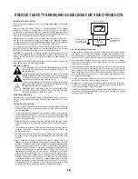
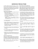
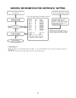
Summary of Contents for DR165

Page 1: ...DVD RECORDER SERVICE MANUAL MODEL DR165 DR175 DR676X CAUTION BEFORE SERVICING THE UNIT READ THE SAFETY PRECAUTIONS IN THIS MANUAL MODEL DR165 DR175 DR676X SERVICE MANUAL ...

Page 2: ...CONTENTS SECTION 1 SUMMARY SECTION 2 CABINET MAIN CHASSIS SECTION 3 ELECTRICAL SECTION 4 RS 01A LOADER PART SECTION 5 REPLACEMENT PARTS LIST ...

Page 3: ...GUIDELINES FOR VIDEO PRODUCTS 1 2 SERVICING PRECAUTIONS 1 3 General Servicing Precautions Insulation Checking Prodedure Electrostatically Sensitive Devices SERVICE INFORMATION FOR EEPROM IC SETTING 1 4 FLASH UPGRADE 1 5 LOADER UPGRADE 1 7 SPECIFICATIONS 1 9 ...

Page 4: ...lder splashes or sharp solder points Be certain to remove all loose foreign par ticles 4 Check for physical evidence of damage or deterioration to parts and compo nents for frayed leads or damaged insulation including the AC cord and replace if necessary 5 No lead or component should touch a high current device or a resistor rated at 1 watt or more Lead tension around protruding metal surfaces mus...

Page 5: ...ts including Metal pan els Input terminals Earphone jacks etc Electrostatically Sensitive ES Devices Some semiconductor solid state devices can be damaged easily by static electricity Such components commonly are called Electrostatically Sensitive ES Devices Examples of typical ES devices are integrated circuits and some field effect transistors and semiconductor chip components The following tech...

Page 6: ... OK EXIT MP MOVE EDIT MASK 00 EEP FF 0R D17 Each mask eeprom It shows a development release version EEPROM INITIAL SETUP is displayed in the field if pressing the Front PROG Key with the Remocon number clear key pressed in the status of powering on AUTO SEARCH is done since the initial screen of ACMS is serviced if powering on DETECT NEW EEPROM OPTION EDIT SCREEN OPTION condition of Present time t...

Page 7: ...Set 2 After Disc Reading you can see below screen 3 Press REC KEY 3 times It will start Inspection OPTIONAL PARTS DR100 8601 64M NTSC LG_DR100_8601NT64_UPDATE 590 DR100 860164M PAL LG_DR100_8601PAL64_UPDATE 590 DR100 860132M NTSC LG_DR100_8601NT_UPDATE 590 DR100 860132M PAL LG_DR100_8601PAL_UPDATE 590 DR100 8603 64M NTSC LG_DR100_8603NT_UPDATE 590 DR100 8603 64M PAL LG_DR100_8603PAL_UPDATE 590 exa...

Page 8: ...1 6 4 You can see both current and upgrade version Press REC KEY 5 Upgrading 6 After Upgrading you can see the below screen And automatically open tray Eject the Disc Reboot the set ...

Page 9: ...0 or JOLIET file system 2 Make a Volume label as DRIVE_UP 3 Write DvdSLXX rs1 YASMSLXX BIN on Root like below XX is Version 2 LOADER UPGRADE 1 Put Loader Upgrade Disc on Set 2 After Disc Reading you can see the below screen 3 Press REC KEY 3 times example Nero Burning Rom ...

Page 10: ... 4 After Tray open pick the disc up and close the tray 5 It shows both the current version and upgrade version Press REC KEY 6 Upgrading 7 After finishing Upgrade it shows the below screen and is tuned off ...

Page 11: ...D PCM 48 kHz 8 Hz to 22 kHz CD 8 Hz to 20 kHz DVD PCM 96 kHz 8 Hz to 44 kHz Signal to noise ratio More than 100 dB AUDIO OUT connector Harmonic distortion Less than 0 008 AUDIO OUT connector Dynamic range More than 95 dB AUDIO OUT connector INPUTS AERIAL IN Aerial input 75 ohms VIDEO IN 1 0 Vp p 75 ohms sync negative RCA jack x 2 SCART x 2 AUDIO IN 2 0 Vrms more than 47 kohms RCA jack L R x 2 SCAR...

Page 12: ...2 1 SECTION 2 CABINET MAIN CHASSIS CONTENTS EXPLODED VIEWS 2 2 1 Cabinet and Main Frame Section 2 2 2 Deck Mechanism Section RS 01A 2 3 3 Packing Accessory Section 2 4 ...

Page 13: ...22 463 463 251 275 275 280 452 452 452 251 300 463 A47 A60 A43 A44 A50 A46 A52 OPTIONAL PART CABLE9 CABLE5 CABLE3 CABLE1 SMPS JUNCTION MAIN I O TU701 A55 468 273 NOTES THE EXCLAMATION POINT WITHIN AN EQUILATERAL TRIANGLE IS INTENDED TO ALERT THE SERVICE PERSONNEL TO THE PRESENCE OF IMPORTANT SAFETY INFORMATION IN SERVICE LITERATURE A 5 4 3 2 1 B C D ...

Page 14: ...ECTION RS 01A 1034 1030 1025 1041 1432 1437 1434 1032 1033 1038 1011 1432 1020 1036 1432 Main C B A 1001 1431 1003 1002 1026 A001 A60 A002 1016 1433 1017 1013 1015 1012 1439 1047 1048 1046 1014 1018 1019 1043 1045 1044 1042 A005 ...

Page 15: ...ss y 1Way Plug Ass y 2Way Bag Packing Remote Control Instruction Ass y Packing Box 806 804 803 811 Plug Ass y 1Way 814 812 801 900 802 803 810 CABLE ASS Y 821 SCART CABLE FLAT CABLE 822 OPTIONAL PARTS 3 Packing Accessory Section 832 DISC ...

Page 16: ...24 4 VIDEO OUT BLOCK DIAGRAM 3 26 5 AUDIO IN BLOCK DIAGRAM 3 28 6 AUDIO OUT BLOCK DIAGRAM 3 30 7 SYSTEM MAIN BLOCK DIAGRAM 3 32 8 I O µ COM BLOCK DIAGRAM 3 34 9 SCART BLOCK DIAGRAM SCART MODEL ONLY 3 36 CIRCUIT DIAGRAMS 3 38 1 SMPS CIRCUIT DIAGRAM 3 38 2 MAIN POWER CIRCUIT DIAGRAM 3 40 3 MPEG CIRCUIT DIAGRAM 3 42 4 A LATCH FLASH DDR CIRCUIT DIAGRAM 3 44 5 LOADER DV CIRCUIT DIAGRAM 3 46 6 I O µ COM...

Page 17: ...ES YES YES YES Replace the R101 Is the D102 normal Check or Replace the D102 Replace the D123 Replace the IC103 Replace the IC102 Is the D121 Normal Is there about 2 5V at the IC103 Pin1 Is the IC102 Normal Replace the D124 Replace the D125 Is the D124 Normal Is the D125 Normal NO YES YES Replace the D127 Is the D127 Normal Power Line of I O PCB is short Is Vcc 10V 16V supplied to IC101 Pin7 1 POW...

Page 18: ...D127 NO Is the IC131 pin4 H YES Check the PWR CTL H signal from µ com NO Check or Replace the IC131 YES No 5V Is the Vcc 5 5V supplied to IC132 pin 1 YES Check or Replace the D125 NO Is the IC132 pin4 H YES Check the PWR CTL H signal from µ com NO Check or Replace the IC132 YES ...

Page 19: ...there about 12 5V at ZD151 Q164 Base YES Check Q164 and Replace NO Check D126 on SMPS Board and Replace NO Check Q162 and Replace NO Check the PWR CTL H signal from µ COM NO Is the VCC 33V supplied to Q162 Emitor YES Is there about 0V at Q162 Base YES Is there about 5V at R171 and 0 7V at Q156 Base YES Check Q156 and Replace YES ...

Page 20: ...TL H signal from µ COM NO Is there about 5V at R171 and 0 7V at Q156 Base YES Check Q156 and Replace YES No 5VT Is the VCC 5 3V supplied to Q155 Emitor YES Check 5 3VA on SMPS Board NO Is there about 0V at D152 and Q152 Collector YES Check Q155 and Replace NO Check the TIMER H signal from µ COM NO Is there about 5V at R180 and 0 7V at Q152 Base YES Check Q152 and Replace YES ...

Page 21: ...eck Q161 and Replace NO Check the TIMER H signal from µ COM NO Is there about 5V at R180 and 0 7V at Q152 Base YES Check Q152 and Replace YES No 5 0VD Is there about 5 3V at the IC153 pin 1 YES Check 5 3VA on SMPS Board NO Is there about 4V 5V at the IC153 pin 4 YES Check the PWR CTL H signal from µ COM NO Check the IC153 and Replace YES ...

Page 22: ... 4V 5V at the IC152 pin 4 YES Check the PWR CTL H signal from µ COM NO Check the IC152 and Replace YES No 2 5V Is there about 3V 3 8V at the IC151 pin 1 YES Check D154 and D127 on SMPS Board NO Is there about 4V 5V at the IC151 pin 4 YES Check the PWR CTL H signal from µ COM NO Check the IC151 and Replace YES ...

Page 23: ...V at R179 and R156 YES Check the STANBY H signal from µ COM NO Check Q158 and Replace YES No 1 8V SAA7137 Is the VCC 3 3V supplied to Q159 Emitor And IC154 pin 1 2 8 YES Check 3 3V power supply NO Is there about 3V 3 3V at Q159 Base and IC154 pin 3 YES Check Q159 and Replace NO Check IC154 and Replace YES ...

Page 24: ... NO Is there about 12 5V at ZD152 Q165 Base YES Check Q165 and Replace NO Check D126 on SMPS Board and Replace NO Check Q160 and Replace NO Check SW_5 3VA NO Is the VCC 33V supplied to Q160 Emitor YES Is there about 0V at Q160 Base YES Is there about 5 3V at Q166 Base YES Check Q166 and Replace YES ...

Page 25: ...upplied to Q154 Emitor YES Check D155 and 2 5V power supply NO Is there about 2V 2 5V at Q154 Base and IC154 pin 4 YES Check Q159 and Replace NO Check 3 3V power supply NO Is the VCC 3 3V supplied IC154 pin 1 2 8 YES Check IC154 and Replace YES ...

Page 26: ...13 IC 701 pin 19 R714 NO X1101 Clock oscillated 13 5MHz YES Replace X1101 NO Check IC1201 Flash Memory IC1101 NO IC1101 DEFECT NO IC1302 pin 26 Flash Chip Select YES R1126 R1127 I2C I F SCL SDA YES 4 DISC NOT RECOGNIZED Check Driver Power 5V 12V Check ATAPI Interface PML01 YES Change MEDIA TEST NO Check SMPS NO ...

Page 27: ... YES IC808 pin 15 18 Audio_out R L Is there a signal NO NO NO NO IC808 pin 14 19 Z_mute_R L IC701 pin 58 A_mute_L IC801 pin 1 7 Is there a signal IC803 pin 21 22 25 26 Is there a signal L806 L826 L825 L810 Is there a signal CHECK Cable connec tions TV Audio mute CHECK Q801 Q802 Q803 Q805 Q806 Q807 Q808 NO Replace IC801 CHECK IC803 pin 2 4 VCC 12V Pin 32 33 SCL SDA Replace IC803 YES NO CHECK IC801 ...

Page 28: ...OPTICAL DIGITAL OUTPUT CHECK PVM01 pin 1 SPDIF_OUT YES R851 Is there a signal YES YES YES CHECK JK803 pin 2 5 2V YES CHECK JK803 Optic cable connection YES C856 Is there a signal BD817 Is there a signal CHECK JK802 RCA cable connection ...

Page 29: ... P Model Only Without SCART Model YES YES CHECK IC 803 pin 2 4 VCC 12V Pin 32 33 SCL SDA CHECK IC1302 Reset Circuit NO IC1101 DEFECT NO CHECK IC901 power 3 3V 1 8V IC901 DEFECT Replace IC803 IC901 pin 34 Or R999 reset H YES X901 24 576MHz clock oscillated YES R902 R913 R997 R962 R978 I2C YES YES YES C901 pin 173 R903 Is there a signal When playing DISC no Audio output 7 NO TUNER AUDIO OUTPUT ...

Page 30: ...NO NO NO NO AV3 AV1 AV2 AV4 NO NO YES IC803 pin 10 16 Is there a signal YES YES YES YES YES YES YES C976 C977 Is there a signal YES NO IC901 pin 34 Or R999 reset H X901 24 576MHz clock oscillated C901 pin 173 or R903 CHECK IC901 power 3 3V 1 8V When playing DISC no Audio output IC901 DEFECT CHECK IC1302 Reset Circuit R902 R913 R997 R962 R978 I2C IC1101 DEFECT CHECK Cable connec tions Input signal ...

Page 31: ... SIGNAL WHEN PLAY DISC L1408 L1427 L1428 Is there a signal PVM01 pin 2 6 10 Is there a signal YES IC802 pin 18 21 24 Is there a signal YES CHECK IC802 pin 1 16 5 2V NO Replace IC802 CHECK SW801 status SW801 pin 2 RGB_SEL H YES YES ...

Page 32: ...05 L1406 Is there a signal PVM01 pin 14 18 22 Is there a signal IC803 pin 29 30 Is there a signal CHECK RCA S Video cable connection IC802 pin 27 30 32 Is there a signal NO NO YES NO YES YES YES YES SCART S Video RCA YES CHECK IC803 pin 2 4 VCC 12V Pin 32 33 SCL SDA Replace IC803 Replace IC802 CHECK SCART cable connection ...

Page 33: ...ignal of external input AV4 Composite S Video YES YES YES YES YES YES YES When Cable connecting Tuner and Rear SCART1 2 No TV video signal AV1 2 NO NO NO YES YES YES YES YES IC901 pin 34 Or R999 reset H X901 24 576MHz clock oscillated IC901 pin 108 or R930 VI_CLK CHECK IC901 power 3 3V 1 8V CHECK No RGB Component Composite S Video Signal when play DISC IC901 DEFECT CHECK IC1302 Reset Circuit C926 ...

Page 34: ...V mode Using Remote Control NO CHECK power 3 3V on I O board CHECK RESET circuit CHECK DV Cable Replace IC1601 IC101 DEFECT NO NO NO NO NO IC1601 pin 37 High X401 24 576MHz oscillated YES IC1601 pin 15 High Is there a signal YES IC1601 pin 1 27 28 29 30 Is there a signal YES IC1601 pin 2 3 Is there a signal YES Replace IC1601 YES ...

Page 35: ... C132 14VA 33VA 3 7VA R101 ERROR AMP IC103 6 4 10 11 13 2 1 Y CAP C110 Y CAP C111 12 9 7 8 FEED BACK BLOCK R121 R122 C131 R123 R124 R125 R126 RECTIFIER SMOOTING BLOCK D121 D122 BC131 R134 C135 C121 L121 C122 RECTIFIER SMOOTING BLOCK D124 C123 L122 C124 RECTIFIER SMOOTING BLOCK D128 C129 R127 R129 ZD151 5 3VA P CTL TO I O P101 BR BL BK WH C103 14 15 12V REG BLOCK IC131 C133 R130 5V REG BLOCK IC132 ...

Page 36: ...CT125 3 3V 5V L1114 XTAL_VDD 74LVC1G125 2 5V G2955 VTT 1 8V TSB41AB1 DMN8601 DMN8602 SDRAM 3V3A L1104 DAC_VDD L1109 USB_VDD L1105 REF_VDD L1105 PLL_VDD L1416 L1417 3V3D_E5 3V3D L1415 L1410 L1602 PLLVDD L1105 AVDD L1418 3V3D_PHY 2V5D_DDR L1413 L1409 74LVC1G125 ...

Page 37: ... Audio Processor SAA7137 Digital Vi deo ITU R BT 656 VIN_D 2 9 VIN_CLK PMV02 PVM01 CVBS Y C IC1803 AV S W MM1443 CVBS CVBS MAIN I O SCART AV1 SCART AV2 JK806 JK807 R G B CVBS JK802 TUNER TU701 AV4 In AV3 In RF In F_Y_IN F_C_IN F_CVBS_IN R_CVBS_IN R_SCART_IN R_SCART_IN R_SCART_IN EU2_V_IN SW_V_IOUT TU_V_IN EU1_V_IN ...

Page 38: ...MPEG ENC DEC DVD DRIVER ATAPI I F L C Filter 150 Ohm IC802 Video 6dB Amp BH7868FS CVBS S VIDEO Component RGB PMV02 PVM01 SW801 CVBS Y Pb Pr Y C IC1803 AV S W MM1443 CVBS R G B CVBS MAIN I O SCART AV1 SCART AV2 Y C CVBS Y G Pb B Pr R JK802 JK801 IC701 MICOM 5V GND ...

Page 39: ...l Audio IN MCLK I2S AI_SCLK AI_FSYNC AI_MCLK AI_DO IC901 Video Decoder Audio Processor SAA7137 L R IN JK804 JK805 L R IN TUNER TU701 AV4 In AV3 In RF In IC1803 AV S W MM1443 SCART AV1 SCART AV2 L R IN L R IN SIF I O IC903 904 AUDIO S W NJM2521 DAC SW_ AUDIO OUT L R IC_ OUT L R TU_ L R OUT F _ A L R IN R _ A L R IN SECAM AM ...

Page 40: ...al Audio IN MCLK I2S AI_SCLK AI_FSYNC AI_MCLK AI_DO IC901 Video Decoder Audio Processor SAA7137 L R IN JK804 JK805 L R IN TUNER TU701 AV4 In AV3 In RF In IC1803 AV S W MM1443 SCART AV1 SCART AV2 L R IN L R IN SIF I O IC903 904 AUDIO S W NJM2521 DAC SW_ AUDIO OUT L R IC_ OUT L R TU_ L R OUT F _ A L R IN R _ A L R IN SECAM AM ...

Page 41: ...V03 PVM02 RST_HOST RESET Circuit IC1301 Address Latch IC IC1302 FLASH ROM HD 0 15 HA 6 21 SYS_RST E5_RST SPI I F Buffer SPI_MISO SPI_CLK CS0 MOSI SIO_SPI_MISO SIO_SPI CLK CS0 MOSI IC901 SAA7137 AV IC IC808 CS4351 A DAC IC1601 TSB41AB1 PHY IC I2C SDA SCL RST_PHY VDEC_IRQ E5_ALE FCS0 OE2 FLASH_WE I O IC1202 IC1203 DDR SDRAM I F ...

Page 42: ...V S W IC803 MM1443 TU_L_OUT TU_R_OUT DRIVER IC601 PT6955 DIG601 LED CLOCK V_CLK VSTB TIMER_DOUT G 1 7 S 1 8 SIO_SPI_CLK SIO_SPI_MOSI SI0_SPI_CS0 SIO_SPI_MISO DMN8601 DMN8602 MPEG IC706 KIA7031 PWR_FAIL_L PWR_CTL_H SMPS POWER BOARD AV S W IC803 MM1443 VPS IC801 SDA5650 DAV TIMER_H CV IN2 AFT IC704 KIA7042 RESET SMPS Block on I O BOARD STANBY_H IC903 904 A S W NJM2521 IC_OUT_L IC_OUT_R SECAM_AM MAIN...

Page 43: ... SCART2 AUDIO DAC CS4351 A V 1 A V 2 SIF T Video SPI A V 3 A V 4 Rear RCA Front RCA Rear RCA SW A V D Audio ADC I2S D Audio DAC I2S D Video R 656 Coaxial OUT Optical OUT Rear RCA T Audio IEC60958 S PDIF CVBS S VIDEO Component Video 6dB Amp BH7868FS DV 1394 PHY TSB41AB1 TPA TPB Audio L R CVBS Audio L R CVBS CVBS S VIDEO Component ATAPI I F 3 36 3 37 ...

Page 44: ...ectricial shock A 1 2 3 4 5 6 7 8 9 10 11 12 B C D E F G H I J K L M N O P Q R S T IMPORTANT SAFETY NOTICE WHEN SERVICING THIS CHASSIS UNDER NO CIR CUMSTANCES SHOULD THE ORIGINAL DESIGN BE MODIFIED OR ALTERED WITHOUT PERMISSION FROM THE LG ELECTRONICS CORPORATION ALL COMPONENTS SHOULD BE REPLACED ONLY WITH TYPES IDENTICAL TO THOSE IN THE ORIGINAL CIR CUIT SPECIAL COMPONENTS ARE SHADED ON THE SCHEM...

Page 45: ...3 40 3 41 A 1 2 3 4 5 6 7 8 9 10 11 12 B C D E F G H I J K L M N O P Q R S T 2 MAIN POWER CIRCUIT DIAGRAM ...

Page 46: ...3 42 3 43 A 1 2 3 4 5 6 7 8 9 10 11 12 B C D E F G H I J K L M N O P Q R S T 3 MPEG CIRCUIT DIAGRAM ...

Page 47: ...3 44 3 45 A 1 2 3 4 5 6 7 8 9 10 11 12 B C D E F G H I J K L M N O P Q R S T A 4 A LATCH FLASH DDR CIRCUIT DIAGRAM ...

Page 48: ...3 46 3 47 A 1 2 3 4 5 6 7 8 9 10 11 12 B C D E F G H I J K L M N O P Q R S T 5 LOADER DV CIRCUIT DIAGRAM ...

Page 49: ...3 48 3 49 A 1 2 3 4 5 6 7 8 9 10 11 12 B C D E F G H I J K L M N O P Q R S T 6 I O µ COM CIRCUIT DIAGRAM ...

Page 50: ...3 50 3 51 7 TUNER MPX ADC DAC JACK CIRCUIT DIAGRAM A 1 2 3 4 5 6 7 8 9 10 11 12 B C D E F G H I J K L M N O P Q R S T ...

Page 51: ...3 52 3 53 8 DECODER CIRCUIT DIAGRAM A 1 2 3 4 5 6 7 8 9 10 11 12 B C D E F G H I J K L M N O P Q R S T ...

Page 52: ...3 54 3 55 9 TIMER CIRCUIT DIAGRAM 6 7 TOOL ONLY A 1 2 3 4 5 6 7 8 9 10 11 12 B C D E F G H I J K L M N O P Q R S T ...

Page 53: ...3 56 3 57 10 KEY CIRCUIT DIAGRAM 6 7 TOOL ONLY A 1 2 3 4 5 6 7 8 9 10 11 12 B C D E F G H I J K L M N O P Q R S T ...

Page 54: ... IC901 PIN108 27MHz PMV02 PIN05 AIN_FSYNC PMV02 PIN_FSYNC AOUT_FSYNC PMV02 PIN26 AOUT_D0 PMV03 PIN29 HOST_RXD PMV03 PIN26 HOST_TXD IC1202 PIN45 SDRAM_CLK1 PMV02 PIN18 VOUT_CVBS PMV02 PIN10 VOUT_G Y PMV02 PIN22 VOUT_C PMV02 PIN01 AOUT_IEC958 PMV02 PIN10 AIN_MCLKOUT PMV02 PIN07 AIN_SCLK PMV02 PIN29 VIN_D0 IC1601 24 576MHz PMV02 PIN2 VOUT_R Pr PMV02 PIN24 AOUT_MCLK ...

Page 55: ... 5 73 28 3 31 3 26 3 33 29 2 47 2 62 2 35 30 2 47 2 62 2 35 31 1 88 1 88 1 80 32 5 05 5 05 5 05 33 5 07 5 07 5 07 34 0 00 0 00 0 00 IC808_CS4351 1 1 61 1 61 1 62 2 1 62 1 62 1 61 3 1 62 1 62 1 62 4 1 63 1 63 1 63 5 3 17 3 17 3 17 6 0 00 0 00 0 00 7 3 08 3 08 3 08 8 3 03 3 03 3 03 9 3 23 3 23 3 23 10 3 21 3 20 3 20 11 3 22 3 22 3 22 12 1 25 1 25 1 25 13 4 12 4 12 4 12 14 12 12 12 12 12 12 15 4 11 4...

Page 56: ... 30 1 16 1 13 1 13 31 1 16 1 13 1 13 32 1 18 1 17 1 17 33 2 39 2 36 2 36 34 0 00 0 00 0 00 35 1 18 1 17 1 17 36 1 18 1 17 1 17 Q151_STB1132_5 2V E 5 27 5 27 5 27 C 5 21 5 21 5 21 B 4 52 4 52 4 52 Q155_KTA1271_5VT E 5 26 5 27 5 27 C 5 18 5 18 5 18 B 4 48 4 49 4 48 Q158_KTA1268_SW_5 3VA E 5 26 5 26 5 26 C 5 20 5 20 5 20 B 4 56 4 56 4 55 Q161_KTA1268_33VT E 33 90 33 90 34 00 C 33 80 33 80 33 90 B 33 ...

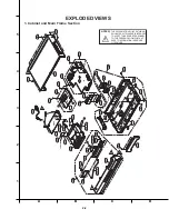
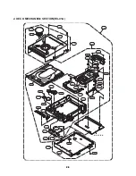
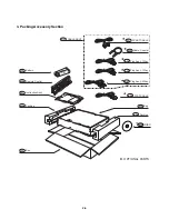
Page 57: ...3 64 3 65 PRINTED CIRCUIT DIAGRAMS 1 MAIN P C BOARD TOP SIDE ...

Page 58: ...3 66 3 67 2 MAIN P C BOARD BOTTOM SIDE ...

Page 59: ...3 68 3 69 3 I O P C BOARD TOP VIEW BOTTOM VIEW 4 JUNCTION P C BOARD TOP VIEW BOTTOM VIEW ...

Page 60: ...3 70 3 71 5 KEY P C BOARD TOP VIEW 6 7 TOOL BOTTOM VIEW 6 TIMER P C BOARD TOP VIEW 6 7 TOOL BOTTOM VIEW 7 POWER P C BOARD ...

Page 61: ...NGE 4 29 7 ATTACHMENT OPTICAL POWER MEASUREMENT 4 30 INTERNAL STRUCTURE OF THE PICK UP 4 31 1 BLOCK DIAGRAM OF THE PICK UP LPC 812R 4 31 2 PICK UP PIN ASSIGNMENT 4 32 3 SIGNAL DETECTION OF THE P U 4 33 DESCRIPTION OF CIRCUIT 4 34 1 ALPC AUTOMATIC LASER POWER CONTROL CIRCUIT 4 34 2 FOCUS TRACKING SLED SERVO CIRCUIT 4 35 3 SPINDLE SERVO CIRCUIT 4 37 MAJOR IC INTERNAL BLOCK DIAGRAM 4 38 LIC121 AN2211...

Page 62: ...he LIC201 LIC121 Does the pin 1 Reset of LIC271 change 0V to 3 3V at the power supply initial input mode Power Is the pin 5 of LIC401 3 3V Reference 1 65V VREF Check pin113 of LIC121 2 2V HDVREF Check pin78 of LIC121 NO NO YES YES YES YES Are the LX201 oscillating Check the LX201 16 9MHz Check the LIC201 NO Check the LIC401 NO Check the LIC121 NO Check it after connecting the power cable only on i...

Page 63: ...eck rotation After eject the tray Insert DVD R RW Disc and check rotation Does Disc rotate continuously and the drive recognize the disc Does Disc rotate continuously and the drive recognize the disc Go to Sled operating is abnormal Go to Laser operating is abnormal Go to Recognition fail Case1 CD ROM Disc Go to Recognition fail Case2 DVD Disc Go to Recognition fail Case3 Blank DVD R RW NO NO YES ...

Page 64: ...heck the connctor LPF303 Replace the LIC301 Check the connction of LIC201 pin 66 Replace the LIC201 Check the communication line between LIC201 NO YES YES YES NO Is there Tray drive voltage output LIC301 pin 1 2 Is there Tray control signal input LIC301 pin 46 YES Tray open doesn t work ...

Page 65: ... Is DRVMUTE2 signal H LIC301 pin 35 Check the LR316 LR317 Check the connection of LIC121 pin 32 Is there Sled drive voltage output LPM302 pin 1 2 3 4 Replace the Sled Motor YES NO NO YES YES Check the Connection LCN302 NO Is there Sled drive voltage input LIC301 pin 29 30 YES NO Is there Sled drive voltage output LIC301 pin37 38 39 40 YES NO ...

Page 66: ...ge output LIC301 pin 11 13 16 Is there Spindle drive voltage output LIC301 pin 1 2 3 Check the Connection LPM301 Replace the Spindle Motor NO NO NO YES YES Is there FG signal input LIC201 pin 71 NO YES YES Check the output of LIC301 pin 43 Check the connector LPM301 Replace the LIC301 Replace the LIC201 OK ...

Page 67: ... there Focus Search control signal input LIC301 pin5 Is DRVMUTE2 signal H LIC301 pin 35 Replace the LIC301 Check the connection LPM101 pin40 41 Check the connection of LIC121 pin 32 Replace the LIC121 NO YES Replace the Pick Up Is there Focus Search drive voltage output LIC301pin51 52 NO Check the connection of LIC201 pin 62 Check the communication line between LIC121 and LIC201 Replace the LIC201...

Page 68: ...21 NO Replace the LIC201 Check the Drive IC LIC301 and P U referring to Focus Actuator operating is abnormal Is there TDRV signal output in Tracking ON LIC201 pin66 NO Is PICK UP E F G H output normal LPM101 pin 8 5 9 4 YES YES NO LIC121 pin24 is MOUT1 FEP Monitor1 After disc recognition action Monitor port is off So please check TE signal during disc recognition ...

Page 69: ...e the Pick up Go to Focus Servo is unstable NO YES Does Focus Servo operate normally Check Pickup RF signal LIC121 Pin81 RFOUT was 2 2 5V NO Go to LD CHECK YES NO Replace LIC121 YES Check EQOUTP waveform LIC121 Pin 74 was 1 75 2 3V NO Go to Tracking Servo is unstable YES YES Check after replacing LIC201 It is OK NO OK ...

Page 70: ...ase 3 Blank DVD R RW Replace LIC201 Replace LIC121 YES NO NO Is there WBL LIC201 pin39 Signal YES NO Is there RF signal at LIC121 Pin81 YES Replace the Pickup NO Replace the LIC121 Is there RF signal at LIC121 Pin95 RFP and Pin96 RFN YES NO Replace the LIC201 Check again after the replace LIC121 It is OK OK Check the connection between LIC121 and LIC201 ...

Page 71: ...Go to Writing Part Check Remove the dust fingerprint and if the disc has long width scratch change it Check the media DVD R RW Does the disc have any dust scratch fingerprint Finalized Disc If DVD R disc use new DVD R disc If DVD RW disc erase the disc YES YES NO YES NO ...

Page 72: ...with DVD R RW disc Press the REC key Does writing finish without any error Is the written file read normally OK Eject tray Go to LD CHECK Is the re written file read normally Check and replace LIC201 LIC121 LIC101 YES YES YES YES NO NO ...

Page 73: ...ES check from How to use Test tool Execute C Laser Power Setup of How to use Test Tool Check reference voltage E F G FPD W1SET W2SET W3SET Is ALPC parameters valid Perform 5 Optical Power Setting OFF level W1SET level FPD W2SET level FPD W3SET level FPD OK N G OK NO OK OK OK N G N G N G ...

Page 74: ... How to use Test tool Select Mode DVD Test and perform Test from 4 LD Test of How to use Test tool Check the input of CD DVD pin 10 of LPM 101 Check the input of CD DVD pin 10 of LPM101 Check the input of W1SET pin 12 of LPM101 Check the input of FPD pin 126 of LIC121 END E ...

Page 75: ...e input of recording pulse pin 19 20 21 22 23 24 of LPM101 Check the input of FPD pin 126 of LIC121 END G Select Mode DVD Test and perform Test from 4 LD Test of How to use Test tool Check the input of CD DVD pin 10 of LPM101 Check the input of W3SET pin 14 of LPM101 Check the input of recording pulse pin 19 20 21 22 23 24 of LPM101 Check the input of FPD pin 126 of LIC121 END ...

Page 76: ...4 16 THE DIFFERENCE OF DVD R RW DVD R RW DISCS AND DVD ROM 1 RECORDING LAYER 0 74um 3T 0 4 um DVD ROM Read Only Disc DVD R RW Disc ...

Page 77: ...4 17 2 DISC SPECIFICATION 3 DISC MATERIALS 1 DVD ROM Single Layer Dual Layer ...

Page 78: ... a laser When a strong laser is applied to a disc the temperature of the organic dye material goes up the dye is decomposed and the substrate changes at the same time At this time a durable bit is created as is the case with a CD ROM Playback Signals are read with the differences of the reflection of a laser from pits 2 Recording format using organic dye material DVD R DVD R Disc structure Recordi...

Page 79: ...th a low reflection coefficient when it quickly cools off When a mid power laser is applied to heat gradually the recording material and then gradually cools it off it becomes crystal with a high reflection coefficient Playback A low power laser is used for playback The amount of reflected light depends on the status amorphous or crys talline of the recording material This is detected by an optica...

Page 80: ... for DVD RW has Type 1 and Type2 In Type 1 the mark with nT width is created by one top pulse and n 2 multi pulses Thus mark 3T is made by one top pulse and one multi pulse In Type 2 the mark with nT width is created by one top pulse and n 3 multi pulses Thus mark 3T is made by one top pulse only RL 02A uses MP type Write Strategy for DVD R and Type 1 for DVD RW as shown below Po Write Power Peak ...

Page 81: ...6mm Diameter 22mm 3th transition area Diameter 33mm Diameter 44mm 1th transition area 2th transition area Rim area Data Zone Lead in Zone Inner Drive Area Unrecorded Disc Outer Drive Area Inner Disc Test Zone in 27080H 28480H Information Zone Center hole Clamping Zone Diameter 120 mm Diameter 15mm Disc Center Diameter 16mm Diameter 22mm 3th transition area Diameter 33mm Diameter 44mm 1th transitio...

Page 82: ...ormed in IDT Zone 3 Layout of DVD RWdisc Data Zone Lead in Zone Unrecorded Disc Lead out Zone Inner Disc Test Zone in 2A7C80H 2DC80H Information Zone Center hole Clamping Zone Diameter 120 mm Diameter 15mm Disc Center Diameter 16mm Diameter 22mm 3th transition area Diameter 33mm Diameter 44mm 1th transition area 2th transition area Rim area 2A480H PSN Inner Disc Count Zone 30000H out Outer Disc Te...

Page 83: ...ibration Area in 203B0H 22F90H Unrecorded Disc Center hole Clamping Area Diameter 120 mm Diameter 15mm Disc Center Diameter 16mm Diameter 22mm 3th transition area Diameter 33mm Diameter 44mm 1th transition area 2th transition area Rim area Lead out Area 1E800H PSN RMA Recording Management Area 203C0H 22FA0H 30000H ...

Page 84: ...ing recommended ALPC Program in case of SVC OPTIONAL INSTRUMENT 1 USB ATAPI Interface if you don t have Notebook which has ATAPI Interface or use PC USB Port 2 Connector ATAPI Interface Board 2 ALPC PROGRAM Use the ALPC program in Dragon tool for Optical power setting It is consist of total 4 files Dragon_JW3P exe dragon cfg blue dat WNASPI32 DLL Four files must exist in same Directory Personal Co...

Page 85: ...gon_JW3P exe file 2 Enter the password It is qaz When you enter the password turn off the Caps lock in your keyboard 3 Set up the target device Press ATAPI button on the main dialog of Dragon tool And find the target device which is GDA 4164L ...

Page 86: ... the Alpc Opc menu CD DVD selection WriteScribe function don t use it Laser Read power on Laser off Erase power on multi pulse power on Non multi pulse power on WriteScribe function don t use it Set up the laset power parameter after finishing power measurement Laser power setup parameter ...

Page 87: ...on t watch light directly When you finish optical power measurement press button LD Off Press button save to ERPROM 2 CD LD Power Setting Select the CD in the Select Laser Diode Press Measure optical read Power Write Read Power value Press button save to ERPROM In case of CD power setting of RS 01A loader don t need to set up write power Although NMP MP Erase and HC power is N G when you press set...

Page 88: ...ptical power setting value Write optical Power Setting value to paper Adjust power setting again Compare original parameter to new parameter if parameter value is different highly original value is wrong or optical power may change But pick up LD test is all ok just adjust optical power setting again Normal range of ALPC parameter Optical power value which has been saved in the EEPROM ALPC Para 1 ...

Page 89: ...DVD R READ Reference DAC 40 145 2 DVD RW READ Reference DAC 40 145 3 VWDC1 30 100 4 VWDC1 Offset 0 20 5 VWDC2 40 140 6 VWDC2 Offset 0 20 CD 1 CD R READ Reference DAC 30 150 2 CD RW READ Reference DAC 80 250 3 VWDC1 10 39 4 VWDC1 Offset 0 20 5 VWDC2 20 57 6 VWDC2 Offset 0 20 ...

Page 90: ...ower is about 100mW Optical Power measurement method 1 Fit optical Power Meter λ wavelength value to DVD generally 660nm 2 DVD LD On 3 Approach power sensor to Pick up Lens about 3mm vertically Fix Lens and Sensor mark position 4 Read Monitor value move sensor read just a little and read max value caution unit is mW 5 Write monitoring value x 100 Only an integer 6 Fit opticcal Power Meter λ wavele...

Page 91: ... 9 EF3 10 C 11 D 12 SW PDIC 13 RF 14 RF 15 SW FM 16 VCC FM 17 GND FM 18 VREF FM 19 FM_OUT 20 TEMP 21 GND Themester 22 W1DISN 23 W1DIS 24 W2DISN 25 W2DIS 26 W3DISN 27 W3DIS 28 OSCEN 29 GND 30 GND 31 VCC 32 W3SET 33 W2SET 34 W1SET 35 RSET 36 OUTSET 37 ENABLE 38 VCC 39 GND 40 F Focus Actuator TILT TRACK 41 F 42 TILT 43 TILT 44 T 45 T 9 10 11 12 13 14 6 5 4 3 2 1 10 1 2 3 4 5 9 8 7 6 13 6 NE2 5 E2 4 E...

Page 92: ...3DISN LVDS control for output current Low Enable 25 W2DIS LVDS control for output current High Enable 24 W2DISN LVDS control for output current Low Enable 23 W1DIS LVDS control for output current High Enable 22 W1DISN LVDS control for output current Low Enable 21 GND FPD Ground connection for PDIC FPD TEMP 20 TEMP Output voltage for controlling temperature 19 FPD OUT APC amplifier output 18 VREF F...

Page 93: ...EF3 This signal is generated in RF IC LIC121 AN22113A and controls the pick up s left and right shift to find to track on Disc 3 RF Signal A B C D This signal is converted to DATA signal in DSP IC LIC201 MN103SA6G Pick Up module Photo Diode Tracking Focusing Infrared Iaser k F H E G A D B C A D B C k F H E G Offset TE Tp Sub2 Main Tp 2 Sub1 Track Center F E D C A B H G 3 SIGNAL DETECTION OF THE P ...

Page 94: ...SIGNAL IS INPUT FROM THE VREFPD PIN 124PIN THE ALPC BLOCK GENERATES THE SINGALS FROM THE INPUT LASER POWER SIGNALS IN THE FOLLOWING DETECTION SYSTEMS THIS BLOCK HAS FOUR DETECTION PATHS ALL AVERAGE VALUE PATH MULTI PULSE AVERAGE PEAK VALUE DETECTION PATH ERASE BOTTOM VALUE DETECTION PATH SPACE PLAYBACK POWER VALUE DETECTION PATH MN103SA6G Write Strategy LIC 201 LPM 101 Optical Pick up LPC 812R LD ...

Page 95: ...tor A B C D A B C D E F G H A B C D E F G H IC121 AN22113A FE TE LIC201 Servo Control MN103SA6G TE FE A D D A C SLED COMPENSATOR A D PARALLEL DIGITAL COMPENSATOR SDRV 60 64 66 67 STEP2 STEP1 LIC301 BD7956FS 29 30 M Stepping Motor Logic A 37 38 40 39 A B B Tracking Focusing Actuator T T F F 5 4 LEVEL SHIFT FDRV TDRV LEVEL SHIFT 53 54 51 52 Focus Tracking Sled Servo ...

Page 96: ...ERVO CIRCUIT 2 1 FOCUS TRACKING SLED SERVO PROCESS OPU PDIC S DPWM 10bit 100 50 MHz S DPWM 10bit 100 50 MHz ADC INT R On Off BD7956 Drive IC AN22113 FEP R On Off 16 bit Timer RFOUT Track Focus Internal u P F W Need to change to 16bit MN103SA6G MECHANISM ...

Page 97: ...SERVO CIRCUIT 3 1 SPINDLE SERVO PROCESS F E D C A B H G Pick up Wobble Signal Generator RF LIC121 AN22113A WBLIN EFM SRF SERVO DSP Phase Controller Frequency Controller 68 SPDRV LIC201 MN103SA6G LIC301 BD7956FS M Spindle Motor Level S hift ...

Page 98: ... VCC6 16 VHALF 17 CTC 18 CXDPH1 19 CXDPH2 20 MOUT2 25 GND1 26 PO0 27 PO1 28 PO2 29 PO3 30 PO4 31 PO5 32 PO6 33 STMOUT 39 TC 40 OFTR 41 BDO 42 VCC51 43 GND5 44 WTGT 45 PIO0 34 PIO1 35 PIO2 36 PIO3 37 FEPIDGT SH6 46 NC 47 WIDGT SH4 48 SH3 49 SH2 50 SH1 51 SH5 52 VCC4 53 SEN 54 SCK 55 SDAT 56 RSEN 57 RSDAT 58 VCC52 59 GND4 60 ASENV LPPM 61 LPPS 62 WBL 63 CLUMPGT 64 PAD0 65 PAD1 66 PAD2 67 PAD3 65 PAD...

Page 99: ...MC SMTEP SMTEN CHP0FT COFTR SLP14 SLP23 SMFEPN SSFEP SSFEPN SMTEP SMTEN SSTEP SSTEN SDAAOUT SDABOUT SDACOUT SDADOUT SDPDTEP SRFMA SRFMD SRFMB SRFMC SDPDTEN SPLAOUT SPLBOUT SPOF TCOP TCO TCON TIOP TIO SBDOAS TION VGA VGA COMP PK ENV PK ENV COMP VGA Bypass VGA Bypass M P X M P X DPD TE Dtetction TC TI Dtetction HDVREF VHALF VREF08 RFP CDRFP RFN CDRFN BDO RF OUT RFIN1 RFIN2 EQOUTP EQOUTN VREF GATE Al...

Page 100: ...AL BLOCK DIAGRAM LIC121 AN22113A FEP RF ANALOG SIGNAL PROCESSOR BLOCK DIAGRAM FEP LDD FEP DRC CD SERVO ADSC CD REC PERIPHERAL 32 bit CPU ANALOG CPU BCU FMT HOST 16 9MHz SDRAM 16 Mbit 64 Mbit Falsh ROM 2 Mbyte ECC HOST I F ...

Page 101: ...OL FG FG fin fin OSC 50k 47k 33 6k 33 6k 1 54 LDO ACO1 53 ACO1 52 ACO2 51 ACO2 50 ACO3 49 ACO3 48 AV 47 ACTIN3 46 LDIN 45 AGND 44 SPCNF 43 FG 42 V 41 fin 40 SLO1 39 SLO1 38 SLO2 37 SLO2 36 SLGND 35 CTL2 34 CTL1 33 SLRNF2 32 SLRNF1 31 SLVDD C M 30 SLIN2 29 SLIN1 28 DVcc 2 LDO 3 Vcc 4 ACTIN1 5 ACTIN2 6 TJMON 7 BTHC 8 SPVM_S 9 PGND1 10 PGND2 11 U 12 SPV 1 13 V M M 14 fin 15 PGND3 16 W 17 SPV 2 18 SPR...

Page 102: ......

Page 103: ...4 42 4 43 CIRCUIT DIAGRAMS 1 DSP CIRCUIT DIAGRAM A B C D E F G H I J K L M N O P Q R S T ...

Page 104: ...4 44 4 45 2 RF CIRCUIT DIAGRAM A B C D E F G H I J K L M N O P Q R S T ...

Page 105: ...4 46 4 47 3 DRIVE CIRCUIT DIAGRAM A B C D E F G H I J K L M N O P Q R S T ...

Page 106: ...1 1 3 29 2 0 00 3 3 28 4 0 00 5 4 99 6 0 00 7 0 00 8 4 98 9 0 00 10 4 99 11 0 00 12 0 00 13 0 00 14 4 99 15 0 00 16 1 09 17 3 28 18 0 00 19 4 99 20 0 00 21 0 00 22 0 00 23 0 00 24 0 00 25 0 00 26 0 00 27 0 00 28 4 97 29 0 00 30 3 29 31 0 36 32 0 00 1 0 00 2 0 00 3 1 69 4 1 64 5 1 66 6 2 67 7 2 60 8 0 00 9 0 00 10 1 65 11 0 00 12 0 25 13 1 58 14 1 82 15 2 20 16 3 29 17 1 65 18 1 56 19 0 00 20 2 50 ...

Page 107: ...4 50 4 51 PRINTED CIRCUIT DIAGRAMS 1 MAIN P C BOARD TOP VIEW ...

Page 108: ...4 52 4 53 2 MAIN P C BOARD BOTTOM VIEW ...

Reviews: