background image

SERVICE MANUAL

SERVICE MANUAL

CAUTION

BEFORE SERVICING THE UNIT, READ THE “SAFETY PRECAUTIONS”
IN THIS MANUAL.

Internal Use Only

Website http://biz.lgservice.com

JULY, 2015

MODEL: CM9750 (CM9750, CMS9750F)

MODEL: CM9750 

(CM9750, CMS9750F)


MINI HI-FI SYSTEM

P/NO : AFN77277023

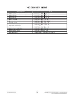
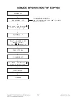
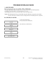
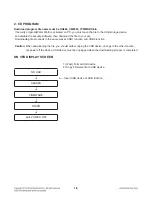
Summary of Contents for CM9750

Page 1: ...L CAUTION BEFORE SERVICING THE UNIT READ THE SAFETY PRECAUTIONS IN THIS MANUAL Internal Use Only Website http biz lgservice com JULY 2015 MODEL CM9750 CM9750 CMS9750F MODEL CM9750 CM9750 CMS9750F MINI HI FI SYSTEM P NO AFN77277023 ...

Page 2: ...CONTENTS SECTION 1 GENERAL SECTION 2 CABINET MAIN CHASSIS SECTION 3 ELECTRICAL SECTION 4 REPLACEMENT PARTS LIST 1 1 ...

Page 3: ...SECTION 1 SUMMARY CONTENTS SERVICING PRECAUTIONS 1 3 ESD PRECAUTIONS 1 5 HIDDEN KEY MODE 1 6 SERVICE INFORMATION FOR EEPROM 1 7 PROGRAM DOWNLOAD GUIDE 1 8 FOTA UPDATE 1 11 SPECIFICATIONS 1 12 1 2 ...

Page 4: ...age the eyes Absolutely never permit laser beams to enter the eyes Also NEVER switch ON the power to the laser output part lens etc of the pick up if it is damaged 5 Cleaning the lens surface If there is dust on the lens surface the dust should be cleaned away by using an air bush such as used for camera lens The lens is held by a delicate spring When cleaning the lens surface therefore a cot ton ...

Page 5: ... replacing a component part first disconnect the power supply lead wire from the unit 2 All equipment measuring instruments and tools must be grounded 3 The workbench should be covered with a conductive sheet and grounded When removing the laser pick up from its conductive bag do not place the pick up on the bag This is because there is the possibility of damage by static electricity 4 To prevent ...

Page 6: ...t to damage ESD devices 5 Do not use freon propelled chemicals These can generate electrical charges sufficient to damage ESD devices 6 Do not remove a replacement ESD device from its protective package until immediately before you are ready to install it Most replacement ESD devices are packaged with leads electrically shorted together by conductive foam aluminum foil or comparable conductive mat...

Page 7: ...Front Stop RMC 3 for 5s Clip Front Stop RMC Mute for 5s Disc Lock On Off Front Stop RMC Stop for 5s Power Disc Lock On Off Front Stop RMC EQ for 5s or Front Stop Front Open for 5s Demo All Key Lock On Off Front Stop RMC 9 for 5s BT Auto Power On Off Front RMC Power Key for 5s Child Safe On Off Volume 0 Min Front ENTER Key for 3s HIDDEN KEY MODE ...

Page 8: ...tatus too This is an example Front STOP Remote control push same timing during 5s FLD OP00 Move to appropriate position And make changes with RMC REPEAT key Press STOP Key VFD WRITE OK Front STOP Remote control push same timing during 5s VFD E2P CLR Completed 1 7 SERVICE INFORMATION FOR EEPROM ...

Page 9: ...ng file proceeds in the same way at USB1 function and USB2 function Caution When downloading the file you should neither unplug the USB device change to the other function nor power off the device USB device must be unplugged when the downloading process is completed ON VFD DISPLAY SCREEN 1 Fast Format USB device 2 Copy Firmware file to USB device NO USB Insert USB device at USB function SEARCH MI...

Page 10: ... Downloading file proceeds in the same way at USB1 function and USB2 function Caution When downloading the file you should neither unplug the USB device change to the other function nor power off the device USB device must be unplugged when the downloading process is completed ON VFD DISPLAY SCREEN 1 Fast Format USB device 2 Copy Firmware file to USB device NO USB Insert USB device at USB function...

Page 11: ...oading file proceeds in the same way at USB1 function and USB2 function Caution When downloading the file you should neither unplug the USB device change to the other function nor power off the device USB device must be unplugged when the downloading process is completed ON VFD DISPLAY SCREEN 1 Fast Format USB device 2 Copy Firmware file to USB device NO USB Insert USB device at USB function SEARC...

Page 12: ...1 11 FOTA UPDATE Step1 App connecting Check FW version Step3 Select update button Step2 Device version info Step7 FOTA complete Step4 Download from CDN server Step6 FW Flash Writing Step5 Transfer FW ...

Page 13: ...0 dB 600 Ω RCA jack L R PORT IN 1 2 Vrms 3 5 Ø jack MIC 27 mV CD Frequency Response 40 to 20 000 Hz Signal to noise ratio 75 dB Dynamic range 80 dB AMPLIFIER Total output 3 000 W FRONT 500 W x 2 4 Ω at 1 kHz WOOFER 1 000 W x 2 8 Ω at 70 Hz THD 25 FRONT SPEAKER Type Front 2 Way 2 Speaker Surround 1 Way 1 Speaker Impedance Front 4 Ω Surround 8 Ω Rated Input Power Front 500 W Surround 1 000 W Max Inp...

Page 14: ...SECTION 2 CABINET MAIN CHASSIS CONTENTS EXPLODED VIEWS 2 3 1 CABINET AND MAIN FRAME SECTION 2 3 2 MECHANISM DECK SECTION 2 5 3 PACKING ACCESSORY SECTION 2 7 4 SPEAKER SECTION 2 8 2 1 ...

Page 15: ...2 2 ...

Page 16: ... 263 265 265 443 CABLE2 272 252 252 A42 250 251 251 254 SMPS K 276 275 468 467 K 263 467 264 443 C D 498 498 271 498 271 271 271 467 270 A43 J 300 EXPLODED VIEWS 1 CABINET AND MAIN FRAME SECTION NOTES THE EXCLAMATION POINT WITHIN AN EQUILATERAL TRIANGLE IS INTENDED TO ALERT THE SERVICE PERSONNEL TO THE PRESENCE OF IMPORTANT SAFETY INFORMATION IN SERVICE LITERATURE ...

Page 17: ...1026 1439 A001 1002 1005 1001 1049 1437 1437 1024 1024 1030 1024 1043 1045 A005 A006 1016 1013 1015 1020 1024 1003 1439 1018 1019 1011 1012 1437 1004 2 MECHANISM DECK SECTION ...

Page 18: ...3 PACKING ACCESSORY SECTION 803 Packing 802 Box 804 Bag Packing 803 900 Remote Control 801 Owner s manual 808 Batteries Filter Ferrite Core 826A ...

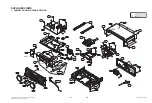
Page 19: ...4 SPEAKER SECTION A60L A60R ...

Page 20: ...C401 3 37 4 MOTOR DRIVER IC400 3 38 5 ADC IC201 3 39 6 USB CN502 3 39 7 BLUETOOTH CN504 3 40 WIRING DIAGRAM 3 41 BLOCK DIAGRAMS 3 43 1 SYSTEM BLOCK DIAGRAM 3 43 2 SMPS BLOCK DIAGRAM 3 45 3 POWER BLOCK DIAGRAM 3 47 CIRCUIT DIAGRAMS 3 49 1 SMPS POWER 1 CIRCUIT DIAGRAM 3 49 2 SMPS POWER 2 CIRCUIT DIAGRAM 3 51 3 MAIN CD DSP CIRCUIT DIAGRAM 3 53 4 MAIN ADC PWM CIRCUIT DIAGRAM 3 55 5 MAIN RF SERVO CIRCU...

Page 21: ... 2 Check if the bridge diode BD901 or BD902 is short circuit by over current with a digital multimeter 3 Check if the FET Q902 Q905 is normal or short If it is short condition it s destroyed Replace it with a new one Please replace 4 FET at the same time although several FET is OK 1 1 3 Service hint Any picture Remark F901 If F901 is not short circuit replace it with a same specifications one Q902...

Page 22: ... Check if the fuse F911 is open or short circuit 2 Check the Drain Source or Drain Gate Gate Source Resistance of Q911 Q914 with a digital multimeter If it is short condition it s destroyed Replace it with a new one Please replace 4 FET at the same time although several FET is OK 2 1 3 Service hint Any picture Remark F911 If F911 is not short circuit replace it with a same specifications one Q911 ...

Page 23: ... no 5 6 VA check the SMPS and if doesn t appear 3 3 V check IC505 2 Check 5 6 VA 12 V FL FL an 39 V when power on the set If the set doesn t work regardless of what the KEY2 changes high to low while pressing the power button X500 and X501 work normally but if you can not power on the set replace the IC501 with a new one on the MAIN board 3 1 3 Service hint Any picture Remark MAIN board top view M...

Page 24: ...m SMPS to VFD via the MAIN board 2 Check if the IC501 outputs VFD_RST VFD_CLK VFD_DO and VFD_STB to the FRONT board 3 Check if the VFD grid current amplifier circuit on the FRONT board Check the drive signal to the transistor s base If the control signals from VFD DGND_2 VH VDD isn t output replace VFD with a new one 4 1 3 Service hint Any picture Remark R327 TP304 Q301 Emitter about 30 Vp p FRONT...

Page 25: ...termeasure 1 Please check if this system is on bass blast mode C RL and RR make sound only on bass blast mode 2 Check the IC700 IC705 on your eyes 3 Check the audio signal output check pin13 of IC700 IC705 First Check the PWM Data input pin3 of IC700 IC705 4 If the audio signal output has no output try to change IC which has no output 5 Lastly check Speaker Terminal TM700 5 1 3 Service hint Any pi...

Page 26: ...tected Main reasons are like below When some of AMP FETs dead 6 1 3 Service hint Any picture Remark Notice for FET service In case of RF6775 Metal case FET Drain has electric potential So be careful when you deal with it You can see FET after removing heatsink Notice for Service Before repair Main Assy you need to discharge SMPS After then open the connector You should try to change both of FET an...

Page 27: ...and signal Check AMP IC Poor supply voltage Check SMPS Assy Poor signal Check PWM IC 2 Check CSD of FET driver IC IRS2092 EAN60778301 CSD has about 5 V on normal state When AMP has problem CSD is LOW state or keep change LOW to HIGH 7 1 3 Service hint Any picture Remark MAIN board top view MAIN board top view MAIN AMP circuit CN110 CN110 pin1 2 58 V pin1 2 58 V pin3 4 PGND pin3 4 PGND pin5 6 58 V ...

Page 28: ...05 pin3 on MAIN board If IC505 pin3 about 4 9 V D500 Input 5 6 VA doesn t come out check 5 6 VA from SMPS board 2 If IC505 pin3 about 4 9 V is normal check the PWR_CTRL IC505 pin2 is high about 3 3 V If PWR_CTRL isn t high check pin B2 of IC501 R524 R522 3 If PWR_CTRL is high check R524 and if there s no defective component then replace IC505 4 If 3 3 V VCC33 is normal check 1 2 V output pin2 volt...

Page 29: ... 2 2 How to troubleshoot Countermeasure 1 If 3 3 V 1 2 V is normal Check the CHIP_RESET of IC501 pin T12 on MAIN board If CHIP_RESET isn t high Check MICOM IC101 pin40 2 If CHIP_RESET is high Check the soldering status of 24 MHz crystal X500 3 If the crystal X500 doesn t oscillate Check R508 R509 C502 C503 around crystal X500 If there s no defective component then replace X500 8 2 3 Service hint A...

Page 30: ...w to troubleshoot Countermeasure 1 If the crystal X500 does oscillate Check Serial Flash IC503 on MAIN board Check 8pin VCC 6pin CLK 1pin CS 2pin DO 5pin DI of below waveform 2 If pin8 6 1 2 5 doesn t come out Check damping resistor R564 R563 R535 R536 R534 of IC503 If damping resistor of IC503 is OK then replace IC503 it need to download program 3 After change IC503 if It is still not below wavef...

Page 31: ...2 on MAIN board 8 4 2 How to troubleshoot Countermeasure 1 Check below waveform soldering status of SDRAM IC502 on MAIN board If pin17 CAS pin18 RAS pin19 CS pin38 CLK pin29 address pin2 DQ doesn t come out Check damping resistor R568 R570 R544 R547 2 If resistor is OK then replace IC502 SDRAM 3 After change IC502 if It is still not below waveform Check IC501 DSP IC 8 4 3 Service hint Any picture ...

Page 32: ...DSP IC501 8 5 1 Solution Please check and replace IC501 on MAIN board 8 5 2 How to troubleshoot Countermeasure 1 After check them by Previous pages about NO Booting if the set is still no booting Check soldering status of IC501 2 If below bootstrap waveform doesn t come out then replace IC501 DSP IC 8 5 3 Service hint Any picture Remark R594 PGPB12 Yellow R598 PAD19 Green R597 PAD20 Pink Bootstrap...

Page 33: ...l from pin16 of IC401 If no signal check 3 3 V RF and X400 2 Check the SPIN SPIN from IC400 to CN401 for driving SPINDLE motor It is about 3 6 Vp p If no signal check 7 V for IC400 3 Check if the FFC cable is solidly connected between CN401 and MD 4 Check the MD If the spindle motor is short circuit or has any trouble it can not rotate CD discs Please check the function after changing another MD 9...

Page 34: ...01 If no signal check 3 3 V RF and X400 2 Check the SLED SLED from IC400 to CN401 for driving SPINDLE motor It is about 2 9 Vp p If no signal check 1 8 V and 5 V for IC400 3 Check if the FFC cable is solidly connected between CN401 and MD 4 Check the MD If the sled motor is sort circuit or has any trouble it can not move the pickup module Please check the function after changing another MD 9 2 3 S...

Page 35: ...OAD from IC400 to CN401 for driving the tray open close motor It is about 3 85 Vp p If no signal check 5 V to IC401 If it has any trouble replace it with a new one 3 Check if the FFC cable is solidly connected between CN401 and MD 4 Check the MD If the tray motor is short circuit or has any trouble it can not open or close the tray Please check the function after changing another MD 9 3 3 Service ...

Page 36: ... a track on CD disc 1 Check the TRD signal from pin14 of IC401 If no signal check 3 3 V RF and X400 2 Check TR TR from IC400 to CN400 for driving the tracking actuator If no signal check 1 8 V and 5 V for IC400 3 Check if the FFC cable is solidly connected between CN400 and MD 4 Check the MD If the pickup module has any trouble it can not move the laser beam on the left or right side Please check ...

Page 37: ... the surface of a CD disc 1 Check the FDO signal from pin13 of IC401 If no signal check 3 3 V RF and X400 2 Check F F from IC400 to CN400 for driving the focusing actuator If no signal check 1 8 V and 5 V for IC400 3 Check if the FFC cable is solidly connected between CN400 and MD 4 Check the MD If the pickup module has any trouble it can not move the laser beam on the top or bottom side Please ch...

Page 38: ...ard IC312 on FRONT board 10 1 2 How to troubleshoot Countermeasure 1 Check 5 VU to FRONT board if 5 6 VA to pin2 of IC312 LDO doesn t come out check pin4 5 of CN314 if 5 6 VA is normal 5 VU of IC312 pin3 doesn t come out then replace IC312 2 Check Digital audio AMP block 10 1 3 Service hint Any picture Remark D D D D USB D D CN502 pin5 6 8 9 Waveform of USB D signal USB function signal flow ...

Page 39: ...l flow from IC501 to IC202 If there is any trouble check the power for each IC The power is normal but if the signal waveform to the IC is distorted or no signal replace it with a new one 5 Check if the digital audio AMP block is okay If AMP is damaged replace it with a new one 10 2 3 Service hint Any picture Remark AUX IC501 MLC3730 IC202 PS9860 PWM MCS_BCK MCS_LRCK IC201 CS5346 ADC MIC_DATA MCS_...

Page 40: ...K are entered from IC501 to IC201 5 Check if ADC_DATA is entered from IC201 to IC501 If no signal check 5 V 3 3 V ADC for IC201 If is NG replace it a new one 6 Check the following I2S signal flow from IC501 to IC202 If there is any trouble check the power for each IC The power is normal but if the signal waveform to the IC is distorted or no signal replace it with a new one 7 Check if the digital ...

Page 41: ... IC501 If no signal check 5 V 3 3 V ADC for IC201 If is NG replace it a new one 4 Check the following I2S audio signal flow from IC501 to IC202 If there is any trouble check the power for each IC The power is normal but if the signal waveform to the IC is distorted or no signal replace it with a new one 5 Check if the digital audio AMP block is okay If AMP is damaged replace it with a new one 10 4...

Page 42: ...CK MCS_MLCK MCS_LRCK is entered from IC501 to IC206 Check if MIC_DATA_IN is entered from pin9 of IC206 to pin T1of IC501 If no signal check 5 V 3 3 V for IC206 If it is abnormal change replace it a new one 5 Check the following I2S signal flow from IC206 to IC501 If there is any trouble check the power for each IC If the signals are abnormal replace it a new one 6 Check if the digital audio AMP bl...

Page 43: ... If there are no signal out from module replace new module 2 Check if BT_RX TX is entered from pin4 6 of CN504 to pin K1 L1 to IC501 DSP 3 Check the following I2S signal flow from IC501 to IC600 If there is any trouble check the power for each IC If the signals are abnormal replace it a new one 4 Check if the digital audio AMP block is okay If AMP is damaged replace it with a new one 10 6 3 Servic...

Page 44: ...e fuse Check or replace D962 Is D960 D961 normal Replace BD901 or BD902 Check P_CTL from μ com Check and replace IC951 Or check line of MAIN PCB is short or not Check or replace D960 D961 NO NO NO NO NO Is the F901 normal Is the VCC 13 VA supplied to IC951 pin2 Is the VCC 11 V 25 V supplied to IC901 pin4 Is BD901 or BD902 normal Is there H signal at IC951 pin1 ...

Page 45: ...or not Check or replace Q951 Is the VCC 7 VA supplied to IC953 pin2 Is there H signal at Q953 Base NO NO NO Is the R965 normal YES YES YES No output AMP gate line Check or replace R952 Check or replace D951 D952 Check and replace IC952 Or check line of MAIN PCB is short or not Is the VCC 14 VA supplied to IC952 pin1 to pin3 NO NO Is the R952 normal YES YES ...

Page 46: ...10 Check or replace IC902 and Check Q911 Q914 gate pin2 Components Resistors Diodes Q911 Q914 OK Replace Q911 Q914 Check or replace D953 D956 Check line of MAIN PCB is short or not Is the C903 C913 Voltage about 395 V Is F911 normal Is the PFC P CTL OK Is the AMP P CTL OK Is the VCC 12 V supplied to IC904 pin16 Is the VCC 12 V supplied to IC902 pin8 NO YES NO NO NO NO YES NO YES YES YES YES NO NO ...

Page 47: ...301 FL VKK voltage OK Replace LED LD311 LD313 LD301 LD303 Check MAIN board HELLO Display on MLD OK Top LED LD311 LD313 LD301 LD303 Turn on When turn the volume count is change NO NO NO NO NO NO NO NO NO CN605 cable connection OK CN605 pin24 12 V OK Check CN605 pin5 6 I2C data OK CN605 pin8 9 10 data signal OK CN605 pin14 15 16 24 power OK YES YES YES YES YES YES YES YES ...

Page 48: ...Check loading motor Check IC501 OPU driving Focusing Tracking OK Check OPU Pick up module Is motor impedance about 12 Ω IC401 pin34 35 36 I2S output signal OK Can disc insert IC501 pin N1 N2 N4 I2S input signal OK Disc reading OK NO NO NO NO NO NO NO NO NO IC401 RF Servo signal OK Focusing Tracking Sled signal OK LOAD OK YES YES YES YES YES NO YES YES YES A 3 NO AUDIO CHECK ...

Page 49: ...SB Power 5 VU OK YES A A When insert USB IC501 pin U7 U8 A7 A8 USB_D signal OK NO YES YES YES YES AUX FUNCTION Check audio cable Replace IC201 Check IC501 NO NO NO IC201 pin23 24 AUX input signal OK IC201 pin41 ADC_DATA_IN output signal OK IC201 pin42 43 44 I2S input signal OK ...

Page 50: ... R input signal OK IC201 pin41 ADC_DATA_IN output signal OK IC201 pin42 43 44 I2S input signal OK TUNER FUNCTION Check IC501 Replace IC201 Check 3 3 V of TU500 IC201 pin42 43 44 I2S input signal OK IC201 pin41 ADC_DATA_IN output signal OK NO NO NO TU500 TUNER_L R output signal OK YES A IC201 pin26 27 TUNER_L R input signal OK NO YES YES YES ...

Page 51: ...2 ELECTRICAL TROUBLESHOOTING GUIDE B A YES YES YES YES Check IC501 Replace IC202 Check IC501 NO NO NO IC501 pin D1 D2 E1 I2S Clock signal OK IC202 PWM data output signal OK IC501 pin E2 I2S data signal OK ...

Page 52: ...k SMPS Check Q717 Q718 pin47 50 of IC202 FL FR signal OK pin13 of IC700 IC701 IC702 IC703 FL FR audio signal OK IC203 IC204 FL FR audio signal OK 66 V 12 V 5 V Power voltage OK Q705 Q706 Q707 Q708 Q711 Q712 Q713 Q714 OK pin45 46 of IC202 SW1 signal OK pin13 of IC705 SW1 audio signal OK IC205 SW1 audio signal OK 66 V 12 V 5 V Power voltage OK Q717 Q718 OK NO NO NO NO NO NO NO NO NO NO YES YES YES Y...

Page 53: ...3 34 ELECTRICAL TROUBLESHOOTING GUIDE 4 NO LIGHTING SPEAKER LED YES YES Power on Check Q610 Q618 Q1103 Q1105 Check speaker Check IC601 NO NO White is turn on IC601 LED_5V OK ...

Page 54: ...3 35 WAVEFORMS OF MAJOR CHECK POINT 1 DSP IC501 X XI XO X XI XO Fig 1 2 Crystal of system 24 MHz Main DSP R508 R509 X500 Fig 1 1 Crystal of RTC 32 768 MHz R5D6 X501 2 1 3 4 4 3 2 1 ...

Page 55: ...3 36 2 PWM IC202 X XI XO Fig 2 2 DSP to PWM I2S IC202 pin26 30 Fig 2 1 Crystal 24 576 MHz IC202 pin4 5 X200 6 5 7 8 9 7 8 9 6 5 ...

Page 56: ...3 37 3 SERVO IC401 X XI XO Fig 3 2 CD 16M IC401 pin31 Fig 3 1 Crystal 16 9344 MHz X400 11 10 12 10 11 12 ...

Page 57: ...g 4 1 LO LO MOT_OPEN MOT_CLOSE for Driving TRAY Motor IC400 pin6 7 9 10 16 15 14 13 Fig 4 3 SP SP for Driving SPINDLE Motor IC400 pin17 18 20 19 Fig 4 2 SL SL for Driving SPINDLE Motor IC400 pin11 12 18 17 16 14 15 13 20 19 18 17 ...

Page 58: ...3 39 5 ADC IC201 6 USB CN502 Fig 6 USB D D CN502 pin5 6 8 9 Fig 5 ADC I2S IC201 pin42 43 44 23 21 22 24 25 24 25 21 22 23 ...

Page 59: ...3 40 7 BLUETOOTH CN504 B BT_TX BT_RX BT_RST BT_TX BT_RX BT_RST BT_TX BT_RX BT_RST Fig 7 BT_TX BT_RX BT_RST CN504 pin4 6 9 28 26 27 28 26 27 ...

Page 60: ...3 41 3 42 MAIN 33P 1 25mm 10P 1mm 6P 3 96mm 15P 2 5mm MD 10P 1 25mm FRONT FRONT_CTRL 6P 2mm 6P 2mm SMPS 6P 3 96mm 15P 2 5mm VFD Portable MIC 33P 1 25mm 10P 1 25mm Harness FFC WIRING DIAGRAM ...

Page 61: ...01 ADC CS5346 PRE AMP S4308 DAC PCM5101 PS9860 PWM E2PROM CLK DAT DRM_WEN CAS RAS SEL CLK CKE Speaker Lighting AMP_OSC ADC_DATA MCS_BCK LRCK MCLK EEPROM RL FL SW RR FR IR_IN_RL RL_OUT_P N FL_OUT_P N SW_OUT_P N RR_OUT_P N FR_OUT_P N M00_15 A00_16 SF_DI DO SF_CS SCK VFD_STB CLK DO RST VKK FL RMC MAIN VOL_A B KEY 1 2 SE OP_SW CL_SW UP_SW DN_SW D_SENSE MOT_MUTE CLOSE OPEN A B C D E F PD LD SPDO SLDO F...

Page 62: ... 14 VA 5 6 VA PVDD 58 V AC MAIN SMPS IC STR 2A153D Flyback MAIN TRANS u com BT USB MPEG FAN Mic Relay PFC P CTRL Half Bridge LLC TRANS AMP 5 V PVDD 58 V GATE Half Bridge LLC TRANS AMP Gate Drive 2 2 CH 3000 W OPAMP AMP P CTRL Totem pole PFC IC R2A20112A Interleaved CRM FET 20 A 600 V 4 EA Gate Drive PFC Out 395 V Ǹ Ǹ Ǹ Ǹ Ǹ Ǹ On Off On Off Ǹ Vcc Vcc On Off On Off Relay LED VFD Motor Drive 12 V Ǹ ...

Page 63: ...8 LDO AZ1117 Option 4 8 VA Bluetooth 5 V_AMP IC203 5 IC802 IC1000 1 OP AMP 6 AZ4580 IC700 5 IRS2092 6 AMP IC IC203 5 IC802 IC1000 1 OP AMP 6 AZ4580 IC700 5 IRS2092 6 AMP IC IRF6775M 12 FET IC600 TPS54331 9 V IC200 S4308 IC201 CS5346 FAN 2 GREEN LED 4 EA BLUE LED 4 EA IC312 A278R05 RMC RC311 IC311 VFD 2 mA 2 mA 80 mA 10 mA 38 mA 70 mA 22 mA 5 mA 6 mA 230 mA 2 2 mA 20 mA 2 mA 160 mA 20 mA 80 mA 15 m...

Page 64: ... IMPROVEMENT CHANGES INTO THE SET IS NOT DELAYED UNTIL THE NEW SERVICE LITERATURE IS PRINTED 1 Shaded parts are critical for safety Replace only with specified part number 2 Voltages are DC measured with a digital voltmeter during Play mode IMPORTANT SAFETY NOTE A 1 2 3 4 5 6 7 8 9 10 11 12 B C D E F G H I J K L M N O P Q R S T SMPS 1 2 EAX66225601_1 5 5 SD 1 2014 12 22 CAUTION Danger if fuse is i...

Page 65: ...ACTUAL CIRCUIT USED THIS WAY IMPLEMENTATION OF THE LATEST SAFETY AND PERFORMANCE IMPROVEMENT CHANGES INTO THE SET IS NOT DELAYED UNTIL THE NEW SERVICE LITERATURE IS PRINTED 1 Shaded parts are critical for safety Replace only with specified part number 2 Voltages are DC measured with a digital voltmeter during Play mode IMPORTANT SAFETY NOTE A 1 2 3 4 5 6 7 8 9 10 11 12 B C D E F G H I J K L M N O ...

Page 66: ...3 53 3 54 3 MAIN CD DSP CIRCUIT DIAGRAM 28 26 27 4 3 24 2 25 1 WAVEFORM NUMBER A 1 2 3 4 5 6 7 8 9 10 11 12 B C D E F G H I J K L M N O P Q R S T CD DSP EAX66215801_1 7 22 SD 1 2015 01 07 ...

Page 67: ...3 55 3 56 4 MAIN ADC PWM CIRCUIT DIAGRAM 21 22 23 7 8 9 6 5 WAVEFORM NUMBER A 1 2 3 4 5 6 7 8 9 10 11 12 B C D E F G H I J K L M N O P Q R S T ADC PWM EAX66215801_1 7 22 SD 2 2015 01 07 ...

Page 68: ...3 57 3 58 5 MAIN RF SERVO CIRCUIT DIAGRAM 10 11 12 16 14 15 13 20 19 18 17 WAVEFORM NUMBER A 1 2 3 4 5 6 7 8 9 10 11 12 B C D E F G H I J K L M N O P Q R S T RF SERVO EAX66215801_1 7 22 SD 3 2015 01 07 ...

Page 69: ...3 59 3 60 6 MAIN EXP VISENSE CIRCUIT DIAGRAM A 1 2 3 4 5 6 7 8 9 10 11 12 B C D E F G H I J K L M N O P Q R S T EXP VISENSE EAX66215801_1 7 22 SD 4 2015 01 07 ...

Page 70: ...3 61 3 62 7 MAIN AMP CIRCUIT DIAGRAM A 1 2 3 4 5 6 7 8 9 10 11 12 B C D E F G H I J K L M N O P Q R S T AMP EAX66215801_1 7 22 SD 5 2015 01 07 ...

Page 71: ...3 63 3 64 8 MAIN MIC AUX CIRCUIT DIAGRAM A 1 2 3 4 5 6 7 8 9 10 11 12 B C D E F G H I J K L M N O P Q R S T MIC AUX EAX66215801_1 7 22 SD 6 2015 01 07 ...

Page 72: ...3 65 3 66 9 FRONT CIRCUIT DIAGRAM A 1 2 3 4 5 6 7 8 9 10 11 12 B C D E F G H I J K L M N O P Q R S T FRONT EAX66215203_1 0 1 SD 2015 01 21 ...

Page 73: ...3 67 3 68 10 FRONT_CTRL CIRCUIT DIAGRAM A 1 2 3 4 5 6 7 8 9 10 11 12 B C D E F G H I J K L M N O P Q R S T CTRL_A EAX66233401_1 7 22 SD 2015 01 07 ...

Page 74: ...29 MAIN Pick up MD CN400 MAIN MD 8 DVCC_5V 5 5 01 5 01 MAIN FAN Module CN603 CN604 MAIN FAN Module 1 12 V 12 11 83 11 85 FRONT CTRL_A CN311 FRONT CN301 CONTROL 6 12 V 12 11 82 11 82 Location Value Capacitor u SPEC V 20 88 V 60 Hz 20 288 V 60 Hz Voltage V Voltage V C209 4 7 u 50 V 2 02 2 02 C226 100 u 16 V 11 31 11 32 C231 100 u 16 V 5 00 5 00 C238 220 u 16 V 3 30 3 30 C240 220 u 6 3 V 1 26 1 26 C3...

Page 75: ...3 71 3 72 PRINTED CIRCUIT BOARD DIAGRAMS 1 SMPS P C BOARD TOP VIEW ...

Page 76: ...3 73 3 74 SMPS P C BOARD BOTTOM VIEW NOTE Warning Parts that are critical with respect to risk of fire or electrical shock ...

Page 77: ...3 75 3 76 2 MAIN P C BOARD TOP VIEW ...

Page 78: ...3 77 3 78 MAIN P C BOARD BOTTOM VIEW ...

Page 79: ...3 79 3 80 3 FRONT P C BOARD TOP VIEW ...

Page 80: ...3 81 3 82 FRONT P C BOARD BOTTOM VIEW ...

Page 81: ...3 83 3 84 4 FRONT_CTRL P C BOARD TOP VIEW BOTTOM VIEW ...

Reviews: