background image

SERVICE MANUAL

SERVICE MANUAL

CAUTION

BEFORE SERVICING THE UNIT, READ THE “SAFETY PRECAUTIONS”
IN THIS MANUAL.

Internal Use Only

FEBRUARY, 2017

MODEL: CJ87 (CJ87, CJS87F)

MODEL: CJ87 

(CJ87, CJS87F)


MINI HI-FI SYSTEM

P/NO : AFN77612162

Summary of Contents for CJ87

Page 1: ...ANUAL SERVICE MANUAL CAUTION BEFORE SERVICING THE UNIT READ THE SAFETY PRECAUTIONS IN THIS MANUAL Internal Use Only FEBRUARY 2017 MODEL CJ87 CJ87 CJS87F MODEL CJ87 CJ87 CJS87F MINI HI FI SYSTEM P NO AFN77612162 ...

Page 2: ...CONTENTS SECTION 1 GENERAL SECTION 2 CABINET MAIN CHASSIS SECTION 3 ELECTRICAL SECTION 4 MECHANISM DM14B SECTION 5 REPLACEMENT PARTS LIST 1 1 ...

Page 3: ...PRECAUTIONS 1 3 ESD PRECAUTIONS 1 5 HIDDEN KEY MODE 1 6 1 HIDDEN KEY MODE TABLE 1 6 2 HIDDEN KEY MODE DESCRIPTION 1 7 SERVICE INFORMATION FOR EEPROM 1 9 PROGRAM DOWNLOAD GUIDE 1 10 FOTA UPDATE STEP USING BT APP 1 13 SPECIFICATIONS 1 15 1 2 ...

Page 4: ...age the eyes Absolutely never permit laser beams to enter the eyes Also NEVER switch ON the power to the laser output part lens etc of the pick up if it is damaged 5 Cleaning the lens surface If there is dust on the lens surface the dust should be cleaned away by using an air bush such as used for camera lens The lens is held by a delicate spring When cleaning the lens surface therefore a cot ton ...

Page 5: ... replacing a component part first disconnect the power supply lead wire from the unit 2 All equipment measuring instruments and tools must be grounded 3 The workbench should be covered with a conductive sheet and grounded When removing the laser pick up from its conductive bag do not place the pick up on the bag This is because there is the possibility of damage by static electricity 4 To prevent ...

Page 6: ...t to damage ESD devices 5 Do not use freon propelled chemicals These can generate electrical charges sufficient to damage ESD devices 6 Do not remove a replacement ESD device from its protective package until immediately before you are ready to install it Most replacement ESD devices are packaged with leads electrically shorted together by conductive foam aluminum foil or comparable conductive mat...

Page 7: ...Front Stop Remote Control Key Stop for 5s Front Stop Remote Control Key Stop for 5s Power Disc Lock On Off Front Stop Front Open for 5s Front Stop Front Open for 5s Demo ALL Key Lock Front Stop Remote Control Key 9 for 5s Front Stop Remote Control Key 9 for 5s BT Auto Power On Off Front Remote Control Key Power for 5s Front Remote Control Key Power SET Power Off ChildSafe On Off Volume 0 Min Front...

Page 8: ...rsion EQ Version EQ Check sum Version 2 2 EEPROM Initial Function Initialize data stored in EEPROM and BACKUP RAM data Entrance Key Front Stop Remote Control Key for 5s Exit Key Auto exit Explanation E2P CLR is displayed on the VPD and turn off the power automatically 2 3 OPTION EDIT EEPROM Refer to the page 00 2 4 APD Test Display Function Auto Power Down timer is displayed on VFD Entrance Key Fr...

Page 9: ...de all key blocks only the volume key is effective when All Key Lock is enabled To release Demo Mode it is available after All Key Lock Off 2 8 BT Auto Power On Off Function Ability to disable BT Auto Power On function by network shutdown regulation Entrance Key Front Remote Control Key Power for 5s Exit Key SET Power Off with Front Remote Control Key Power 2 9 ChildSafe On Off Function Power off ...

Page 10: ...Move to appropriate position And make changes with remote control REPEAT key Press Stop Key VFD WRITE OK Front Stop Remote control push same timing during 5 s VFD E2P CLR Completed 1 9 SERVICE INFORMATION FOR EEPROM NAME OPT0 OPT1 OPT2 OPT3 OPT4 OPT5 OPT6 OPT7 OPT8 OPT9 OPT10 OPT11 OPT12 OPT13 OPT14 DETECT NEW EEPROM OPTION EDIT SCREEN HEX 01 31 2D 26 19 00 00 43 4A 38 37 00 00 00 00 ...

Page 11: ... file proceeds in the same way at USB1 function and USB2 function Caution When downloading the file you should neither unplug the USB device change to the other function nor power off the device USB device must be unplugged when the downloading process is completed ON VFD DISPLAY SCREEN 1 Fast Format USB device 2 Copy Firmware file to USB device NO USB Insert USB device at USB function SEARCH MICO...

Page 12: ...ownloading file proceeds in the same way at USB1 function and USB2 function Caution When downloading the file you should neither unplug the USB device change to the other function nor power off the device USB device must be unplugged when the downloading process is completed ON VFD DISPLAY SCREEN 1 Fast Format USB device 2 Copy Firmware file to USB device NO USB Insert USB device at USB function S...

Page 13: ...et Downloading file proceeds in the same way at USB1 function and USB2 function Caution When downloading the file you should neither unplug the USB device change to the other function nor power off the device USB device must be unplugged when the downloading process is completed ON VFD DISPLAY SCREEN 1 Fast Format USB device 2 Copy Firmware file to USB device NO USB Insert USB device at USB functi...

Page 14: ...Device Version info on Setting tab Step3 Select update button When touch the Update button user could update the SET firmware using FOTA Step2 Device version info When touch the Device Version info button user could find the current and latest SET version on pop up menu Step4 Confirm update Select the OK button on the caution message ...

Page 15: ...omplete After completed the download from the smart phone the SET overwrite the firmware to flash memory When finishing the flash memory writing pop up message about finish is displayed and the SET auto power off Step6 Transfer FW After completed the download from server smart phone start to transfer the firmware to the SET The progress bar is displayed on BT App ...

Page 16: ...UNER FM Tuning Range 87 5 to 108 0 MHz or 87 50 to 108 00 MHz AM Tuning Range 522 to 1 620 kHz 520 to 1 710 kHz or 522 to 1 710 kHz SYSTEM Frequency Response 40 to 20 000 Hz Signal to noise ratio More than 75 dB Dynamic range More than 80 dB Bus Power Supply USB 5 V 500 mA AMPLIFIER RMS Output power Total output 2 350 W RMS HIGH 585 W RMS x 2 6 Ω at 5 kHz 30 THD LOW 590 W RMS x 2 6 Ω at 1 kHz 30 T...

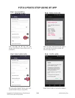
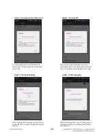
Page 17: ...1 16 ...

Page 18: ...RAME SECTION 2 3 2 PACKING ACCESSORY SECTION 2 7 3 SPEAKER SECTION 2 8 DISASSEMBLY INSTRUCTIONS 2 9 1 Case Top 2 9 2 Panel Front Assembly 2 9 3 Panel PCB Multi Knob 2 10 4 Bracket Hook 2 11 5 Main PCB SMPS PCB 2 12 6 Bracket Inner 2 13 7 MD Lighting PCB 2 14 8 Panel Rear 2 14 2 1 ...

Page 19: ...2 2 ...

Page 20: ...MAIN 272 K 300 498 A52 443 275 443 273 G L F CABLE2 A46 254 254 443 C L FRONT A43 266 443 J 263 443 274 443 EXPLODED VIEWS 1 CABINET AND MAIN FRAME SECTION NOTES THE EXCLAMATION POINT WITHIN AN EQUILATERAL TRIANGLE IS INTENDED TO ALERT THE SERVICE PERSONNEL TO THE PRESENCE OF IMPORTANT SAFETY INFORMATION IN SERVICE LITERATURE 2 4 2 3 ...

Page 21: ...2 6 2 5 ...

Page 22: ...2 PACKING ACCESSORY SECTION 2 7 900 Remote control 808 Battries 825 FM antenna 801 Owner s manual 802 Box 804 Bag Packing 803 ...

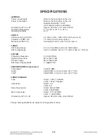
Page 23: ...2 8 A60 3 SPEAKER SECTION FRONT SPEAKER ...

Page 24: ...Figure 2 1 Case Top 1 1 Remove the 7 Screws 1 2 Remove the Case Top 2 Panel Front Assembly 2 1 Disconnect the 4 FFC Cables from the Main Board 2 2 Unhook the 10 Locking Tabs by using Flat head screwdriver 2 3 Remove the Panel Front Assembly ...

Page 25: ...1 1 Insert a Flat head screwdriver in the hole H1 3 1 2 Remove the Multi Knob 3 2 Jack PCB 3 2 1 Remove the 2 Screws 3 2 2 Remove the Jack PCB 3 3 BT Module 3 3 1 Unhook the Locking tab L1 3 3 2 Remove the BT Module 3 4 Front PCB 3 4 1 Remove the 11 Screws 3 4 2 Remove the Front PCB ...

Page 26: ...2 11 Figure 4 4 Bracket Hook 4 1 Remove the 2 Screws 4 2 Rotate 90 degrees to the front 4 3 Remove the Bracket Hook ...

Page 27: ...e 5 5 Main PCB SMPS PCB 5 1 Remove the 2 Screws from the Panel Rear 5 2 Disconnect the 4 FFC Cables from the Main Board 5 3 Remove the 10 Screws from the Main Board SMPS Board 5 4 Remove the Main Board SMPS Board ...

Page 28: ...2 13 Figure 6 6 Bracket Inner 6 1 Remove the 2 Screws from the Panel Rear 6 2 Remove the 2 Screws from the Bracket Inner 6 3 Remove the Bracket Inner ...

Page 29: ...anel Rear 8 1 Remove the 1 Screw from the Panel Rear 8 2 Remove the Panel Rear Figure 7 7 MD Lighting PCB 7 1 Remove the 2 Screws from the MD 7 2 Remove the 2 Screws from the Lighting PCB 7 3 Remove the MD Lighting PCB ...

Page 30: ...DISPLAYED WHEN POWER ON THE SET 3 24 ELECTRICAL TROUBLESHOOTING GUIDE 3 25 1 POWER SUPPLY ON SMPS BOARD 3 25 2 SYSTEM PART 3 28 3 NO AUDIO CHECK 3 29 WAVEFORMS OF MAJOR CHECK POINT 3 34 1 DSP IC501 3 34 2 PWM IC600 3 35 3 SERVO IC401 3 36 4 MOTOR DRIVER IC400 3 37 5 ADC 3 38 6 USB 3 38 7 BLUETOOTH 3 39 WIRING DIAGRAM 3 41 BLOCK DIAGRAM 3 43 CIRCUIT VOLTAGE CHART 3 45 1 CAPACITOR VOLTAGE 3 45 PRINT...

Page 31: ...ountermeasure 1 Check if the fuse F901 is open or short circuit 2 Check if the bridge diode BD901 is short circuit by over current with a digital multi meter 3 Check if the NTC thermistor TH900 TH903 is normal or open 1 1 3 Service hint Any picture Remark F901 If F901 is not short circuit replace it with a same specifications one BD901 If BD901 is short circuit replace it with a new one TH900 TH90...

Page 32: ...eck if the fuse F911 is open or short circuit 2 Check the Drain Source or Drain Gate Gate Source Resistance of Q905 Q906 with a digital multimeter If it is short condition it s destroyed Replace it with a new one Please replace 2 FET at the same time although several FET is OK 1 2 3 Service hint Any picture Remark F911 If F911 is not short circuit replace it with a same specifications one Q905 Q90...

Page 33: ...re is no 5 6 VA check the SMPS and if doesn t appear 3 3 V check IC306 2 Check 5 6 VA 12 V F F an VH when power on the set If the set doesn t work regardless of what the KEY1 changes high to low while pressing the power button X500 and X501 work normally but if you can not power on the set replace the IC501 with a new one on the main board 2 1 3 Service hint Any picture Remark MAIN board top view ...

Page 34: ...C301 pin4 on MAIN board If IC306 pin5 about 3 4 V doesn t come out check 3 4 VA from IC301 If IC301 pin4 about 4 9 V doesn t come out check 5 1 VA from SMPS 2 If IC306 pin3 about 3 4 V is normal check the PWR_CTRL IC306 pin4 is high about 3 3 V If PWR_CTRL isn t high check pin D11 of IC501 R550 3 If PWR_CTRL is high check R550 and if there s no defective component then replace IC306 4 If 3 3 V VCC...

Page 35: ... 3 2 2 How to troubleshoot Countermeasure 1 If 3 3 V 1 2 V is normal check reset HIGH of IC501 pin T12 on MAIN board If MAIN_RESET isn t HIGH check MICOM IC100 pin40 2 If MAIN_RESET is HIGH check the soldering status of 24 MHz crystal X500 3 If the crystal X500 doesn t oscillate check R551 R55E C536 C53B around crystal X500 If there s no defective component then replace X500 3 2 3 Service hint Any...

Page 36: ...How to troubleshoot Countermeasure 1 If the crystal X500 does oscillate check Serial Flash IC503 on MAIN board Check pin8 VCC pin6 CLK pin1 CS pin2 DO pin5 DI of below waveform 2 If pin1 2 5 6 8 doesn t come out check damping resistor R54A R54B R54C R54D of IC503 If damping resistor of IC503 is OK then replace IC503 it need to download program 3 After change IC503 if It is still not below waveform...

Page 37: ... on MAIN board 3 4 2 How to troubleshoot Countermeasure 1 Check below waveform soldering status of SDRAM IC504 on MAIN board If pin17 CAS pin18 RAS pin19 CS pin38 CLK pin29 address pin2 DQ doesn t come out check damping resistor R565 R567 R569 R563 2 If resistor is OK then replace IC502 SDRAM 3 After change IC504 if It is still not below waveform check IC501 DSP IC 3 4 3 Service hint Any picture R...

Page 38: ...SP IC501 3 5 1 Solution Please check and replace IC501 on MAIN board 3 5 2 How to troubleshoot Countermeasure 1 After check them by previous pages about no booting if the set is still no booting Check soldering status of IC501 2 If below bootstrap waveform doesn t come out then replace IC501 DSP IC 3 5 3 Service hint Any picture Remark R578 PGPB07 YELLOW R598 PAD19 GREEN R597 PAD20 PINK Bootstrap ...

Page 39: ... pin16 of IC401 If no signal check 3 3 V RF and X400 2 Check the SP SP from IC400 to CN401 for driving SPINDLE motor It is about 3 6 Vp p If no signal check 1 8 V and DVCC 5 V for IC400 3 Check if the FFC cable is solidly connected between CN401 and MD 4 Check the MD If the spindle motor is short circuit or has any trouble it can not rotate CD discs Please check the function after changing another...

Page 40: ...IC400 on MAIN board 4 2 2 How to troubleshoot Countermeasure 1 Check the SLDO signal from pin23 of IC401 If no signal check 3 3 V RF and X400 2 Check the SLED SLED from IC400 to CN401 for driving SPINDLE motor It is about 2 9 Vp p If no signal check 1 8 V and 5 V for IC400 3 Check if the FFC cable is solidly connected between CN401 and MD 4 Check the MD If the sled motor is sort circuit or has any...

Page 41: ...OAD from IC400 to CN401 for driving the tray open close motor It is about 3 85 Vp p If no signal check 5 V to IC401 If it has any trouble replace it with a new one 3 Check if the FFC cable is solidly connected between CN401 and MD 4 Check the MD If the tray motor is short circuit or has any trouble it can not open or close the tray Please check the function after changing another MD 4 3 3 Service ...

Page 42: ...a track on CD disc 1 Check the TRD signal from pin14 of IC401 If no signal check 3 3 V RF and X400 2 Check TR TR from IC400 to CN400 for driving the tracking actuator If no signal check 1 8 V and 5 V for IC400 3 Check if the FFC cable is solidly connected between CN400 and MD 4 Check the MD If the pickup module has any trouble it can not move the laser beam on the left or right side Please check t...

Page 43: ...he surface of a CD disc 1 Check the FDO signal from pin21 of IC401 If no signal check 3 3 V RF and X400 2 Check F F from IC400 to CN400 for driving the focusing actuator If no signal check 1 8 V and 5 V for IC400 3 Check if the FFC cable is solidly connected between CN400 and MD 4 Check the MD If the pick up module has any trouble it can not move the laser beam on the top or bottom side Please che...

Page 44: ...r IC303 on MAIN board 5 1 2 How to troubleshoot Countermeasure 1 Check USB_5V to MAIN board if 5 1 VA to pin5 of IC303 LDO doesn t come out check pin4 pin5 of CN503 if 5 1 VA is normal USB_5V of IC303 pin1 doesn t come out then replace IC303 2 Check Digital audio AMP block 5 1 3 Service hint Any picture Remark D D D D USB D D CN503 pin4 pin5 Waveform of USB D signal MAIN board top view CN503 CN503...

Page 45: ...this system is on bass blast mode C RL and RR make sound only on bass blast mode 2 Check the IC700 IC702 IC800 IC802 on your eyes 3 Check the audio signal output check pin13 of IC700 IC702 IC800 IC802 First check the PWM data input pin3 of IC700 IC702 IC800 IC802 4 If the audio signal output has no output try to change IC which has no output 5 Lastly check speaker terminal JK700 6 1 3 Service hint...

Page 46: ...urs when DC protection is detected MAIN reasons are like below When some of AMP FETs dead 7 1 3 Service hint Any picture Remark Notice for FET service In case of RF6775 Metal case FET Drain has electric potential So be careful when you deal with it You can see FET after removing heatsink Notice for Service Before repair MAIN Assy you need to discharge SMPS After then open the connector You should ...

Page 47: ...gnal Normal supply voltage and signal Check AMP IC Poor supply voltage Check SMPS assy Poor signal Check PWM IC 2 Check CSD of FET driver IC IRS2092 EAN60778301 CSD has about 5 V on normal state When AMP has problem CSD is LOW state or keep change LOW to HIGH 8 1 3 Service hint Any picture Remark MAIN board top view AMP IC AMP IC CN800 CN800 pin1 2 66 V pin1 2 66 V pin3 4 PGND pin3 4 PGND pin5 6 6...

Page 48: ... If is NG replace it a new one 4 Check the following I2S signal flow from IC501 to IC600 If there is any trouble check the power for each IC The power is normal but if the signal waveform to the IC is distorted or no signal replace it with a new one 5 Check if the digital audio AMP block is okay If AMP is damaged replace it with a new one 9 1 3 Service hint Any picture Remark MAIN board top view A...

Page 49: ...heck if ADC_BCK ADC_LRCK DAC_MCLK are entered from IC501 to IC201 5 Check if ADC_DATA is entered from IC201 to IC501 If no signal check 5 V 3 3 V ADC for IC201 If is NG replace it a new one 6 Check the following I2S signal flow from IC501 to IC202 If there is any trouble check the power for each IC The power is normal but if the signal waveform to the IC is distorted or no signal replace it with a...

Page 50: ...e entered from IC501 to IC200 3 Check if ADC_DATA is entered from IC200 to IC501 If no signal check 3 3 V ADC for IC200 If is NG replace it a new one 4 Check the following I2S audio signal flow from IC501 to IC600 If there is any trouble check the power for each IC The power is normal but if the signal waveform to the IC is distorted or no signal replace it with a new one 5 Check if the digital au...

Page 51: ...e if it has a problem 4 Check if MCS_BCK MCS_LRCK MCS_MCLK are entered from IC501 to IC200 5 Check if ADC_DATA is entered from IC200 to IC501 If no signal check 3 3 V ADC for IC200 If is NG replace it a new one 6 Check the following I2S signal flow from IC501 to IC600 If there is any trouble check the power for each IC The power is normal but if the signal waveform to the IC is distorted or no sig...

Page 52: ... L1 to IC501 DSP 3 Check if MCS_BCK MCS_LRCK MIX_DATAN is entered from IC501 to IC202 If no signal check VCC12 1 2 V for IC501 If it is abnormal change replace it a new one 4 Check the following I2S signal flow from IC501 to IC202 If there is any trouble check the power for each IC If the signals are abnormal replace it a new one 5 Check if the digital audio AMP block is okay If AMP is damaged rep...

Page 53: ...10 1 2 How to troubleshoot Countermeasure 1 Check if VH F and F DVCC_3 3V are output from SMPS to VFD via the MAIN board 2 Check if the IC501 outputs VFD_CLK VFD_STB and VFD_DO to the FRONT board 3 Check if the VH FRONT_12V SW on the FRONT board If the VH from VFD DGND VDD isn t output replace VFD with a new one 10 1 3 Service hint Any picture Remark FRONT circuit FRONT circuit VFD_STB VFD_STB VFD...

Page 54: ...901 same fuse Check or replace D963 Is D960 D961 normal Replace BD901 Check P_CTL from μ com Check IC951 and replace Or check line of MAIN PCB is short or not Check or replace D960 D961 NO NO NO NO NO Is the F901 normal Is the VCC 12 VA supplied to IC951 pin1 Is the VCC 11 V 25 V supplied to IC901 pin4 Is BD901 normal Is there HIGH signal at IC951 pin4 ...

Page 55: ...replace Q951 Is the VCC 7 VA supplied to IC953 pin2 Is there H signal at Q953 Base NO NO NO Is the D959 normal YES YES YES No output AMP gate line Check or replace R952 Check or replace D952 D959 Check and replace IC952 Or check line of MAIN PCB is short or not Is the VCC 13 VA supplied to IC952 pin1 to pin3 NO NO Is the R952 normal YES YES POWER SUPPLY ON SMPS BOARD ...

Page 56: ...eplace IC902 and check Q905 Q906 gate pin1 Components Resistors Diodes Is Q905 Q906 OK Replace Q905 Q906 Check or replace D954 D955 Check line of MAIN PCB is short or not Is the C904 voltage about 390 V Is F911 normal Is the PFC P CTL OK Is the AMP P CTL OK Is the VCC 12 V supplied to IC904 pin16 Is the VCC 12 V supplied to IC902 pin2 NO YES NO NO NO NO YES NO YES YES YES YES NO NO POWER SUPPLY ON...

Page 57: ...ble Check MAIN board Check SMPS board Replace VFD301 F VH voltage OK Check MAIN board HELLO Display on FLD OK When turn the volume count is change NO NO NO NO NO NO NO CN101 cable connection OK Check CN101 pin3 4 I2C data OK CN101 pin5 6 7 data signal OK CN101 pin11 22 25 power OK YES YES YES YES YES YES ...

Page 58: ... Check loading motor Check IC501 OPU driving Focusing Tracking OK Check OPU Pick up module Is motor impedance about 12 Ω IC401 pin34 36 I2S output signal OK Can disc insert IC501 pin N1 N2 N4 I2S input signal OK Disc reading OK NO NO NO NO NO NO NO NO NO IC401 RF Servo signal OK Focusing Tracking Sled signal OK LOAD OK YES YES YES YES YES NO YES YES YES A 3 NO AUDIO CHECK ...

Page 59: ...wer USB_5 V OK YES A A When insert USB IC501 pin U7 U8 A7 A8 USB_D signal OK NO YES YES YES YES AUX Check audio cable Replace IC200 Check IC501 NO NO NO IC200 pin 3 4 AUX input signal OK IC200 pin18 ADC_data output signal OK IC200 pin15 16 17 I2S input signal OK NO AUDIO CHECK ...

Page 60: ...input signal OK IC200 pin18 ADC_data output signal OK IC200 pin15 16 17 I2S input signal OK TUNER Check IC501 Replace IC200 Check 3 3 V of TUN200 IC200 pin15 17 I2S input signal OK IC200 pin18 ADC data output signal OK NO NO NO TUN200 TUNER_L R output signal OK YES A IC200 pin1 2 TUNER_L R input signal OK NO YES YES YES NO AUDIO CHECK ...

Page 61: ...RICAL TROUBLESHOOTING GUIDE B A YES YES YES YES Check IC501 Replace IC600 Check IC501 NO NO NO IC501 pin D1 D2 E1 I2S Clock signal OK IC600 PWM data output signal OK IC501 pin E2 I2S data signal OK NO AUDIO CHECK ...

Page 62: ...Check Q706 Q707 Pin39 50 of IC600 FL FR signal OK Pin13 of IC700 IC801 FL FR audio signal OK IC601 IC603 FL FR audio signal OK 66 V 12 V 5 V power voltage OK Q700 Q701 Q802 Q803 OK Pin45 46 of IC600 SW1 signal OK Pin13 of IC702 SW1 audio signal OK IC602 SW1 audio signal OK 66 V 12 V 5 V power voltage OK Q706 Q707 OK NO NO NO NO NO NO NO NO NO NO YES YES YES YES YES YES YES YES YES YES OK NO AUDIO ...

Page 63: ...WAVEFORMS OF MAJOR CHECK POINT 1 DSP IC501 X XI XO X XI XO Fig 1 2 Crystal of system 24 MHz MAIN DSP R551 C53B X500 Fig 1 1 Crystal of RTC 32 768 MHz Both ends of R561 X501 This model is not used 2 1 3 4 4 3 ...

Page 64: ...3 35 2 PWM IC600 X XI XO Fig 2 2 DSP to PWM I2S IC600 pin26 pin30 Fig 2 1 Crystal 24 576 MHz IC600 pin4 pin5 X600 6 5 7 8 9 5 8 7 9 6 ...

Page 65: ...3 36 3 SERVO IC401 X XI XO Fig 3 2 CD 16M IC401 pin31 Fig 3 1 Crystal 16 9344 MHz X400 11 10 12 10 11 12 ...

Page 66: ...O LO MOT_OPEN MOT_CLOSE for Driving TRAY Motor IC400 pin6 pin7 pin9 pin10 16 15 14 13 Fig 4 3 SP SP for Driving SPINDLE Motor IC400 pin17 pin18 20 19 Fig 4 2 SL SL for Driving SPINDLE Motor IC400 pin11 pin12 18 17 17 18 19 20 13 15 14 16 ...

Page 67: ...3 38 5 ADC 6 USB Fig 6 USB D D CN503 pin4 pin5 pin7 pin8 Fig 5 ADC I2S IC200 pin16 pin17 pin18 23 21 22 24 25 25 24 23 22 21 ...

Page 68: ...3 39 7 BLUETOOTH B BT_TX BT_RX BT_RST BT_TX BT_RX BT_RST BT_TX BT_RX BT_RST Fig 7 BT_TX BT_RX BT_RST 28 26 27 28 27 26 ...

Page 69: ...3 40 ...

Page 70: ... MICOM IC200 ADC IC503 F S 16M IC504 SDRAM IC400 Motor DR Tuner MIC 2 MIC 1 PTB USB1 USB2 MAIN BT module AUX In MD SMPS Harness FFC FL RL FR RR W1 W2 Party Thruster JACK 4P FRONT 6P 12P 12P 6P 12P 12P 8P 25P 10P 8P 25P 10P 23P 10P 23P WIRING DIAGRAM ...

Page 71: ...T_P N RR_OUT_P N FR_OUT_P N M00_15 A00_16 SF_DI DO SF_CS SCK VFD_STB CLK DO RST MAIN VOL_A B KEY 1 2 3 OP_SW CL_SW UP_SW DN_SW D_SENSE MOT_MUTE CLOSE OPEN A B C D E F PD LD SPDO SLDO FOD TRD LOAD SLED SPIN TR F D2S IR_IN_FL IR_IN_SW1 IR_IN_RR IR_IN_FR PWM_DAT CLK RST DAT CD_RW MCLK LRCK BCK CD_DAT CD_RST UART_RX TX IC101 MICOM SCRATCH A B TOP_LED FRONT_AGL MID_AGL WOOFER_AGL MIC_DET PTB_DET SEARCH...

Page 72: ...9 11 89 C963 3300 uF 25 V 16 3 16 3 C964 220 uF 25 V 12 03 12 1 C966 1000 uF 80 V 67 66 9 C968 1000 uF 80 V 66 66 MAIN FRONT Board C318 47 uF 16 V 3 3 C328 47 uF 16 V 6 6 C334 1 uF 50 V 31 31 C335 1 uF 50 V 18 18 C336 1 uF 50 V 21 21 C337 1 uF 50 V 18 18 C402 100 uF 16 V 5 5 C404 47 uF 16 V 3 3 3 3 C409 47 uF 16 V 3 3 3 3 C416 47 uF 16 V 1 7 1 7 C418 3 3 uF 50 V 1 7 1 7 C427 220 uF 16 V 5 1 5 1 C6...

Page 73: ...3 47 3 48 PRINTED CIRCUIT BOARD DIAGRAMS 1 SMPS P C BOARD DIAGRAM TOP VIEW ...

Page 74: ...3 49 3 50 SMPS P C BOARD DIAGRAM BOTTOM VIEW NOTE Warning Parts that are critical with respect to risk of fire or electrical shock ...

Page 75: ...3 51 3 52 2 MAIN P C BOARD DIAGRAM TOP VIEW ...

Page 76: ...3 53 3 54 MAIN P C BOARD DIAGRAM BOTTOM VIEW ...

Page 77: ...3 55 3 56 3 FRONT P C BOARD DIAGRAM TOP VIEW ...

Page 78: ...3 57 3 58 FRONT P C BOARD DIAGRAM BOTTOM VIEW ...

Page 79: ...3 59 3 60 4 JACK P C BOARD DIAGRAM TOP VIEW BOTTOM VIEW ...

Page 80: ...Magnet 4 2 2 3 Clamp 4 2 3 Tray Disc 4 3 4 Pick Up Assembly 4 4 5 Base Up Down 4 4 6 Belt Loading 4 5 7 Gear Pulley 4 5 8 Gear Loading 4 5 9 Guide 4 5 10 Deck PCB Assembly 4 5 11 Motor Assembly 4 5 12 FFC Cable 4 5 DECK MECHANISM EXPLODED VIEW DM14B 4 6 SECTION 4 MECHANISM DM14B CONTENTS ...

Page 81: ...amp Assembly as Figure B 2 Bending the Cover Top in direction of arrow 2 as Figure B 3 Separate the Clamp Assembly from the Cover Top 2 1 Plate 1 Turn the Plate to a counterclockwise direction and then lift up the Plate 2 Remove the Plate 2 2 Magnet Remove the Magnet 2 3 Clamp Remove the Clamp 1 3 S1 L1 Cover Top Figure A 2 1 2 Figure B Clamp Assembly Clamp Assembly Plate Magnet Clamp ...

Page 82: ...Note When reassembling place the Guide as Figure E MD Sub Assembly Figure D 3 1 1 2 2 Tray Disc Tray Disc Figure E Guide 3 Tray Disc 1 Insert and push a flat head screwdriver in the Emergency eject hole H1 at the right side so that the Tray Disc is ejected about 15 20 mm 2 Pull the Tray Disc until it is locked Bottom side view Tray Disc Tray Disc Figure C 2 1 H1 Emergency eject hole ...

Page 83: ...reassembling insert the D portion of the Base Up Down in the Hole H2 of the Base Main as Figure G 3 3 2 1 L2 Base Up Down Figure G 2 Figure G 1 C B Guide Base Up Down Base Main Figure G B H2 A Figure G 3 D 4 Pick Up Assembly 1 Detach the Gasket Tape 2 Disconnect the wires BLK RED BRN ORN from the Deck PCB Assembly by desoldering 3 Remove the 4 screws S2 4 Disconnect the FFC Cable from the Pick Up ...

Page 84: ...CB Assembly 1 Disconnect the wires RED BK form the Deck PCB Assembly by desoldering 2 Remove the 1 screw S3 3 Separate the Deck PCB Assembly from the Base Main 11 Motor Assembly Unlock the Locking Tab L4 in direction of arrow and then separate the Motor Assembly from the Base Main 12 FFC Cable Remove the FFC Cable Gear Pulley Belt Loading Deck PCB Assembly Motor Assembly Base Main Gear Loading Gui...

Page 85: ...4 6 DECK MECHANISM EXPLODED VIEW DM14B 1439 A001 1002 1005 1001 1049 1437 1437 1024 1024 1024 1024 1003 1011 1437 1004 1026 1043 1045 A005 A006 1016 1013 1015 1020 1439 1018 1019 1012 1030 ...

Reviews: