background image

COLOR MONITOR

SERVICE MANUAL

Website:http://biz.LGservice.com

E-mail:http://www.LGEservice.com/techsup.html

CAUTION

BEFORE SERVICING THE UNIT, 
READ THE  SAFETY PRECAUTIONS IN THIS MANUAL.

CHASSIS NO. : LM57B

MODEL:

L1752TX (L1752TX-SFQ.AX**QP, AW**QP)
L1752TX (L1752TX-BFQ.AX**QP, AW**QP)
L1952TX (L1952TX-SFQ.AX**QP, AW**QP)
L1952TX (L1952TX-BFQ.AX**QP, AW**QP)

*To apply the MSTAR Chip.

(      ) **Same model for Service

Summary of Contents for AW**QP

Page 1: ...om techsup html CAUTION BEFORE SERVICING THE UNIT READ THE SAFETY PRECAUTIONS IN THIS MANUAL CHASSIS NO LM57B MODEL L1752TX L1752TX SFQ AX QP AW QP L1752TX L1752TX BFQ AX QP AW QP L1952TX L1952TX SFQ AX QP AW QP L1952TX L1952TX BFQ AX QP AW QP To apply the MSTAR Chip Same model for Service ...

Page 2: ...Hz 4 Max Resolution D sub Analog 1280 x 1024 75Hz Digital 1280 x 1024 60Hz 5 POWER SUPPLY 5 1 Power AC 100 240V 50 60Hz 0 8A 5 2 Power Consumption 6 ENVIRONMENT 6 1 Operating Temperature 10 C 35 C 50 F 95 F Ambient 6 2 Relative Humidity 10 80 Non condensing 6 3 MTBF 50 000 HRS with 90 Confidence Lamp Life 50 000 Hours Min 7 DIMENSIONS with TILT SWIVEL L1752TX Width 364 5 mm 14 35 Depth 180 mm 7 09...

Page 3: ... Protect the module from the ESD as it may damage the electronic circuit C MOS Make certain that treatment person s body are grounded through wrist band Do not leave the module in high temperature and in areas of high humidity for a long time The module not be exposed to the direct sunlight Avoid contact with water as it may a short circuit within the module If the surface of panel become dirty pl...

Page 4: ...st receiver ground lead to the receiver chassis ground before connecting the test receiver positive lead Always remove the test receiver ground lead last 9 Use with this receiver only the test fixtures specified in this service manual CAUTION Do not connect the test fixture ground strap to any heat sink in this receiver Electrostatically Sensitive ES Devices Some semiconductor solid state devices ...

Page 5: ...tip as the solder melts 2 Draw away the melted solder with an anti static suction type solder removal device or with solder braid before removing the IC Replacement 1 Carefully insert the replacement IC in the circuit board 2 Carefully bend each IC lead against the circuit foil pad and solder it 3 Clean the soldered areas with a small wire bristle brush It is not necessary to reapply acrylic coati...

Page 6: ...onnection 4 Route the jumper wire along the path of the out away copper pattern and let it overlap the previously scraped end of the good copper pattern Solder the overlapped area and clip off any excess jumper wire At Other Connections Use the following technique to repair the defective copper pattern at connections other than IC Pins This technique involves the installation of a jumper wire on t...

Page 7: ...ls 57 283 49 725 1152 832 32 64 224 832 x 624 V Lines 74 55 667 624 1 3 39 8 H Pixels 65 0 48 363 1344 1024 24 136 160 1024 x 768 V Lines 60 0 806 768 3 6 29 9 H Pixels 78 75 60 123 1312 1024 16 96 176 1024 x 768 V Lines 75 029 800 768 1 3 28 10 H Pixels 100 0 68 681 1456 1152 32 128 144 1152 x 870 V Lines 75 062 915 870 3 3 39 11 H Pixels 92 978 61 805 1504 1152 18 134 200 1152 x 900 V Lines 65 9...

Page 8: ... DISASSEMBLY Set Disassembly Like a picture Remove the screws 1 Pull the front cover upward 2 Then let the all latches are separated 3 1 3 2 3 Put the front face down Disassemble back cover 1 2 3 2 3 1 4 ...

Page 9: ... to Right side 2 Pull Stand and Separate Stand from Monitor set 3 Push the four latches on the bottom to the outside and Separate Stand Body Base Reference the 3 2 After finished repair necessarily push 4ea Latches to inside for restoration 1 2 3 1 3 2 3 3 4 ...

Page 10: ...arACE LVDS Tx LVDS Analog R G B Digital D Sub DVI D LIPS Filter 5V 12V 5V 3 3V 1 8V Vcc 5V 5V Scaler MCU Intel8032 Inverter 4 lamps 12V Regulator KEY 3 3V 1 8V Line Buffer OSD SSC EEPROM System Module 3 3V SDA SCL 3 3V Flash ROM 12V EEPROM EDID ...

Page 11: ...trol IC P ch N ch Inverter Trans SMPS Lamp Current Feedback Over Voltage Protection Power Control IC Feedback Line Filter L N Drive Block 12V 13V 5V Inverter On OFF 3 3V Dimming Lamp Current Control Aux Drive Start Module Vcc Main Board Scaler DC DC converter 12V 5V ...

Page 12: ...n signal and outputs 8 bit R G B signal to transmitter 2 Power Part This part consists of the one 3 3V and one 1 8V regulators to convert power which is provided 5V in Power board 12V is provided for inverter 5V is provided for LCD panel Also 5V is converted 3 3V and 1 8V by regulator Converted power is provided for IC in the main board The inverter converts from DC12V to AC 700Vrms and operates b...

Page 13: ...DC voltage through a bridge rectifier and a bulk capacitor 3 Energy Transfer This part function is for transfer the primary energy to secondary through a power transformer 4 Output rectifier and filter This part function is to make a pulse width modulation control and to provide the driver signal to power switch to adjust the duty cycle during different AC input and output loading condition to ach...

Page 14: ... is available to LCD Monitor only 1 Port Setup a Copy UserPort sys file to c WINNT system32 drivers folder b Run Userport exe c Remove all default number d Add 300 3FF e Click Start button f Click Exit button 2 EDID Read Write 1 Run WinEDID exe 2 Edit Week of Manufacture Year of Manufacture Serial Number a Input User Info Data b Click Update button c Click Write button ...

Page 15: ...display 2 Wait for about 5 seconds and press MENU POWER switch with 1 second interval 3 The SVC OSD menu contains additional menus that the User OSD menu as described below a Auto Color W B balance and Automatically sets the gain and offset value b NVRAM INIT EEPROM initialize 24C08 c CLEAR ETI To initialize using time d AGING Select Aging mode on off e R G B 9300K Allows you to set the R G B 9300...

Page 16: ...RT POINT AS OPENING EACH POWER LINE NO PROBLEM 1 Waveforms U201 96 CHECK KEY CONTROL CONNECTOR ROUTINE CHECK U201 NO NO CHECK 3 3V LINE OPEN CHECK CHECK 3 3V LINE NO CHECK X TAL YES CHECK J403 VOLTAGE PIN5 PIN6 5V CHECK U301 PIN2 VOLTAGE 3 3V IS U201 PIN75 3 3V VOLTAGE CHECK U201 PIN 96 PULSE 1 YES YES YES ...

Page 17: ...OARD AND FIND OUT A SHORT POINT AS OPENING EACH POWER LINE CHECK MICOM INV ON OFF PORT 1 CONFIRM BRIGHTNESS OSD CONTRL STATE 2 CHECK MICOM DIM ADJ PORT LIPS J403 PIN5 PIN6 5V J403 PIN9 5V J403 PIN10 5V CHECK PULSE AS CONTACTING SCOPE PROBE TO CAUTION LABEL CONTACT PROBE TO CAUTION LABEL CAN YOU SEE PULSE AT YOUR SCOPE YES YES YES YES ...

Page 18: ...CHECK C210 C211 SOLDERING CONDITION 2 CHECK X201 3 TROUBLE IN U201 CHECK CONNECTION LINE FROM D SUB TO U201 U201 PIN96 97 OSCILLATE AS 14 31MHZ U201 PIN27 IS 48KHz H SYNC PIN28 IS 60Hz V SYNC IS PULSE APPEARED AT SIGNAL PINS AT MODE 12 1 2 1 2 Waveforms U201 96 97 U201 27 H SYNC 2 U201 28 V SYNC YES YES YES U201 PIN 16 75 3 3V ...

Page 19: ...ROUBLE IN DPM TROUBLE IN DPM NO NO TROUBLE IN U201 CHECK PC PC IS NOT GOING INTO DPM OFF MODE CHECK H V SYNC LINE CHECK R442 R443 CHECK U201 PIN 27 28 SYNC PULSE 3 3 Waveforms R442 H Sync 3 R443 V Sync YES YES ...

Page 20: ...Line NO NO Check BD101 Check U101 Pin7 9 10V Check D102 Trouble in Q101 NO Trouble in D201 D202 YES CHECK Fuse F101 OK CHECK C101 Voltage AC110V 160Vdc AC220V 304Vdc CHECK U101 Pin6 Waveform Square wave Come out Check Q101 Drain Waveform Check D201 D202 Voltage YES YES YES YES NO ...

Page 21: ...k the waveform of U301 Pin11 12 19 20 Check the waveform of U301 Pin11 12 19 20 NO If waveform is no problem Check Q303 Q308 Or Trouble in U303 U304 YES CHECK P201 Pin9 3 3V Check U301 Pin3 5V Check U301 Pin2 OVP Less than 1 8V Check U301 Pin10 CMP Less than 2 75V Check U303 U304 Drain waveform YES YES YES NO ...

Page 22: ... 22 WIRING DIAGRAM 11P 6P 3P 30P 6631900011H 6631T20023J 6631900109A 6631T20010E L1752TX 6631900125A L1952TX ...

Page 23: ... 23 EXPLODED VIEW 010 020 100 110 120 130 030 200 160 170 190 180 090 080 140 150 040 050 070 060 ...

Page 24: ...ASSEMBLY LX52 35509K0241 STAND BASE ASSY 35509K0245A COVER L1752S STAND BODY 35509K0246A COVER L1952S STAND BODY 3520900038A INDICATOR LED PRE AMP LX52 PMMA NON LED LENS 49509K0266A METAL SHIELD LX52 LAMP L1752TX 49509K0267A METAL SHIELD L1952 LAMP 68719STA24C PWB PCB ASSEMBLY SUB SUB T T LM57A LX52 KXRDQPT NT CKD CONTROL L1752TX 68719STA24D PWB PCB ASSEMBLY SUB SUB T T LM57A L1919S KXRDQPT NT CKD...

Page 25: ...T006D C3216X7R1E225M TDK 25V 2 2UF DATE 2006 02 08 S AL LOC NO PART NO DESCRIPTION SPECIFICATION C306 0CE477EF638 470UF KMG 16V M FM5 TP 5 C306 0CK224DH56A 0 22UF 2012 25V 10 R TP X7R C307 0CH3104K566 0 1UF 50V 10 X7R 2012 R TP C308 0CK105DH56A 1UF 2012 25V 10 X7R R TP C309 0CK224DH56A 0 22UF 2012 25V 10 R TP X7R C310 0CK105DH56A 1UF 2012 25V 10 X7R R TP C313 0CH2393K516 39000PF 50V 10 B Y5P 2012 ...

Page 26: ... 0TR390609DC 2N3906S RTK KEC REEL TAPING Q305 0TFDI80001A 2N7002 DIODES R TP SOT23 60V Q306 0TFDI80001A 2N7002 DIODES R TP SOT23 60V Q307 0TR390609DC 2N3906S RTK KEC REEL TAPING Q308 0TRKE80046A 2N3904S KEC R TP SOT23 60V 2 Q401 0TR390609FA FAIRCHILD KST3906 MTF TP SOT Q402 0TR390609FA FAIRCHILD KST3906 MTF TP SOT U302 0TFVI80067A SI3865BDV E3 VISHAY R TP TS U303 0TFAN00001A AP4511GD ADVANCED POWE...

Page 27: ... 10 W 5 1608 R TP R441 0RJ0000D677 0 OHM 1 10 W 5 1608 R TP R442 0RJ0682D677 68 OHM 1 10 W 5 1608 R TP R443 0RJ0682D677 68 OHM 1 10 W 5 1608 R TP R444 0RJ0332D677 33 OHM 1 10 W 5 1608 R TP R445 0RJ0752D677 75 OHM 1 10 W 5 1608 R TP R446 0RJ0752D677 75 OHM 1 10 W 5 1608 R TP DATE 2006 02 08 S AL LOC NO PART NO DESCRIPTION SPECIFICATION R448 0RJ0752D677 75 OHM 1 10 W 5 1608 R TP R450 0RJ4701D677 4 7...

Page 28: ...470K OHM 1 4 W 5 3216 R TP R102 0RJ6801E472 6800 OHM 1 8 W 1 2012 R TP DATE 2006 02 08 S AL LOC NO PART NO DESCRIPTION SPECIFICATION R103 0RH1004D622 1M OHM 1 10 W 2012 5 00 D R104 0RH1001D622 1K OHM 1 10 W 2012 5 00 D R105 0RD0912Q609 91 OHM 1 4 W 3 4 5 TA52 R106 0RH2201D622 2 2K OHM 1 10 W 2012 5 00 R107 0RD8203A609 820K OHM 1 2 W 7 0 5 00 TA R108 0RD4702A609 47K OHM 1 2 W 7 0 5 00 TA5 R109 0RX0...

Page 29: ...ULK L P201 6602T20008K SMW200 11 YEONHO 11P 2 0MM L P401 6630V90218A 35001WR YEONHO 2P 3 5MM DIP P402 6630V90218A 35001WR YEONHO 2P 3 5MM DIP P403 6630V90218A 35001WR YEONHO 2P 3 5MM DIP P404 6630V90218A 35001WR YEONHO 2P 3 5MM DIP J30 971 0016 TIN HDC 0 60H NON NON J31 971 0016 TIN HDC 0 60H NON NON 29 ...

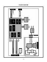
Page 30: ...SCHEMATIC DIAGRAM 30 1 SCALER ...

Page 31: ... 31 2 POWER WAFER ...

Page 32: ... 32 3 INVERTER ...

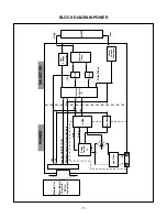
Page 33: ... 33 4 POWER ...

Page 34: ...Feb 2006 P NO 38289S0041 Printed in Korea ...

Reviews: