LG 32LG40 Series, Training Manual
The LG 32LG40 Series is a cutting-edge TV with impressive specifications. Delve into every detail and explore its features effortlessly with our comprehensive user manual, available for free download at manualshive.com. Get your hands on this manual now and unlock the full potential of your LG 32LG40 Series TV.
Share
Download


Reviews:
No comments
Related manuals for 32LG40 Series
TDC2015S
Brand: Haier Pages: 31
DTA-2198
Brand: Haier Pages: 29
SLC-1569A-3
Brand: Skyworth Pages: 37
13MC3206 - Tv/dvd Combination
Brand: Magnavox Pages: 2
20MDRF20
Brand: Magnavox Pages: 48
13MC3206 - Tv/dvd Combination
Brand: Magnavox Pages: 64

CFTD2085
Brand: Samsung Pages: 100
UW-17J11VD
Brand: Samsung Pages: 84
BeoCenter 1
Brand: Bang & Olufsen Pages: 24
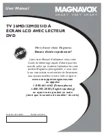
32MD251D - 32" Lcd Hd Flat Tv
Brand: Magnavox Pages: 46
19MD357B - Hook Up Guide
Brand: Magnavox Pages: 2

19MD350B
Brand: Magnavox Pages: 57
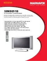
32MD251D - 32" Lcd Hd Flat Tv
Brand: Magnavox Pages: 2
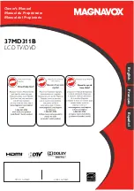
37MD311B
Brand: Magnavox Pages: 42
26MD350B -
Brand: Magnavox Pages: 56
13MDTD20 - Dvd-video Player
Brand: Magnavox Pages: 60
19MD357B - Hook Up Guide
Brand: Magnavox Pages: 3

13MDTD20 - Dvd-video Player
Brand: Magnavox Pages: 60


