background image

SERVICE MANUAL

COPYRIGHT © 2015 JVC KENWOOD Corporation

No.RA020<Rev.002>

2015/10

B5B-7172-10

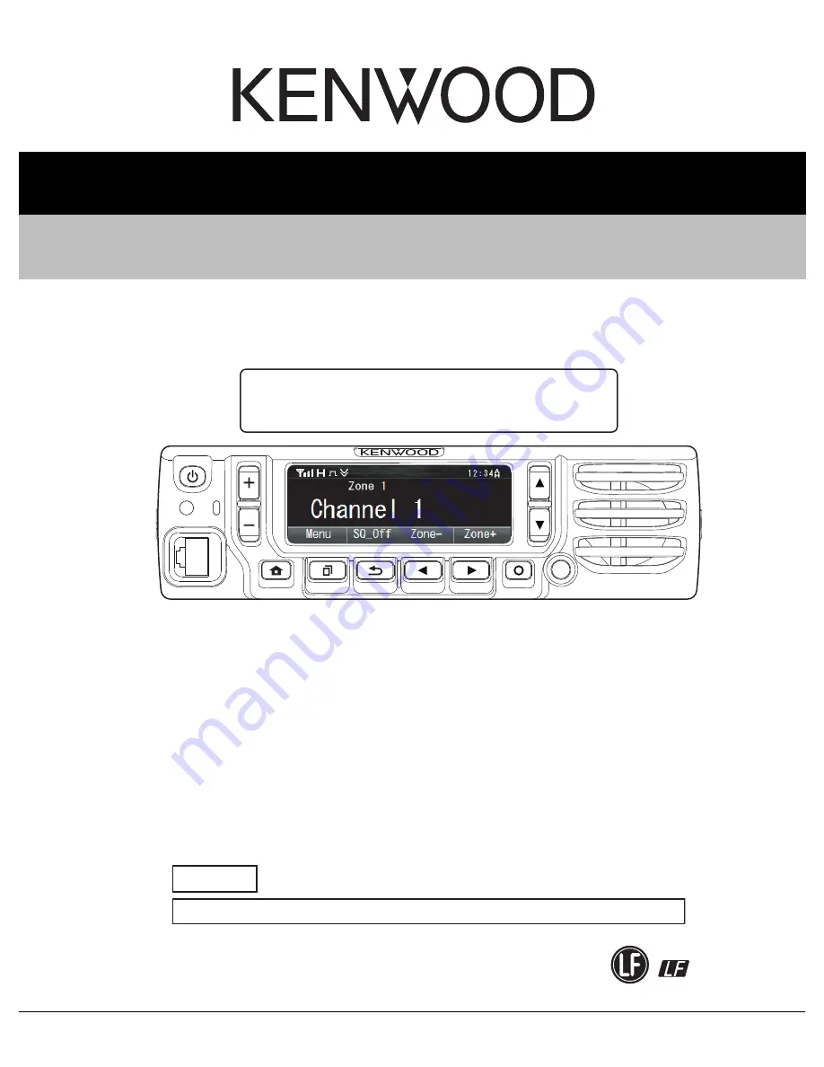
VHF DIGITAL TRANSCEIVER

RA020<Rev.002>

2015

10

SERVICE MANUAL

B5B-7172-10

NX-5700, NX-5700(B)

COPYRIGHT © 2015 JVC KENWOOD Corporation

TABLE OF CONTENTS

1

PRECAUTION. . . . . . . . . . . . . . . . . . . . . . . . . . . . . . . . . . . . . . . . . . . . . . . . . . . . . . . . . . . . . . . . . . . . . . . . .  1-4

2

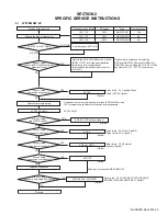
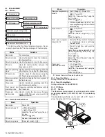
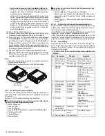
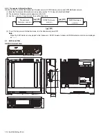
SPECIFIC SERVICE INSTRUCTIONS . . . . . . . . . . . . . . . . . . . . . . . . . . . . . . . . . . . . . . . . . . . . . . . . . . . . . .  1-5

3

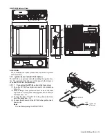
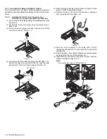
DISASSEMBLY  . . . . . . . . . . . . . . . . . . . . . . . . . . . . . . . . . . . . . . . . . . . . . . . . . . . . . . . . . . . . . . . . . . . . . .  1-32

4

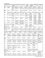
ADJUSTMENT . . . . . . . . . . . . . . . . . . . . . . . . . . . . . . . . . . . . . . . . . . . . . . . . . . . . . . . . . . . . . . . . . . . . . . .  1-36

5

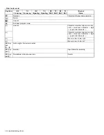
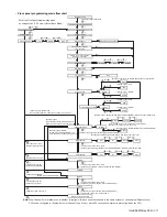
TROUBLESHOOTING . . . . . . . . . . . . . . . . . . . . . . . . . . . . . . . . . . . . . . . . . . . . . . . . . . . . . . . . . . . . . . . . .  1-94

NX-5700 is a model that operation panel is attached. 
NX-5700(B) is a model that operation panel is not attached. 
The illustration is NX-5700.

This service manual has been revised due to the addition of NX-5700 type E.

REVISED

This product complies with the 

RoHS

 directive for the European market.

This product uses Lead Free solder.

Summary of Contents for NX-5700

Page 1: ... 1 PRECAUTION 1 4 2 SPECIFIC SERVICE INSTRUCTIONS 1 5 3 DISASSEMBLY 1 32 4 ADJUSTMENT 1 36 5 TROUBLESHOOTING 1 94 NX 5700 is a model that operation panel is attached NX 5700 B is a model that operation panel is not attached The illustration is NX 5700 This service manual has been revised due to the addition of NX 5700 type E REVISED This product complies with the RoHS directive for the European ma...

Page 2: ...rohibited without prior written consent of JVC KENWOOD Corporation Furthermore any reselling assigning or transferring of the firmware is also strictly prohibited without embedding the firmware in KENWOOD product memories Transceivers containing AMBE 2 Vocoder The AMBE 2 voice coding technology is embedded in the firmware under the license of Digital Voice Systems Inc Bluetooth Copyrights The Blue...

Page 3: ...5 Operating Temperature Range 22 F to 140 F 30 C to 60 C Frequency Stability 1 0ppm Dimensions W x H x D Radio w Control Head 6 73 x 1 89 x 6 93 in 171 x 48 x 176 mm Weight net Radio w Control Head 3 53 lbs 1 6 kg RECEIVER Sensitivity NXDN 6 25kHz Digital 3 BER 0 20μV NXDN 12 5kHz Digital 3 BER 0 25μV P25 Digital 5 BER 0 25μV P25 Digital 1 BER 0 40μV Analog 12dB SINAD 0 25μV Selectivity P25 Digita...

Page 4: ...Antenna Impedance 50Ω Dimensions W x H x D Radio w Control Head 171 x 48 x 176 mm Weight net Radio w Control Head 1 6 kg RECEIVER Sensitivity Analogue 12 5 20 25 kHz 12dB SINAD 0 32 μV 0 28 μV 20dB SINAD 1 dB μV 0 45 μV 3 dB μV 0 35 μV Digital 6 25 12 5 KHz NXDN 3 BER 0 25 μV 0 32 μV NXDN 1 BER 4 dB μV 0 32 μV 1 dB μV 0 45 μV P25 5 BER 0 28 μV Selectivity P25 Digital 63dB Analogue 12 5 kHz 70dB An...

Page 5: ... 19 KCT 23 DC cable KCT 23 M M3 Are you using the secure cryptographic module NO Option YES KWD AE30 or KWD AE31 Refer to the 2 3 2 Horn Alert P A Relay Unit KAP 2 Option Refer to the 2 3 3 External Speaker Option Refer to the 2 3 1 Ignition Sense Cable KCT 46 Option Refer to the 2 3 4 SECURE CRYPTOGRAPHIC MODULE KWD AE30 KWD AE31 Option Head remote kit Are you using the GPS function KRA 40 GPS ac...

Page 6: ...er to another Front panel pro gramming mode Frequency signaling and features write to the transceiver Transceiver infor mation mode Used to confirm the transcerver firmware version SCM firmware version and SCM Hardware version Mode Operation User mode Power ON Panel test mode 2 Power ON Power ON Select the Panel Test using the key Press the key PC mode Received commands from PC Panel tuning mode P...

Page 7: ...ter the Firmware programming mode by using section 2 2 2 How to Enter Each Mode Then the yellow LED on the transceiver light and FIRMWARE PROG is displayed 5 Check the connection between the transceiver and the per sonal computer and make sure that the transceiver is in the Program mode 6 Press Write button in the window When the transceiver starts to receive data the LOADING display lights 7 If w...

Page 8: ...el Type Channel Spacing Decode QT DQT RAN NAC Encode QT DQT RAN NAC Talkgroup ID List No Transmit Power Channel Name Key guide on the Clone Front Panel Programming Pass word input screen Confirm key The password confirmation Delete key Delete the latest digit from the current password number Press and hold to delete all password numbers Select key Determine the latest digit of the password number ...

Page 9: ...IC Key pad Decision Decision Decision Decision Decision Decision Decision Decision MIC Key pad Unused Back to the previous item Back to the pre vious item Back to the previous item Back to the previous item Back to the previous item Back to the previous item Back to the previous item Key Item RX RAN TX RAN RX NAC TX NAC TG ID List No Transmit Power Channel Name Decision Decision Decision Decision ...

Page 10: ...nel program mode Unused Character selection upper case char acter lower case character digit upper case character Character selection upper case char acter lower case character digit upper case character Move a cursor to the right Move a cursor to the left MIC Key pad 0 9 Add a digit to the current number MIC Key pad Decision Input character switching MIC Key pad Delete Back to the previous item D...

Page 11: ...one Front Panel Password TX Frequency Other than OFF Channel Type P25 Mixed Transmit Mode P25 Talkgroup List ID Amount 0 Channel Type P25 Mixed Transmit Mode P25 Talkgroup ID List Amount must not be 0 RX RAN TX RAN NXDN TX Frequency OFF Channel Type P25 System Type P25 System Type NXDN 6 25Hz Channel Type NXDN Mixed Transmit Mode NXDN or No No Channel Type Analog Mixed Transmit Mode NXDN Mixed Tra...

Page 12: ...s 4 To exit the transceiver information mode turn the transceiver power OFF Note When the SCM board is not equipped to the transceiver SCM Firmware Version and SCM Hardware Version are displayed as 2 3 INSTALLATION NX 5700 External View 㪫㫉㪸㫅㫊㪺㪼㫀㫍㪼㫉㩷 㪽㫀㫉㫄㫎㪸㫉㪼㩷㫍㪼㫉㫊㫀㫆㫅 㪪㪚㪤㩷㪝㫀㫉㫄㫎㪸㫉㪼㩷 㫍㪼㫉㫊㫀㫆㫅 㪪㪚㪤㩷㪟㪸㫉㪻㫎㪸㫉㪼㩷 㫍㪼㫉㫊㫀㫆㫅 CAUTION AVOID CON TACT DURING PROLONGED USE HOT SUR FACE E S NO Made in Malaysia 01234567...

Page 13: ...ect the plug of the KCT 46 to the yellow cable termi nal of the transceiver 3 4 Connect the other end of the KCT 46 to the ignition line of the car 4 Note You must setup using the KPG D1 D1N Fig 1 148 5 171 151 48 170 M4 24 35 47 CAUTION AVOID CON TACT DURING PROLONGED USE HOT SUR FACE FCC RULES OPER ATION IS SUBJECT TO THE THIS DEVICE COMPLIES WITH PART 15 OF THE FOLLOWING TWO CONDITIONS 1 THIS D...

Page 14: ... wire with connector E37 1114 05 into the relay unit connector CN3 2 and the other side into the TX RX unit A 2 connector CN910 3 Fig 2 2 5 Place the relay unit at the position shown in Figure 2 2 and secure it to the chassis with a screw 6 Remove the cap on the rear of the chassis by pushing it from the inside with your finger 4 Fig 2 3 7 Pass the 6 pin connector of the cable E37 1113 25 through ...

Page 15: ...to pins 5 and 6 on the KAP 2 When you use the KES 5 plug the short pin to pins 5 and 6 on the KAP 2 When you use the INT SP or KES 3 plug the short pin to pins 4 and 5 on the KAP 2 Fig 3 2 Connection Procedure Insert the crimp terminal into the Square plug supplied with the KAP 2 Fig 3 3 KAP 2 Cable E37 1113 25 6 pin Connector KAP 2 CN1 Connect Set Up 4 5 INT SP or KES 3 5 6 KES 5 KAP 2 cable HR1 ...

Page 16: ...ther similar implement to remove the module you may inadvert ently damage the TX RX PCB and the module Cushion B cannot be reused Attach a new cushion B when you remove the cushion from the module 6 Reinstall the cabinet top packing and shielding plate of the transceiver Note When the KWD AE30 KWD AE31 is installed select the Secure Cryptographic Module checkbox in the Product Information of the P...

Page 17: ...emove the R950 chip jumpers and solder the chip jumpers to R952 2 3 5 2 Change configuration of D SUB 25 pin connector from DI to RTS 5 pin The input 5 pin of D SUB 25 pin connector is configured at the DI as the default value Remove the R943 chip jumpers and solder the chip jumpers to R946 Ref No Function R950 R952 Default AUXIO9 R950 R952 CTS RS 232C Ref No Function R943 R946 Default DI R943 R94...

Page 18: ...olithic crystal filter XF600 to reject adjacent channel signal The filtered first IF signal is amplified by the first IF amplifier Q604 and Q603 and then applied to the IF system IC IC600 The IF system IC provides a second mixer second PLL AGC and A D converter The second mixer mixes the first IF signal with the 47 7MHz of second local oscillator output and produces the second IF signal of 2 25MHz...

Page 19: ...er output in adjusted value by monitoring it with a coupler RF detection and comparison functions are included in the power control IC IC304 The power control IC output is given as a drive source of the RF power module s gate IC302 and completes APC feedback loop When an normal antenna load is connected reflected Forward RF Power is detected by the coupler and direct in power control IC IC304 Forw...

Page 20: ...rcuit consists of MPU DSP IC706 and its peripheral circuits IC706 mainly performs the following 1 Switching between transmission and reception by PTT signal input 2 Reading system zone frequency and program data from the memory circuit 3 Sending frequency program data to the PLL 4 Controlling the audio mute circuit by decode data input 2 4 6 1 MPU The MPU DSP IC706 is 32bit RISC processor and fixe...

Page 21: ...olled by PSW signal 54M goes to DC DC converter A1 IC11 AVR ICs IC5 IC4 IC12 IC14 IC7 IC10 IC6 and IC17 A1 12M is enabled while the 54M is operating 12M provides the power to the MPU DSP IC706 and turns on IC11 18M 18M provides the power to the MPU DSP and Mobile DDR IC702 and turns on IC5 33M IC14 33OPT 33M provides the power to the MPU DSP Flash memory IC701 and many control circuits and turns o...

Page 22: ... PLL IF VCO Assist Frontend Tuning 200C VCO Common Amp Fin Amp Fin filter switch VCO buffer Amp RX Heter SW Local Amp LNA 1st Mixer IF Amp 50R RXC 50BU SCTAM1 Option Board BINT Q8 Q9 D11 5V Reg TX RX VCO 50CS Ripple Filter SAVE Q112 DC SW 33SD microSD SD_EN TX Heter SW Q81 DC SW MPU DSP Core MPU DSP PLL F1 IC8 5 4V DC DC IC1 3 1V AVR BAT_CNT from Power management IC IC2 Q1 Q3 DC SW A1 1 2V DC DC I...

Page 23: ... saw filter L11 Frequency configuration for Bluetooth is following There are two LO modes 2X and Offset LO OSLO 2X where LO is 2 RF_FREQ e g when transmitting at 2441MHz it is at 4882MHz OSLO where LO is at 2 3 RF_FREQ e g when transmitting at 2441MHz it is at 1627 333MHz In RX the 2X is always used In GFSK TX if power is 10dBm then OSLO is used In EDR2 TX if power is 12dBm then OSLO is used In ED...

Page 24: ...C Logic control IC711 IC I O expander IC712 IC A D converter IC714 IC Analog SW IC715 IC D A converter IC719 IC D A converter IC720 IC Reset IC900 IC Logic control IC901 IC DC AMP 25REF VREF IC902 IC CODEC IC903 IC AF AMP IC904 IC Logic control IC905 IC Buffer AMP BER CK BER DT IC906 IC Level shift IC907 IC Analog SW IC908 IC Schmitt trigger IC909 IC RS 232C driver IC910 IC I O expander IC911 IC A...

Page 25: ...R SW D501 507 Variable capacitance diode RX band pass filter tune D508 509 Diode Overvoltage protection D510 Variable capacitance diode RX band pass filter tune Ref No Part Name Description D600 601 Variable capacitance diode VCO frequency control D602 Diode array Overvoltage protection D700 701 Diode Reverse current prevention D702 706 Varistor Line protection D708 Zener diode Overvoltage protect...

Page 26: ... O 5 4V output Ref No Part Name Description CN749 to SUB Display unit CN6 1 NC IGN No connection Ignition sense in put 2 NC No connection 3 GND Ground 4 54M O 5 4V output 5 GND Ground 6 GND Ground 7 18M O 1 8V output 8 D 15 I O LCD driver data output 9 D 14 I O LCD driver data output 10 D 13 I O LCD driver data output 11 D 12 I O LCD driver data output 12 D 11 I O LCD driver data output 13 D 10 I ...

Page 27: ...UX input output 6 CN907 to Main unit A 2 CN906 1 AUXIO6 I O AUX input output 6 2 AUXIO7 I O AUX input output 7 3 AUXIO1 I O AUX input output 1 4 AUXIO2 I O AUX input output 2 5 RXD2 O Serial data output 2 6 AUXIO3 I O AUX input output 3 7 TXD2 I Serial data input 2 Pin No Name I O Function 8 AUXIO4 I O AUX input output 4 9 AUXIO8 I O AUX input output 8 10 AUXIO5 I O AUX input output 5 11 AUXIO9 I ...

Page 28: ...Pin No Name I O Function 16 GPS_ANT_SW I Enable signal for 33GPS 17 GND Ground 18 GND Ground 19 GPS_ALM O Antenna open short detection 20 GPS_PWR O Antenna power supply detec tion Pin No Name I O Function CN2 to Main unit A 2 CN900 1 SP I Speaker output 2 SPG Speaker ground 3 GND Ground 4 SB I Switched power supply CN4 LCD 1 VSSA Ground 2 VSSA Ground 3 VSSA Ground 4 VCC O 3V output 5 VCC O 3V outp...

Page 29: ...LCD driver Read signal 25 WR_LCD I LCD driver Write signal 26 DC I LCD driver data command switch signal 27 CS_LCD I LCD driver chip serect signal 28 D 0 I O LCD driver data input 29 D 1 I O LCD driver data input 30 D 2 I O LCD driver data input 31 D 3 I O LCD driver data input 32 D 4 I O LCD driver data input Pin No Name I O Function 33 D 5 I O LCD driver data input 34 D 6 I O LCD driver data inp...

Page 30: ...old Low 0 5 1 3 V Threshold High 1 75 2 6 V 5 DI I Analog Input Voltage range STD Deviation 0 5 Vp p Freq Response STD Dev 20 9600Hz 3 3 dB RTS RS 232C O Digital Voltage Swing 3kΩ Load 5 5 2 V 6 MI2 I Analog Audio Level STD Deviation 5 mVrms Allowable Freq 300 3000 Hz Input Impedance 600 Ω 7 GND GND 8 AUXIO8 I O Digital VIH 4 5 2 V VIL 0 5 1 V VOH Io 1 5mA 4 5 2 V VOL Io 1 5mA 1 1 V 9 TXD2 O Digit...

Page 31: ...ble Load 47 kΩ Frequ Response STD Dev Wide 20 4800Hz 6 1 dB 4800 7200Hz 24 1 dB Narrow 20 4800Hz 15 1 dB 20 AUXIO5 I O Digital VIH 4 5 2 V VIL 0 5 1 V VOH Io 1 5mA 4 5 2 V VOL Io 1 5mA 1 1 V 21 AUXIO4 I O Digital VIH 4 5 2 V VIL 0 5 1 V VOH Io 1 5mA 4 5 2 V VOL Io 1 5mA 1 1 V 22 AUXIO3 I O Digital VIH 4 5 2 V VIL 0 5 1 V VOH Io 1 5mA 4 5 2 V VOL Io 1 5mA 1 1 V 23 AUXIO2 I O Digital VIH 4 5 2 V VIL...

Page 32: ...e con nected with a flat cable Remove them carefully 4 Turn the Main PCB over and remove the flat cable from the connector CN906 4 5 Remove the Main PCB from the chassis Fig 1 1 Fig 1 2 Fig 1 3 3 1 2 Removing the speaker hardware fixture J2B 0023 00 and holder J1K 0019 00 1 Remove the speaker lead from the holder hook 1 2 Remove the speaker connector from the display unit con nector CN5 2 3 When r...

Page 33: ...ble around the chemical capacitor C401 and connect it to the Main unit A 2 connector CN4 4 Align the positive terminal of the power supply cable red as shown in Figure 4 2 and fix it to the terminal strip with a screw 5 Align the negative terminal of the power supply cable black as shown in Figure 4 2 and fix it to the terminal strip with a screw Fig 4 1 Fig 4 2 3 2 3 Remove the top cover from the...

Page 34: ...re Fig 6 3 2 6 Installing the holder J1K 0019 00 and speaker hard ware fixture J2B 0023 00 1 Insert two tabs of the holder J1K 0019 00 into the hollows in the top of the panel 1 2 Push the two tabs of the holder in on the opposite side of those in step 1 above and fit them into the hollow in the bot tom of the panel 2 Note Push in the holder until it snaps in place 3 Install the speaker holder ont...

Page 35: ...non conductive screwdriver to groove of one side of the socket CN12 and pry the lithium cell up from the socket 3 2 8 Installing the lithium cell W09 0971 05 Insert a lithium cell into one side of the socket CN12 Push the lithium cell to insert the lithium cell into the socket ...

Page 36: ...ng numbers are 1 If test signaling 10 P25 Phase1 7 P25 Phase2 and 7 NXDN Mode is selected the result of Bit Error Rate BER calculation is displayed on the LCD 4 2 2 Key operation 1 When the mode is selected as Analog this function is en abled 2 When the mode is selected as P25 bandwidth is fixed to Nar row Power switch Channel Up Down key Volume Up Down key MIC jack Auxiliary orange key KMC 36 OPT...

Page 37: ...sub LCD display Function Display Power ON Type Frequency range 136 174MHz After 2sec Temperature Power An Analog narrow mode Aw Analog wide mode As Analog wide 4k mode 1 P1 P25 Phase1 mode P2 P25 Phase2 mode Nn NXDN narrow mode Nv NXDN very narrow mode Squelch level Analog mode only Sub LCD display Main LCD display Signaling No Channel No 1 Wide 4k is displayed only when the PC test mode is used H...

Page 38: ...B 1031 1 1 3 Deviation Pattern Phase2 5 STTP OB 1031 1 0 Continuous Pattern 6 STTP OB 1031 1 0 Burst Pattern 7 STTP OB 1031 Symmetrical STTP IB1031 1 8 Tone Pattern Half rate STTP IB1031 1 9 Silence Pattern Half Rate STP IB 1 Silence Pattern Half Rate 10 Audio Test Pattern Half Rate STTP IB1031 1 Audio Test Pattern Half Rate 11 Codec Loop STTP IB1031 1 Codec Loop 12 Vocoder Loop Half Rate STTP IB1...

Page 39: ...usted This item must be adjusted before all ad justment items for receiver section are ad justed Transmit Assist The lock voltage of VCO Transmit is ad justed This item must be adjusted before all ad justment items for transmitter section are adjusted Frequency Frequency is adjusted under receiving condition with SSG The SSG needs 0 003ppm accuracy so please use a standard oscillator if neces sary...

Page 40: ... squelch level at level 9 is adjusted Adjustment Item Description Order Adjusutment item Main LCD display Sub LCD display Aw Analog Wide As 2 Analog Wide 4k An Analog Narrow P1 P25 Phase1 P2 P25 Phase2 Nn NXDN Nar row Nv NXDN Very Nar row Adjust item Number Adjustment range 1 Receive Assist RAST CV voltage 9 point ADJ Common Section 2 1 4096 2 Transmit Assist TAST CV voltage 9 point ADJ Common Sec...

Page 41: ...DTMF 5 5 2 5 Transmitter Section 20 1 1024 24 Single Tone Deviation TONE 5 5 2 5 Transmitter Section 21 1 1024 25 MSK Deviation MSK 5 5 2 5 Transmitter Section 22 1 1024 26 CW ID Deviation CWID 5 Transmitter Section 23 1 1024 27 Sensitivity 1 SENS1 RSSI measurement value 5 Receiver Section 3 1 256 28 Sensitivity 2 SENS2 RSSI measurement value 5 Receiver Section 2 1 256 29 RSSI Reference RRSSI RSSI...

Page 42: ...o write the adjustment value press hold press hold press hold press hold press hold press hold press hold press hold High Max Power Narrow 5 reference level MAX_H An Adjustments press hold Low Power Limit Narrow 5 reference level L_LMT An Adjustments press hold Medium Max Power Narrow 5 reference level MAX_M An Adjustments press hold Low Max Power Narrow 5 reference level MAX_L An Adjustments pres...

Page 43: ...tions 1 Standard Signal Generator SSG Frequency Range Modulation Output 100 to 900MHz Frequency modulation and external modulation 127dBm 0 1uV to greater than 20dBm 22 4mV When performing the Frequency adjustment the following accuracy is necessary 0 003ppm Use a standard oscillator for adjustments if necessary 2 Power Meter Input Impedance Operation Frequency Measurement Capability 50Ω 100 to 90...

Page 44: ...e PC test mode Test equipment Unit Terminal Unit Parts Method 1 Frequency check 1 CH Sig 1 1 PTT ON 1 Test Channel Channel 1 Test Signaling Mode Analog Signaling 1 PTT Press Transmit button f counter Panel ANT Check an internal tempera ture of radio from 20 C to 33 C 0 25ppm 38 7Hz 155 1MHz 2 High power check 1 CH Sig 1 1 PTT ON TA OFF 1 Test Channel Channel 1 Test Signaling Mode Analog Signaling ...

Page 45: ...ess 4 MIC sensitivity check 1 CH Sig 1 1 AG 1kHz PTT ON 1 Test Channel Channel 1 Test Signaling Mode Analog Signaling 1 AG 1kHz PTT Press Transmit button Deviation meter Oscillo scope AG AF VM Panel ANT MIC jack Adjust AG input to get a standard MOD 5mV 1mV 5 Sensitivity check 1 CH Sig 1 1 SSG output Wide 117dBm 0 32μV MOD 1kHz 3kHz Narrow 117dBm 0 32μV MOD 1kHz 1 5kHz 1 Test Channel Channel 1 Tes...

Page 46: ...ch is specified by the manual ad justment Manual Adjust ment Press Apply All button to store the adjustment value after all adjustment point have been adjusted Note The assist adjust ment value must be between from 340 to 3550 3 Transmit Assist 1 Adj item TAST Adjust 2 Adj item Low1 TAST Low2 TAST Low3 TAST Center1 TAST Center2 TAST Center3 TAST High1 TAST High2 TAST High3 TAST Adjust PTT ON Press...

Page 47: ...est mode IF20 value With in 0 10 digits The value of IF20 will become around 0 after the adjustment has finished Remark Frequency is adjusted under receiving condition with SSG 5 RTC Corre citon 1 Adj item RTC Adjust Press key to store the ad justment val ue 1 Adj item RTC Correction Data Press Apply button to store the adjust ment value Fre quency Counter Panel TEST POINT CN715 Panel tuning mode ...

Page 48: ...Press key to store the adjust ment value 1 Adj item Ramp Down Off set Press Transmit button Press Apply button to store the adjustment value Power meter Ammeter Panel ANT Panel Panel tuning mode PC test mode PC test mode Automatic Adjust ment 1 Press Tune Rump Offset button 2 Press Apply All but ton to store the adjust ment value after the automatic adjustment has finished Manual Adjustment 1 Set ...

Page 49: ... test mode 55W 1W 15A or less PC test mode Press Apply All button to store the adjustment value after all adjustment points have been adjusted 6 High Trans mit Power Limit 1 Adj item H_LMT Adjust 2 Adj item Low1 Low3 Center2 High1 High3 PTT OFF Press key to store the adjust ment value 1 Adj item High Transmit Power Limit 2 Adj item Low1 Low3 Center2 High1 High3 Press Apply but ton to store the ad ...

Page 50: ... Adj item Low1 Low3 Center2 High1 High3 Adjust PTT ON Press key to store the adjust ment value 1 Adj item Medium Transmit Power 2 Adj item Low1 Low3 Center2 High1 High3 Press Transmit button Press Apply All button to store the adjustment value Power meter Ammeter Panel ANT Panel Panel tuning mode PC test mode 5W Note Medium transmit pow er is the purpose of the custom power adjustment This power m...

Page 51: ...been adjusted 1 Refer to the 4 9 1 Necessary Deviation adjustment item for each signaling and mode table Balance adjustment is common with the adjustment of all signaling deviations 13 Maxi mum Devia tion 2 Analog Wide 1 Adj item ADEV Adjust Deviation meter LPF 15kHz HPF OFF 2 Adj item Low1 Low3 Center2 High1 High3 Adjust PTT ON Press key to store the adjust ment value 1 Adj item Maxmum Devia tion...

Page 52: ...ply All button to store the adjustment value Devia tion meter Oscil lo scope Panel ANT Panel Panel tuning mode PC test mode Write fixed value 493 for each adjustment point The value is writ ten below Transmit at each adjustment point and check that the devi ation is between 2771Hz and 2883Hz Deviation meter LPF 3kHz HPF OFF Panel tuning mode PTT ON PC test mode PTT Press Transmit button 2771 2883H...

Page 53: ...ow Deviation meter LPF 3kHz HPF OFF 2 Adj item Low1 Low3 Center2 High1 High3 Press Transmit button Press Apply All button to store the adjustment value Devia tion meter Oscil lo scope Panel ANT Panel Panel tuning mode PC test mode Write fixed value 491 for each adjustment point The value is writ ten below Transmit at each adjustment point and check that the devi ation is between 1311Hz and 1363Hz ...

Page 54: ...ation meter LPF 3kHz HPF OFF 2 Adj item Low1 Low3 Center2 High1 High3 Press Transmit button Press Apply All button to store the adjustment value Devia tion meter Oscil lo scope Panel ANT Panel Panel tuning mode PC test mode Write the value as fol lowings 433 0 75kHz 0 05 kHz Analog Narrow 1 Adj item An DQT Adjust Deviation meter LPF 3kHz HPF OFF 2 Adj item Low1 Low3 Center2 High1 High3 Adjust PTT ...

Page 55: ...meter LPF 3kHz HPF OFF 2 Adj item Low1 Low3 Center2 High1 High3 Press Transmit button Press Apply All button to store the adjustment value Devia tion meter Oscil lo scope Panel ANT Panel Panel tuning mode PC test mode Write the value as fol lowings 480 0 75kHz 0 05 kHz 20 DTMF Devia tion 3 Analog Wide 1 Adj item Aw DTMF Adjust 2 Adj item Low1 Low3 Center2 High1 High3 Adjust PTT ON Press key to sto...

Page 56: ...ation Analog Wide Deviation meter LPF 15kHz HPF OFF 2 Adj item Low1 Low3 Center2 High1 High3 Press Transmit button Press Apply All button to store the adjustment value Devia tion meter Oscil lo scope Panel ANT Panel Panel tuning mode PC test mode Write the value as fol lowings 517 3 00kHz 0 05 kHz Analog Narrow 1 Adj item An TONE Adjust 2 Adj item Low1 Low3 Center2 High1 High3 Adjust PTT ON Press ...

Page 57: ...ss Transmit button Press Apply All button to store the adjustment value Devia tion meter Oscil lo scope Panel ANT Panel Panel tuning mode PC test mode Write the value as fol lowings 504 1 50kHz 0 05 kHz 23 CWID Devia tion 3 Analog Narrow 1 Adj item An CWID Adjust Deviation meter LPF 15kHz HPF OFF 2 Adj item Low1 Low3 Center2 High1 High3 Adjust PTT ON Press key to store the adjust ment value 1 Adj ...

Page 58: ...nce adjust 2 Maximum Deviation Analog Wide 3 QT Deviation Analog Wide 1 Balance adjust 2 Maximum Deviation Analog Narrow 3 QT Deviation Analog Narrow DQT 1 Balance adjust 2 Maximum Deviation Analog Wide 3 DQT Deviation Analog Wide 1 Balance adjust 2 Maximum Deviation Analog Narrow 3 DQT Deviation Analog Narrow LTR 1 Balance adjust 2 Maximum Deviation Analog Wide 3 LTR Deviation Analog Wide 1 Balan...

Page 59: ...2 High1 High3 SSG output 100dBm 2 2μV MOD 1kHz 1 5kHz Adjust Press key to store the adjust ment value 1 Adj item Sensitivity 1 2 Adj item Low1 Low3 Center2 High1 High3 SSG output 100dBm 2 2μV MOD 1kHz 1 5kHz Press Apply All button to store the adjustment value SSG AF VM Dummy load Panel ANT Ext SP con nector Panel Panel tuning mode PC test mode 1 The sub LCD display shows the RSSI value Change the...

Page 60: ...ly button to store the adjustment value P25 C4FM 1 Adj item P1 SQL Adjust 2 Adj item Low1 Low3 Center2 High1 High3 SSG output 12dB SINAD level at Analog Narrow 1dB MOD 1kHz 2 2kHz 1 Adj item Open Squelch P25 C4FM 2 Adj item Low1 Low3 Center2 High1 High3 SSG output 12dB SINAD level at Analog Narrow 1dB MOD 1kHz 2 2kHz SSG Distor tion meter Oscillo scope Panel ANT Ext SP con nector Panel Panel tunin...

Page 61: ...ress key to store the adjustment val ue PC test mode After input signal from SSG press Apply button to store the adjustment value 6 Low RSSI 1 Adj item An LRSSI Adjust 2 Adj item Low1 Low3 Center2 High1 High3 SSG output 118dBm 0 28μV MOD 1kHz 1 5kHz 1 Adj item Low RSSI Analog Narrow 2 Adj item Low1 Low3 Center2 High1 High3 SSG output 118dBm 0 28μV MOD 1kHz 1 5kHz SSG Panel ANT Ext SP con nector Pa...

Page 62: ...s Apply button to store the adjustment value Analog Narrow 1 Adj item An SQLT Adjust 2 Adj item Low1 Low3 Center2 High1 High3 SSG output 12dB SINAD level at Analog Narrow 6dB MOD 1kHz 1 5kHz 1 Adj item Tight Squelch Ana log Narrow 2 Adj item Low1 Low3 Center2 High1 High3 SSG output 12dB SINAD level at Analog Narrow 6dB MOD 1kHz 1 5kHz SSG Distor tion meter Oscillo scope Panel ANT Ext SP con nector...

Page 63: ... P25 Phase2 and 7 NXDN Mode is selected the result of Bit Error Rate BER calculation is displayed on the LCD 4 12 2 Key operation 1 When the mode is selected as Analog this function is en abled 2 When the mode is selected as P25 bandwidth is fixed to Nar row Power switch Channel Up Down key Volume Up Down key MIC jack Auxiliary orange key KMC 36 OPTION Keypad PTT Key Func not appears on the sub LC...

Page 64: ...ction Display 0 to 9 and Function off Key Func appears on the sub LCD display Function Display Power ON Type Frequency range 136 174MHz After 2sec Temperature Power An Analog narrow mode Aw Analog wide 5k mode As Analog wide 4k mode P1 P25 Phase1 mode P2 P25 Phase2 mode Nn NXDN narrow mode Nv NXDN very narrow mode Squelch level Analog mode only Sub LCD display Main LCD display Signaling No Channel...

Page 65: ...dio 2 None PN9 Phase2 3 STTP OB 1031 1 Symbol Rate Pattern Phase2 4 STTP OB 1031 1 1 3 Deviation Pattern Phase2 5 STTP OB 1031 1 0 Continuous Pattern 6 STTP OB 1031 1 0 Burst Pattern 7 STTP OB 1031 Symmetrical STTP IB1031 1 8 Tone Pattern Half rate STTP IB1031 1 9 Silence Pattern Half Rate STP IB 1 Silence Pattern Half Rate 10 Audio Test Pattern Half Rate STTP IB1031 1 Audio Test Pattern Half Rate...

Page 66: ...justed This item must be adjusted before all ad justment items for receiver section are ad justed Transmit Assist The lock voltage of VCO Transmit is ad justed This item must be adjusted before all ad justment items for transmitter section are adjusted Frequency Frequency is adjusted under receiving condition with SSG The SSG needs 0 003ppm accuracy so please use a standard oscillator if neces sar...

Page 67: ... squelch level at level 9 is adjusted Adjustment Item Description Order Adjusutment item Main LCD display Sub LCD display Aw Analog Wide 5k As Analog Wide 4k An Analog Narrow P1 P25 Phase1 P2 P25 Phase2 Nn NXDN Nar row Nv NXDN Very Nar row Adjust item Number Adjustment range 1 Receive Assist RAST CV voltage 9 point ADJ Common Section 2 1 4096 2 Transmit Assist TAST CV voltage 9 point ADJ Common Se...

Page 68: ... 20 1 1024 24 Single Tone Deviation TONE 5 5 5 Transmitter Section 21 1 1024 25 MSK Deviation MSK 5 5 5 Transmitter Section 22 1 1024 26 CW ID Deviation CWID 5 Transmitter Section 23 1 1024 27 Sensitivity 1 SENS1 RSSI measurement value 5 Receiver Section 3 1 256 28 Sensitivity 2 SENS2 RSSI measurement value 5 Receiver Section 2 1 256 29 RSSI Reference RRSSI RSSI measurement value 5 Receiver Sectio...

Page 69: ...ress hold press hold press hold press hold press hold press hold press hold press hold press hold press hold press hold press hold 5 reference level Adjustments Narrow An 5 reference level Adjustments Sensitivity 1 SENS1 press hold 5 reference level Adjustments Narrow An Sensitivity 2 SENS2 press hold press hold press hold press hold press hold press hold Squelch Tight Wide 5k SQLT Aw Squelch Tigh...

Page 70: ...ns 1 Standard Signal Generator SSG Frequency Range Modulation Output 100 to 900MHz Frequency modulation and external modulation 127dBm 0 1uV to greater than 20dBm 22 4mV When performing the Frequency adjustment the following accuracy is necessary 0 003ppm Use a standard oscillator for adjustments if necessary 2 Power Meter Input Impedance Operation Frequency Measurement Capability 50Ω 100 to 900MH...

Page 71: ...ode PC test mode Test equipment Unit Terminal Unit Parts Method 1 Frequency check 1 CH Sig 1 1 PTT ON 1 Test Channel Channel 1 Test Signaling Mode Analog Signaling 1 PTT Press Transmit button f counter Panel ANT Check an internal tempera ture of radio from 20 C to 33 C 0 25ppm 38 7Hz 155 1MHz 2 High power check 1 CH Sig 1 1 PTT ON TA OFF 1 Test Channel Channel 1 Test Signaling Mode Analog Signalin...

Page 72: ...G 1kHz PTT ON 1 Test Channel Channel 1 Test Signaling Mode Analog Signaling 1 AG 1kHz PTT Press Transmit button Deviation meter Oscillo scope AG AF VM Panel ANT MIC jack Adjust AG input to get a standard MOD 5mV 1mV 5 Sensitivity check 1 CH Sig 1 1 SSG output Wide 5k 117dBm 0 32μV MOD 1kHz 3kHz Wide 4k 117dBm 0 32μV MOD 1kHz 2 4kHz Narrow 117dBm 0 32μV MOD 1kHz 1 5kHz 1 Test Channel Channel 1 Test...

Page 73: ...voltage range which is specified by the manual ad justment Manual Adjust ment Press Apply All button to store the adjustment value after all adjustment point have been adjusted Note The assist adjust ment value must be between from 340 to 3550 3 Transmit Assist 1 Adj item TAST Adjust 2 Adj item Low1 TAST Low2 TAST Low3 TAST Center1 TAST Center2 TAST Center3 TAST High1 TAST High2 TAST High3 TAST Ad...

Page 74: ...t mode IF20 value With in 0 10 digits The value of IF20 will become around 0 after the adjustment has finished Remark Frequency is adjusted under receiving condition with SSG 5 RTC Corre citon 1 Adj item RTC Adjust Press key to store the ad justment val ue 1 Adj item RTC Correction Data Press Apply button to store the adjust ment value Fre quency Counter Panel TEST POINT CN715 Panel tuning mode PC...

Page 75: ... Press key to store the adjust ment value 1 Adj item Ramp Down Off set Press Transmit button Press Apply button to store the adjustment value Power meter Ammeter Panel ANT Panel Panel tuning mode PC test mode PC test mode Automatic Adjust ment 1 Press Tune Rump Offset button 2 Press Apply All but ton to store the adjust ment value after the automatic adjustment has finished Manual Adjustment 1 Set...

Page 76: ... test mode 55W 1W 15A or less PC test mode Press Apply All button to store the adjustment value after all adjustment points have been adjusted 6 High Trans mit Power Limit 1 Adj item H_LMT Adjust 2 Adj item Low1 Low3 Center2 High1 High3 PTT OFF Press key to store the adjust ment value 1 Adj item High Transmit Power Limit 2 Adj item Low1 Low3 Center2 High1 High3 Press Apply but ton to store the ad ...

Page 77: ...m M_PWR Adjust 2 Adj item Low1 Low3 Center2 High1 High3 Adjust PTT ON Press key to store the adjust ment value 1 Adj item Medium Transmit Power 2 Adj item Low1 Low3 Center2 High1 High3 Press Transmit button Press Apply All button to store the adjustment value Power meter Ammeter Panel ANT Panel Panel tuning mode PC test mode 5W Note In the production this Medium transmit pow er is adjusted at 5W A...

Page 78: ... adjusted 1 Refer to the 4 19 1 Necessary Deviation adjustment item for each signaling and mode table Balance adjustment is common with the adjustment of all signaling deviations 13 Maxi mum Devia tion 2 Analog Wide 5k 1 Adj item ADEV Adjust Deviation meter LPF 15kHz HPF OFF 2 Adj item Low1 Low3 Center2 High1 High3 Adjust PTT ON Press key to store the adjust ment value 1 Adj item Maxmum Devia tion...

Page 79: ...ue is writ ten below Transmit at each adjustment point and check that the devi ation is between 2050Hz and 2150Hz Deviation meter LPF 15kHz HPF OFF Panel tuning mode PTT ON PC test mode PTT Press Transmit button 2050 2150Hz PC test mode Press Apply All button to store the adjustment value after all adjustment points have been adjusted 2 Refer to the 4 19 1 Necessary Deviation adjustment item for e...

Page 80: ...ment value Devia tion meter Oscil lo scope Panel ANT Panel Panel tuning mode PC test mode Write fixed value 492 for each adjustment point The value is writ ten below Transmit at each adjustment point and check that the devi ation is between 2995Hz and 3117Hz Deviation meter LPF 3kHz HPF OFF Panel tuning mode PTT ON PC test mode PTT Press Transmit button 2995 3117Hz PC test mode Press Apply All but...

Page 81: ...tem QT Deviation An alog Wide 4k Deviation meter LPF 3kHz HPF OFF 2 Adj item Low1 Low3 Center2 High1 High3 Press Transmit button Press Apply All button to store the adjustment value Devia tion meter Oscil lo scope Panel ANT Panel Panel tuning mode PC test mode Write the value as fol lowings 528 0 60kHz 0 05 kHz Analog Narrow 1 Adj item An QT Adjust 2 Adj item Low1 Low3 Center2 High1 High3 Adjust P...

Page 82: ...n Analog Wide 4k Deviation meter LPF 3kHz HPF OFF 2 Adj item Low1 Low3 Center2 High1 High3 Press Transmit button Press Apply All button to store the adjustment value Devia tion meter Oscil lo scope Panel ANT Panel Panel tuning mode PC test mode Write the value as fol lowings 433 0 60kHz 0 05 kHz Analog Narrow 1 Adj item An DQT Adjust Deviation meter LPF 3kHz HPF OFF 2 Adj item Low1 Low3 Center2 Hi...

Page 83: ...n Analog Wide 4k Deviation meter LPF 3kHz HPF OFF 2 Adj item Low1 Low3 Center2 High1 High3 Press Transmit button Press Apply All button to store the adjustment value Devia tion meter Oscil lo scope Panel ANT Panel Panel tuning mode PC test mode Write the value as fol lowings 480 0 90kHz 0 05 kHz Analog Narrow 1 Adj item An LTR Adjust Deviation meter LPF 3kHz HPF OFF 2 Adj item Low1 Low3 Center2 Hi...

Page 84: ...on Analog Wide 4k Deviation meter LPF 15kHz HPF OFF 2 Adj item Low1 Low3 Center2 High1 High3 Press Transmit button Press OK button to store the adjust ment value Devia tion meter Oscil lo scope Panel ANT Panel Panel tuning mode PC test mode Write the value as fol lowings 548 2 00kHz 0 05 kHz Analog Narrow 1 Adj item An DTMF Adjust Deviation meter LPF 15kHz HPF OFF 2 Adj item Low1 Low3 Center2 High...

Page 85: ...ment value 1 Adj item Single Tone Devi ation Analog Wide 4k Deviation meter LPF 15kHz HPF OFF 2 Adj item Low1 Low3 Center2 High1 High3 Press Transmit button Press Apply All button to store the adjustment value Devia tion meter Oscil lo scope Panel ANT Panel Panel tuning mode PC test mode Write the value as fol lowings 517 2 40kHz 0 05 kHz Analog Narrow 1 Adj item An TONE Adjust 2 Adj item Low1 Low...

Page 86: ...ment value 1 Adj item MSK Deviation Analog Wide 4k Deviation meter LPF 15kHz HPF OFF 2 Adj item Low1 Low3 Center2 High1 High3 Press Transmit button Press Apply All button to store the adjustment value Devia tion meter Oscil lo scope Panel ANT Panel Panel tuning mode PC test mode Write the value as fol lowings 504 2 40kHz 0 05 kHz Analog Narrow 1 Adj item An MSK Adjust 2 Adj item Low1 Low3 Center2 ...

Page 87: ... OFF 2 Adj item Low1 Low3 Center2 High1 High3 Press Transmit button Press Apply All button to store the adjustment value Devia tion meter Oscil lo scope Panel ANT Panel Panel tuning mode PC test mode Write the value as fol lowings 510 1 10kHz 0 10 kHz 3 Refer to the 4 19 1 Necessary Deviation adjustment item for each signaling and mode table Item Condition Measurement Adjustment Specifica tions Re...

Page 88: ...nalog Narrow DQT 1 Balance adjust 2 Maximum Deviation Analog Wide 5k 3 DQT Deviation Analog Wide 5k 1 Balance adjust 2 Maximum Deviation Analog Wide 4k 3 DQT Deviation Analog Wide 4k 1 Balance adjust 2 Maximum Deviation Analog Narrow 3 DQT Deviation Analog Narrow LTR 1 Balance adjust 2 Maximum Deviation Analog Wide 5k 3 LTR Deviation Analog Wide 5k 1 Balance adjust 2 Maximum Deviation Analog Wide ...

Page 89: ...2 High1 High3 SSG output 100dBm 2 2μV MOD 1kHz 1 5kHz Adjust Press key to store the adjust ment value 1 Adj item Sensitivity 1 2 Adj item Low1 Low3 Center2 High1 High3 SSG output 100dBm 2 2μV MOD 1kHz 1 5kHz Press Apply All button to store the adjustment value SSG AF VM Dummy load Panel ANT Ext SP con nector Panel Panel tuning mode PC test mode 1 The sub LCD display shows the RSSI value Change the...

Page 90: ...2 High1 High3 SSG output 12dB SINAD level 3dB MOD 1kHz 2 4kHz SSG Distor tion meter Oscillo scope Panel ANT Ext SP con nector Panel Panel tuning mode After input signal from SSG press key to store the adjustment val ue PC test mode After input signal from SSG press Apply button to store the adjustment value Analog Narrow 1 Adj item An SQL Adjust 2 Adj item Low1 Low3 Center2 High1 High3 SSG output ...

Page 91: ...2dB SINAD level at Analog Narrow 3dB MOD 1kHz 3 3kHz SSG Distor tion meter Oscillo scope Panel ANT Ext SP con nector Panel Panel tuning mode After input signal from SSG press key to store the adjustment val ue PC test mode After input signal from SSG press Apply button to store the adjustment value NXDN Narrow 1 Adj item Nn SQL Adjust 2 Adj item Low1 Low3 Center2 High1 High3 SSG output 12dB SINAD ...

Page 92: ...button to store the adjustment value 7 High RSSI 1 Adj item An HRSSI Adjust 2 Adj item Low1 Low3 Center2 High1 High3 SSG output 80dBm 22 4μV MOD 1kHz 1 5kHz 1 Adj item High RSSI Analog Narrow 2 Adj item Low1 Low3 Center2 High1 High3 SSG output 80dBm 22 4μV MOD 1kHz 1 5kHz SSG Panel ANT Ext SP con nector Panel Panel tuning mode After input signal from SSG press key to store the adjustment val ue PC...

Page 93: ...Apply button to store the adjustment value Analog Narrow 1 Adj item An SQLT Adjust 2 Adj item Low1 Low3 Center2 High1 High3 SSG output 12dB SINAD level at Analog Narrow 6dB MOD 1kHz 1 5kHz 1 Adj item Tight Squelch Ana log Narrow 2 Adj item Low1 Low3 Center2 High1 High3 SSG output 12dB SINAD level at Analog Narrow 6dB MOD 1kHz 1 5kHz SSG Distor tion meter Oscillo scope Panel ANT Ext SP con nector P...

Page 94: ...ch this parts 18M has an abnormal voltage MPU DSP Remove L720 and L721 to check the voltage of the 18M If the voltage becomes normal the MPU DSP is broken mobile DDR Remove L702 to check the voltage of the 18M If the voltage becomes normal the mobile DDR is broken 33M has an abnormal voltage MPU DSP Remove L722 to check the voltage of the 33M If the voltage becomes normal the MPU DSP is broken Fla...

Page 95: ...CP717 Remove the FFC of Main unit between Sub Display unit As a result if the abnormality yet the MPU DSP or Flash memory or mobile DDR may be broken It is unlikely that the BGA parts are broken Checking the control signal output from the MPU DSP Points to be checked Normal voltage FRST D701 Anode side 1 8V fixed later D801 Cathode side 1 8V fixed later Remove R51 to check the voltage of the SBC i...

Page 96: ...ircuit is broken 54M IC8 or its peripheral circuit is broken When VIN of 54M is out of operating voltage range When the voltage of BAT_CNT is not High IC2 31BU 50BU or one of these peripheral circuit is broken IC2 is broken Set the supply voltage within the operating voltage range If set correctly IC2 or its peripheral circuit is broken When the voltage DVCC of IC2 is 3 1V When a normal value is c...

Page 97: ...GN and IGN_OUT are not 0V If the ignition function is enabled check that the signal IGN IC2 8pin and IGN_OUT IC2 9pin are linked with the ignition sense IGN and IGN_OUT are 0V Remarks related MSP430G25KGCA A MSP430G25KGCA is written the program B OMAP communicates with MSP43G25KGCA by serial communication at startup of deck Only firmware version of MSP43G25KGCA is confirmed OMAP in serial communic...

Page 98: ... GPS unit PCB side B Verify the BT GPS power supply 33BT L4 3 3V The BT GPS power supply line 33BT circuit faulty Visual check of the PCB side A parts Whether not damaged L4 C15 C19 C20 C33 Replace any abnormal parts When an abnormal condition is confirmed When an abnormal condition is confirmed When an abnormal condition is confirmed When an abnormal condition is confirmed When an abnormal condit...

Page 99: ...The 18BT_HC1 RX TXD2 line circuit is faulty Visual check of the CP1 IC6 R22 Whether not damaged Replace any abnormal parts Verify the BT GPS control signal 18BT_TX IC6 8 pin Square waveform UART data of 1 8V logic Verify the BT GPS control signal RXD2 CN1 7 pin Square waveform UART data of 3 3V logic Baud rate Default 115 2kbps After 3 967Mbps When an abnormal condition is confirmed Check the Modu...

Page 100: ...al condition is confirmed When an abnormal condition is confirmed When a normal condition is confirmed When a normal condition is confirmed When a normal condition is confirmed When a normal condition is confirmed Verify the BT GPS control signal TXD2 CN735 15 pin Square waveform UART data of 3 3V logic Baud rate Default 115 2kbps After 3 967Mbps Verify the BT GPS control signal RXD2 CN735 14 pin ...

Page 101: ... parts Check the Module BT GPS unit PCB side B a Verify the BT GPS power supply 18BT L15 1 8V The BT GPS power supply line 18BT circuit is faulty C18 C13 C31 L8 C39 Check the Module BT GPS unit PCB side B b Verify the RTC for the BT GPS X2 3 pin Square waveform 32 768kHz 1 8Vp p Make sure the BT headset have enough power Turn on your BT headset Put your BT headset into pairing mode Charge the BT h...

Page 102: ...eck the Module BT GPS unit PCB side B Check the Module BT GPS unit PCB side B Verify the ANT Matching Parts Visual check of R27 R29 Whether not damaged Replace any abnormal parts Verify the BT GPS control signal BTFM_nSHUDoWN IC1 5 pin 1 8V Check the Main unit PCB a Verify the BT GPS control signal TXD2 CN1 6 pin Square waveform UART data of 3 3V logic The 18BT_HCI_RX TXD2 line circuit is faulty V...

Page 103: ...y the BT GPS control signal TXD2 CN735 15 pin Square waveform UART data of 3 3V logic Baud rate Default 115 2kbps After 3 967Mbps Verify the BT GPS control signal RXD2 CN735 14 pin Square waveform UART tada of 3 3V logic Baud rate Default 115 2kbps After 3 967Mbps When an abnormal condition is confirmed When an abnormal condition is confirmed Verify the BT GPS control signal 18BT_HCI_TX CP705 4 pi...

Page 104: ...from the Model Product Infor mation menu then use Program Write Data to the Transceiver to write the FPU data PC Programming mode When writing to the transceiver a Warning Mes sage corresponding to the item selected appears Click OK to continue writing the data 3 Enter Program Test Mode then adjust the various ad justment data PC Test Mode as described in the SEC TION 4 ADJUSTMENT 4 Attach the new...

Page 105: ...ot be accessed Use the KPG 110SM on the NXDN Trunking System side to reprogram the NXDN ESN number When a new printed circuit board is used the KENWOOD ESN changes as does the Transceiver Information dis play of the KPG D1 D1N but this does not have any effect on the operation of the transceiver If changing to the original ESN please contact our service center KPG D1N can t be used for E type ESN ...

Page 106: ...MEMO ...

Page 107: ...00p C124 68k R113 VCC 8 oUT2 7 IN2 6 IN2 5 VEE 4 IN1 3 IN1 2 oUT1 1 BA2904FVM IC102 0 R116 33p C121 50V 1u C125 1k R110 1k R108 22k R111 CN109 2 2k R118 0 1u C131 100k R123 47 R128 100k R129 10M R126 4 7k R122 EDZV8 2B D100 10 R103 0 R100 18 R159 270 R161 270 R158 92 56n L135 92 56n L134 100 R171 G 12p C192 G 12p C193 G 22p C190 G 22p C189 270 R168 18 R167 270 R166 L131 33k R135 L122 0 R144 0 R156...

Page 108: ...9 LSAR523UBFS8 Q8 LSCR523EBFS8 DZ2S056 M D11 DC SW SCTAM1 Q1 KTA2012EP SSM3K15AMFV Q3 BINT DC SW 54M EM6M2 Q12 DC SW 5 0V AVR 50A IC10 5 0V AVR IC6 50C SBC_2 50R IC17 RXC 5 0V AVR SBC_2 3 3V AVR NJM2878F4 33 33C IC12 FZA10BS 5R0 F2 BAT_CNT Q6 LTC014EEBFS8 DC SW MTM981400BF Q5 SBC_2 MTM981400BF Q10 LTC014EEBFS8 Q11 FZA10BS 5R0 F3 DC SW SBC_2 20V DC DC IC13 TPS61041DRVR Converter EM6M2 Q12 DC SW SAV...

Page 109: ...J45 CONNECTOR SP LED_R S9 D10 D12 IC3 2 2 TC7WT125FUF LCD Interface BLC_4 D D 2 BLC_2 BLC_3 BLCSW 18M KEYBLC LED_B 33M PTT TXD TXD_3 RXD_50V PTT D14 18M To Main Unit XC1 038 XC1 040 A 2 IC9 2 2 TC7WH126FK KEYINT I2CCK I2CDT LCDRST IC1 MM3404A50URE LED DRIVER J1 CN2 CN5 CN6 Sub Display Unit XC3 007 DM KVL KVL_3 MIC MIC_3 ME ME_3 D21 LIGHT SENSOR IC6 BH1721FVC 33M CN4 KEYi2 KEYi2_2 S4 S8 IC10 TC3589...

Page 110: ...D702 D601 D600 D307 D302 D301 D113 D100 D17 D16 D11 D6 D3 CP705 CP704 CP703 CP600 CP100 CN910 CN909 CN908 CN905 CN904 CN903 CN902 CN901 CN755 CN754 CN753 CN752 CN751 CN749 CN748 CN747 CN746 CN745 CN744 CN735 CN730 CN729 CN723 CN722 CN721 CN720 CN719 CN715 CN109 CN20 CN19 CN16 CN15 CN14 CN13 CN11 CN10 CN9 CN8 CN7 CN6 CN5 CN4 C998 C996 C995 C994 C993 C992 C991 C990 C989 C988 C987 C986 C985 C984 C983...

Page 111: ... IC706 IC704 IC703 IC702 IC701 IC500 IC300 IC16 IC13 IC10 IC8 IC6 IC4 IC2 E101 E2 D924 D923 D922 D921 D919 D918 D917 D916 D915 D914 D913 D912 D911 D910 D909 D905 D900 D710 D701 D700 D602 D510 D509 D508 D507 D506 D505 D504 D503 D502 D501 D500 D315 D314 D313 D312 D311 D310 D309 D306 D300 D117 D115 D114 D111 D110 D109 D108 D107 D106 D104 D103 D102 D101 D15 D14 D13 D12 D9 D8 D7 D4 D2 D1 CP901 CP900 CP...

Page 112: ... 2D C32 B 2C C33 B 2D C34 A 3B C35 B 2D C36 A 3B C37 A 3B C38 B 2C C39 A 3B C40 B 2D C41 B 2C C43 A 2A C44 B 2D C45 B 2C C46 A 3B C47 B 2D C48 B 2C C49 A 2A C50 B 1D C51 B 2D C52 A 3A C53 A 3B C54 B 2C C55 B 2C C56 B 2D C57 A 3B C58 B 2D C59 B 2C C60 B 2C C61 A 3B C62 B 2C C63 B 2C C64 A 3B C65 B 2C C66 A 3B C67 B 2C C68 B 3C C69 A 3B C70 B 3C C71 B 3C C72 B 3C C73 A 1B C74 A 1B C75 A 3B C76 A 3B ...

Page 113: ...N REF NO LOCATION REF NO LOCATION IC IC1 B 2A IC2 B 3B IC3 B 3A IC4 B 3A IC5 A 2B IC6 B 3B IC7 B 3B TRANSISTOR Q1 A 1B DIODE D17 B 1B D18 B 1B RESISTOR R1 B 3A R2 B 2A R3 B 3A R4 B 3A R7 B 3A R8 B 3B R9 A 1B R10 A 1B R11 B 3A R12 A 1B R13 A 1B R14 B 3A R15 B 1B R16 B 1B R18 A 2B R19 B 1B R21 A 2B R22 B 3A R23 B 1B R24 B 1A R25 B 2A R26 A 1B R27 B 2A R29 B 2B CAPACITOR C1 B 3B C2 B 3B C3 B 3A C4 A ...

Page 114: ...A 3B D6 A 4B D7 A 5A D9 A 1A D10 A 2B D11 A 4B D12 A 5A D14 A 1A D15 A 1B D16 A 3B D20 B 5B D21 A 5A D22 B 5B D23 B 5B D24 B 5B D25 B 5B D26 B 5B D27 B 5B D28 B 5B D29 B 5B D30 B 5B D31 B 5B D32 B 5B RESISTOR R3 B 3A R4 B 3A R5 B 3A R6 B 3A R7 B 3B R9 B 3A R10 B 2A R11 B 3B R12 B 3A R17 B 2A R18 B 3B R19 B 3B R20 B 4A R21 A 1B R22 A 2B R23 A 4B R24 A 5A R25 B 4A R26 B 3B R27 A 1B R28 A 2B R29 A 3B...

Page 115: ...BU18TD2WNVX IC2 1u C5 0 47u C1 L1 0 47u C6 71 10n L7 0 1u C44 0 1u C45 B1 16 B2 15 B3 14 B4 13 DIR3 12 OE 11 GND 10 DIR4 9 A4 8 A3 7 A2 6 A1 5 DIR1 4 VCC A 3 VCC B 2 DIR2 1 74AVC4TD245GU IC7 GND1 GND2 oUT IN L11 B1 16 B2 15 B3 14 B4 13 DIR3 12 OE 11 GND 10 DIR4 9 A4 8 A3 7 A2 6 A1 5 DIR1 4 VCC A 3 VCC B 2 DIR2 1 74AVC4TD245GU IC6 10k R25 10k R22 2 3 5 4 1 L9 100 R7 100 R4 100 R1 1u C31 18p C18 18p...

Page 116: ...9 100 R40 100 R20 330 R21 330 R27 330 R32 330 R22 330 R28 330 R33 0 R10 0 R17 0 R19 0 R18 1k R42 1k R43 10k R47 150 R48 10k R53 2 2k R51 100 R66 0 R64 0 R71 0 R65 0 R62 0 R61 0 R60 0 R63 D 270k R69 100 R25 330 R34 330 R30 330 R29 330 R24 100 R41 100 R31 2 2k R49 2 2k R26 680 R46 100 R38 330 R23 2 2k R50 S70 0901 05 S12 S70 0901 05 S11 S70 0901 05 S10 S70 0901 05 S9 S70 0901 05 S8 S70 0901 05 S7 S7...

Page 117: ...EYINT PRST CS_LCD WR_LCD 50 12CCK D 4 D 14 50 GND D 0 D 15 D 9 D 8 1 DC D 1 1 D 11 D 3 NC GND 54M D 6 GND 18M D 13 12CDT NC IGN DM KVL GND R_SET2 PSW MiC R_SET0 R_SET1 RXD USB_D 33M TXD GND D 10 AFo PTT USB_D AFo ME GND GND 1 ME NC GND GND D 1 MiC D 9 AFo D 5 33M D 13 12CCK D 0 AFo D 6 54M R_SET1 WR PTT D 12 NC IGN TXD GND 18M D 8 D 15 D 3 ADD 23 R_SET0 D 14 USB_D GND RD R_SET2 DM KVL GND D 11 RXD...

Page 118: ... output 4W 4ohm Load In the RF section use 1000pF coupling capacitor The display shows the SSG input value required to obtain 12dB SINAD AF AF 1kHz 1kHz RF Center Frequency IC902 IC706 IC902 ANT L134 C150 Q107 C189 L135 C304 IC300 C312 Q300 C334 IC302 C350 C372 MIC SSI SSI To PLL IC Transmit frequency 155MHz LPF ANT BPF BPF BPF IFIC CODEC 122dBm 123dBm 124dBm 114dBm 116dBm 119dBm 106dBm 113 5dBm 1...

Page 119: ...umbers BEWARE OF BOGUS PARTS Parts that do not meet specifications may cause trouble in regard to safety and performance We recommend that genuine parts be used x_ in a description column shows the number of the used part Contents Exploded view of general assembly and parts list Electrical parts list Packing materials and accessories parts list 3 2 3 4 3 17 ...

Page 120: ... list D MAIN UNIT 01 MODULE BT GPS UNIT 02 SUB DISPLAY UNIT 03 42 21 18 14 13 39 11 4 35 25 21 3 37 12 38 10 33 26 E B B E E F D F 5 19 28 24 36 20 22 E E 34 23 E E 41 1 E E E E 49 E C E 16 2 47 6 27 32 45 7 31 43 44 40 17 48 46 Block No M1MM 9 8 15 A C C E E 29 30 ...

Page 121: ...USHION FINAL 31 G1D 0011 00 CUSHION LCD HOLDER NX 5700 K NX 5700 E 32 G1D 0012 10 CUSHION LCD F GLASS NX 5700 K NX 5700 E 33 G1D 0018 00 CUSHION D SUB 34 G1D 0028 00 CUSHION DC SCREW 35 G1D 0049 00 CUSHION VCO 36 G53 1616 13 PACKING PHONE JACK 37 G53 1643 04 PACKING DC CORD 38 G53 1662 04 PACKING ANT M NX 5700 B F NX 5700 K NX 5700 B K 38 G53 1675 04 PACKING ANT BNC NX 5700 E 39 G53 1768 04 PACKIN...

Page 122: ...910 PCA9555AHF MOS IC IC911 LA4425A E MOS IC AUDIO AMP IC912 TC7SET08FUF MOS IC Q1 KTA2012EP TRANSISTOR Q3 SSM3K15AMFV FET Q4 LTC014EEBFS8 DIGI TRANSISTOR Q5 MTM981400BF FET Q6 LTC014EEBFS8 DIGI TRANSISTOR Q7 LTC014TEBFS8 DIGI TRANSISTOR Q8 LSCR523EBFS8 TRANSISTOR Q9 LSAR523UBFS8 TRANSISTOR Q10 MTM981400BF FET Q11 LTC014EEBFS8 DIGI TRANSISTOR Q12 EM6M2 FET Q14 EM6M2 FET Q15 LTC014EEBFS8 DIGI TRANS...

Page 123: ...C CAPACITOR 1 0uF 16V K C31 CK73EB1H475KM C CAPACITOR 4 7uF 50V M C32 CK73GB1E105K C CAPACITOR 1uF 25V K C33 CK73EB1H475KM C CAPACITOR 4 7uF 50V M C34 CK73HB1E104K C CAPACITOR 0 10uF 25V K C35 CK73HBB1H102K C CAPACITOR 1000pF 50V K C36 CK73GB1E105K C CAPACITOR 1uF 25V K C37 CK73FB1C106K C CAPACITOR 10uF 16V K C38 CC73HCH1H471J C CAPACITOR 470pF 50V J C39 CK73GB0J106K C CAPACITOR 10uF 6 3V K C40 CK...

Page 124: ...HBB1H102K C CAPACITOR 1000pF 50V K C302 CC73GCH1H020B C CAPACITOR 2pF 50V B Symbol No Part No Part Name Description Local C304 CC73HCH1H680J C CAPACITOR 68pF 50V J C306 CK73HBB1H102K C CAPACITOR 1000pF 50V K C307 CK73HBB1H102K C CAPACITOR 1000pF 50V K C308 CK73HB1E473K C CAPACITOR 0 047uF 25V K C309 CK73HBB1H152K C CAPACITOR 1500pF 50V K C310 CC73HCH1H101J C CAPACITOR 100pF 50V J C311 CC73HCH1H470...

Page 125: ...APACITOR 0 01uF 25V C633 C93 1959 05 C CAPACITOR 0 1uF 16V C634 CK73FB1C106K C CAPACITOR 10uF 16V K Symbol No Part No Part Name Description Local C635 C93 1959 05 C CAPACITOR 0 1uF 16V C636 CK73HB1C105K C CAPACITOR 1 0uF 16V K C637 CK73HB1H103K C CAPACITOR 10000pF 50V K C638 CK73HBB1H682K C CAPACITOR 6800pF 50V K C639 CC73HCH1H101J C CAPACITOR 100pF 50V J C640 C93 1969 05 C CAPACITOR 1000pF 50V C6...

Page 126: ...104K C CAPACITOR 0 10uF 25V K Symbol No Part No Part Name Description Local C841 CK73HB1E104K C CAPACITOR 0 10uF 25V K C852 CK73HB1E104K C CAPACITOR 0 10uF 25V K C853 CK73HB1H103K C CAPACITOR 10000pF 50V K C854 CK73HBB1H102K C CAPACITOR 1000pF 50V K C856 CC73HCH1H470G C CAPACITOR 47pF 50V G C857 CC73HCH1H470G C CAPACITOR 47pF 50V G C898 CK73GB1E105K C CAPACITOR 1uF 25V K C899 CK73GB0J106K C CAPACI...

Page 127: ...73HB1J223J MG RESISTOR 22kΩ 1 16W J Symbol No Part No Part Name Description Local R58 RK73HB1J102J MG RESISTOR 1kΩ 1 16W J R59 RK73HB1J100J MG RESISTOR 10Ω 1 16W J R60 RK73HB1J474J MG RESISTOR 470kΩ 1 16W J R61 RK73HB1J102J MG RESISTOR 1kΩ 1 16W J R62 RK73HB1J102J MG RESISTOR 1kΩ 1 16W J R63 RK73HH1J273D MG RESISTOR 27kΩ 1 16W D R64 RK73HH1J152D MG RESISTOR 1 5kΩ 1 16W D R65 RK73HH1J472D MG RESIST...

Page 128: ...73HB1J223J MG RESISTOR 22kΩ 1 16W J R371 RK73HB1J470J MG RESISTOR 47Ω 1 16W J Symbol No Part No Part Name Description Local R374 RK73HB1J223J MG RESISTOR 22kΩ 1 16W J R375 RK73HB1J223J MG RESISTOR 22kΩ 1 16W J R376 RK73GB2A471J MG RESISTOR 470Ω 1 10W J R377 RK73FB2B101J MG RESISTOR 100Ω 1 8W J R378 RK73HB1J101J MG RESISTOR 100Ω 1 16W J R379 RK73HB1J333J MG RESISTOR 33kΩ 1 16W J R380 RK73HB1J223J M...

Page 129: ...0J MG RESISTOR 22Ω 1 20W J R781 RK73JB1H220J MG RESISTOR 22Ω 1 20W J Symbol No Part No Part Name Description Local R782 RK73JB1H220J MG RESISTOR 22Ω 1 20W J R783 RK73JB1H220J MG RESISTOR 22Ω 1 20W J R785 RK73JB1H220J MG RESISTOR 22Ω 1 20W J R787 RK73JB1H220J MG RESISTOR 22Ω 1 20W J R788 RK73JB1H220J MG RESISTOR 22Ω 1 20W J R789 RK73HB1J101J MG RESISTOR 100Ω 1 16W J R790 RK73JB1H220J MG RESISTOR 22...

Page 130: ...1 10W J R982 RK73GB2A221J MG RESISTOR 220Ω 1 10W J R983 RK73HB1J101J MG RESISTOR 100Ω 1 16W J R984 RK73HB1J682J MG RESISTOR 6 8kΩ 1 16W J R985 RK73HB1J104J MG RESISTOR 100kΩ 1 16W J R991 RK73HB1J000J MG RESISTOR 0Ω 1 16W J R992 RK73HB1J102J MG RESISTOR 1kΩ 1 16W J R993 RK73HB1J000J MG RESISTOR 0Ω 1 16W J R994 RK73HB1J000J MG RESISTOR 0Ω 1 16W J R996 RK73HB1J000J MG RESISTOR 0Ω 1 16W J R997 RK73HB1...

Page 131: ...8 05 TERMINAL CN106 E23 1278 05 TERMINAL CN110 E23 1278 05 TERMINAL Symbol No Part No Part Name Description Local CN300 E23 1278 05 TERMINAL CN330 E23 1278 05 TERMINAL CN331 E23 1278 05 TERMINAL CN332 E23 1278 05 TERMINAL CN333 E23 1278 05 TERMINAL CN334 E23 1278 05 TERMINAL CN335 E23 1278 05 TERMINAL CN362 E23 1278 05 TERMINAL CN363 E23 1278 05 TERMINAL CN364 E23 1278 05 TERMINAL CN365 E23 1278 0...

Page 132: ... CAPACITOR 0 10uF 25V K C33 CK73HB1E104K C CAPACITOR 0 10uF 25V K C34 CK73HB1E104K C CAPACITOR 0 10uF 25V K C35 CK73HB1E104K C CAPACITOR 0 10uF 25V K C36 CC73HCH1H220J C CAPACITOR 22pF 50V J C37 CC73HCH1H220J C CAPACITOR 22pF 50V J Symbol No Part No Part Name Description Local C38 CC73HCH1H2R5B C CAPACITOR 2 5pF 50V B C39 CK73HB1E104K C CAPACITOR 0 10uF 25V K C40 CC73HCH1H180J C CAPACITOR 18pF 50V...

Page 133: ...OR 0 10uF 25V K C76 CK73GBB1H102K C CAPACITOR 1000pF 50V K C79 CK73GBB1H102K C CAPACITOR 1000pF 50V K C83 CK73HB1E104K C CAPACITOR 0 10uF 25V K C84 CK73HB1E104K C CAPACITOR 0 10uF 25V K C87 CC73HCH1H101J C CAPACITOR 100pF 50V J C90 CK73GBB1H102K C CAPACITOR 1000pF 50V K C101 CK73GBB1H102K C CAPACITOR 1000pF 50V K R3 RK73HB1J000J MG RESISTOR 0Ω 1 16W J R4 RK73HB1J000J MG RESISTOR 0Ω 1 16W J R5 RK73...

Page 134: ...17 LB73H0AV 003 CHIP FERRITE L18 LB73H0AV 003 CHIP FERRITE CN2 E41 2673 05 PIN ASSY CN4 E40 6965 05 F C CONNECTOR CN5 E41 2671 05 PIN ASSY CN6 E40 6913 05 F C CONNECTOR J1 E58 0535 05 MODULAR JACK S1 S70 0901 05 TACTILE PUSH SW S2 S70 0901 05 TACTILE PUSH SW S3 S70 0901 05 TACTILE PUSH SW S4 S70 0901 05 TACTILE PUSH SW S5 S70 0901 05 TACTILE PUSH SW S6 S70 0901 05 TACTILE PUSH SW S7 S70 0901 05 TA...

Page 135: ... 2 PAMPHLET HOT SURFACE 3 PAMPHLET FCC 60cm NX 5700 K 3 PAMPHLET ROHS2 NX 5700 E 5 E30 7523 65 DC CORD ASSY ACC 6 F52 0024 05 FUSE ACC 15A x2 7 H0C 0008 00 INNER CARTON FOR ACC 8 H1C 0029 00 PACKING FIXTURE LOWER 9 H1C 0030 00 PACKING FIXTURE UPPER 11 PROTECTION BAG RADIO 14 H5A 0235 00 ITEM CARTON NX 5700 15 J19 1584 15 HOLDER ACC MIC 16 BRACKET ACC 17 N99 2039 05 SCREW SET ACC 18 T91 0639 65 MIC...

Page 136: ... 8 H1C 0012 10 PACKING FIXTURE LOWER NX 5700 B F 8 H1C 0029 00 PACKING FIXTURE LOWER NX 5700 B K 9 H1C 0013 10 PACKING FIXTURE UPPER NX 5700 B F 9 H1C 0030 00 PACKING FIXTURE UPPER NX 5700 B K 10 H1C 0027 00 PACKING FIXTURE SPACER NX 5700 B F 10 H1C 0031 00 PACKING FIXTURE SPACER NX 5700 B K 12 ANTI STATIC BAG RADIO 13 H5A 0014 00 ITEM CARTON NX 5700B NX 5700 B F 13 H5A 0234 00 ITEM CARTON NX 5700...

Page 137: ...MEMO ...

Page 138: ... No RA020 Rev 002 VSE Printed in Japan JVC KENWOOD Corporation Communications Systems Business Unit ...

Reviews: