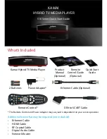
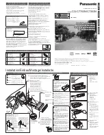
SPECIFICATIONS
POTABLE MD PLAYER
DMC-J3
SERVICE MANUAL
© 1998-3/B51-5411-00 (K/K) 3163
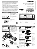
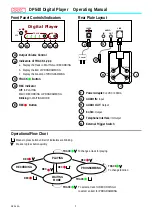
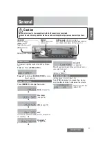
DISPLAY
VOL.
UP
V
O
L.
DO
WN
S
T
O
P
/ O
FF
PL
A
Y
/ P
A
U
S
E
POR
TABLE
MD PLAYER DM
C-J
3
TRACK NO.
BATTERY
7
£
¢
Ni-MH/ALKALINE
COMPATIBLE
4
DC I N
HOLD
OPEN
PHONES
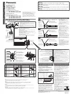
Knob*
(K29-)
Dressing panel*
(A21-)
Front glass
(B10-2407-04)
Lid assy*
(A53-)
Battery cover*
(A09-)
Dressing panel*
(A21-)
DC jack
(E03-0357-05)
Knob*
(K29-)
Knob
(K29-6828-03)
Blind plate
(F19-1086-04)
Knob*
(K29-)
Knob
(K29-6827-03)
Miniature phone jack
(E11-0381-05)
In compliance with Federal Regulations, following are reproduc-
tions of labels on, or inside the product relating to laser product
safety.
KENWOOD-Corp. certifies this equipment conforms to DHHS
Regulations No. 21 CFR 1040. 10, Chapter 1, Subchapter J.
DANGER : Laser radiation when open and interlock defeated.
AVOID DIRECT EXPOSURE TO BEAM.
1. KENWOOD follows a policy of continuous advancements in development, For reason specifications may be changed without notice.
2. The full performance may not be exhibited in an extremely cold location (under a water-freezing temperature).
Notes
Notes
* Refer to parts list on page 17.
System ............................ Mini disc digital audio system
Read method .................. Noncontact optical reading system
(semiconductor laser)
Sampling frequency ...... 44.1 kHz
Audio compression ....... ATRAC (Adaptive Transform Acoustic Cording)
Number of channels...... 2 channels
Frequency response ...... 20 Hz to 20,000 Hz (
±
3 dB)
Wow & flutter ................ Less than unmeasurable limit
(
±
0.001 % W.PEAK)
Input/Output terminal .. Remote control/Phones jack
Rated power output ......
......
......
......
......
........
9 mW+9 mW
Power source
DC IN jack (4 – 5.1V)
: Specially provided AC adaptor
: Car battery adaptor (sold separately, DC-C70)
DC 1.5V : Commercially sold AA alkaline battery (LR-6) X 1
DC 1.2V : Specially provided rechargeable battery (NB-130) X 1
(Charging time : About 4 hours)
Battery life (Fully charge, with "auto PS" setting ON)
Specially provided rechargeable battery (NB-130) X 1
..........................
..........................
..........................
Approx. 5 hours
Commercially sold AA alkaline battery (LR-6) X 1
......................
......................
......................
Approx. 6 hours
•
At 0.5mW+0.5mW output (32
Ω
load ).
•
Standard value during continuous use/charging in an temperature of
25˚C.
•
Time of use may vary depending on battery maker, battery
type, use environment,
and temperatute.
•
Time will be shorter when "PS off" Mode is set.
Dimensions (not including protruding parts)
W :99 mm (3-7/8")
H :17 mm (11/16")
D :75 mm (2-15/16")
Weight (Net) ................ 115g (0.25 lb)
not including the accessory rechargeable batter
140g (0.31 lb)
including the accessory rechargeable battery
DMC-J3(K)1P(
98.4.25
19:57
y [ W
2