


In compliance with Federal Regulations, following are
reproductions of labels on, or inside the product relating to
laser product safety,
KENWOOD-Corp. certifies this equipment conforms to
DHHS Regulation No.21 CFR 1040.10, Chapter 1,
Subchapter J.
DANGER : Laser radiation when open and interlock
defeated.
AVOID DIRECT EXPOSURE TO BEAM.
*Refer to parts list on page 49.
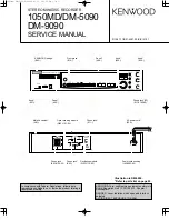
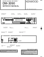
STEREO MINIDISC RECORDER
DM-3090
SERVICE MANUAL
© 1997-11/B51-5396-00 (K/K) 1812
MULTI CONTROL
TIME DISPLAY
DISPLAY/CHARAC.
TRACK/EDIT
ON/STAND BY
STEREO MINIDISC RECORDER
TIMER/
DELETE
ENTER
REC
REC LEVEL
0
10
PHONES LEVEL
MIN
MAX
PHONES
R
L
R
L
PLAY
OUT
REC
IN
DIGITAL
LINE
2
REC IN
1
REC IN
PLAY OUT
OPT.
RESET
KENWOOD badge
(B43-0302-04)
Front glass
(B10-2457-08)
Front panel
(A60-1370-08)
Knob (JOG)
(K29-6946-08)
Knob (REC/HP)
(K29-6947-08)
AC power cord bushing
(J42-0338-08)
AC power cord *
(E30-)
Optical digital output
(W02-2643-08)
Switch (RESET)
(S68-0091-08)
Analogue output terminal
(E63-1031-08)
Optical digital input
(W02-2643-08)
Knob (POWER)
(K27-2261-08)
Knob
(K27-2262-08)
Head phone jack
(E11-0345-08)
Panel
(A29-0898-08)
Digital input terminal
(E63-1032-08)
DM-3090(K)
COVER
97.11.29
0:18
AM
y [ W
2
Summary of Contents for DM-3090
Page 31: ...DM 3090 31 PARTS DESCRIPTIONS ...