HP F1523 - Pavilion - 15" LCD Monitor, Service Manual
Introducing the HP F1523 Pavilion 15" LCD Monitor with crystal-clear visuals and immersive display. To make the most of this cutting-edge technology, ensure you have the Quick User Manual at your fingertips. Download this essential manual for free at manualshive.com and effortlessly navigate your way to perfection.
Share
Download


Reviews:
No comments
Related manuals for F1523 - Pavilion - 15" LCD Monitor

XPR Series
Brand: Samsung Pages: 134
QB43R
Brand: Samsung Pages: 6

SH37F
Brand: Samsung Pages: 16

QB Series
Brand: Samsung Pages: 25
MB1
Brand: Federal Signal Corporation Pages: 20

HTK
Brand: Hamilton Pages: 135

XDS-2288
Brand: IAdea Pages: 9

DBJ Series
Brand: Samsung Pages: 156
KMC-W
Brand: Samsung Pages: 35
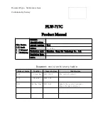
FLW-717C
Brand: Chang Rui Technology Pages: 40

DS-5525L
Brand: SunBriteTV Pages: 42

XDS-158 Series
Brand: IAdea Pages: 2
DVISplitter2-DL
Brand: G&D Pages: 24
VideoLine 4
Brand: G&D Pages: 16

Freestanding Multimedia Book Pod Display
Brand: Demco Pages: 3
DF-55
Brand: AG Neovo Pages: 33

Strada Transfer
Brand: Parkeon Pages: 42
SI-96 Series
Brand: IBASE Technology Pages: 50


