background image


HP Archive 


This vintage Hewlett Packard document was preserved 

and distributed by 

www. hparchive.com 

Please visit us on the web ! 


On-line curator: Louis Tabler 


Summary of Contents for 3320A

Page 1: ...HP Archive This vintage Hewlett Packard document was preserved and distributed by www hparchive com Please visit us on the web On line curator Louis Tabler ...

Page 2: ... l N M M 0 I OPERATING AND SERVICE MANUAL o o FREQUENCY SYNTHESIZER 3320A B o _C oO_ _ 2 1 1 e 0 o HEWLETTiii PACKARD I ...

Page 3: ...cts in materials and workmanship This warranty applies for one year from the date of delivery or in the case of certain major compo nents listed in the operating manual for the specified period We will repair or replace products which prove to be defective during the warranty period provided they are returned to Hewlett Packard No other warranty is expressed or implied We are not liable for conseq...

Page 4: ...to Serial Number 1I38A 00276 Model 3320A 1319A 00691 Model 3320B and higher Any changes made in instruments having serial numbers higher than the above number will be found in a Manual Changes supplement supplied with this manual Be sure to examine this supplement for any changes which apply to your instrument and record these changes in the manual Backdating information for instruments with lower...

Page 5: ...nse 3 3 3 34 Remote GPIB Programming 3 4 3 48 Handshake 3 6 3 52 Delay Flag 3 7 3 56 End Output 3 9 3 58 Reference Crystal Oven 3 9 Section Page IV THEORY OF OPERATION 4 1 4 1 Introduction 4 1 4 3 General Description 4 1 4 6 Simplified Block Diagram 4 1 4 7 introduction 4 1 4 9 Controller Section 4 1 4 11 Frequency Section 4 2 4 13 Amplitude Section 4 2 Section Page V MAINTENANCE 5 1 5 1 Introduct...

Page 6: ...1139A 00590 and Below 3320B 8 2 8 21 Change 9 for Serial Numbers 1138A 00275 and Below 3320A 1319A 00690 and Below 3320B 8 3 APPENDICES A CODE LIST OF MANUFACTURERS B SALES AND SERVICE OFFICES LIST OF TABLES Table Page I I Specifications I I 1 2 General Information 1 2 1 3 1 3 Accessories Supplied 1 3 1 4 Accessories Available 1 3 2 1 GPIB Bus Cables 2 3 3 1 Frequency Control Sertings 3 1 3 2 Ampl...

Page 7: ...iB Troubleshooting Tree 7 3 7 4 Reference Frequency Troubleshooting Tree 7 5 7 6 Figure Page 7 3 Frequency Generating Section Troubleshooting Tree 7 7 7 8 7 4 Amplitude Section Troubleshooting Tree 7 9 7 10 7 5 Controller Functional Block Diagram 7 11 7 12 7 6 Controller Configurations 7 13 7 14 7 7 Analog Functional Block Diagram 7 15 7 16 7 8 Common Assemblies Top and Bottom View 7 17 7 18 7 9 P...

Page 8: ...n 0 01 of range for 6 mo OoC to 5SoC Frequency stability Long term 10 parts in 106 of setting per year Vernier Out with ambient temperature reference Optional high stability crystal reference oven available Option 002 Signal to phase noise integrated 40 dB in 30 kHz band excluding 1 Hz centered on carrjer l0 MHz range Vernier Out Improves on lower frequency ranges Spurious 60 dB down Harmonic dist...

Page 9: ...el control not programmablel Output impedance 50 n 33208 AMPLITUDE SECTiON Amplitude range 26 99 dBm 1 2 watt to 69 99 dBm C 73 00 dBm under remote contrail into 50 n 26 99 dBm 5 V rms into SOn Amplitude resolution 0 01 dB Output impedance 50 n GENERAL 3320A B Operating temperature OoC to 55 0 C Storage temperature 40 0 C to JOoC J 2 75 Ohm Output Impedance Option 001 3320A B Attenuation and outpu...

Page 10: ...puts see resolution section of specifications These two ranges are fully programmable if digital remote options are installed F or field installation order accessory kit HP 11240A Field installable Q Except last vernier digit and line switch 1 12 ACCESSORIES SUPPLIED 1 13 Accessories supplied with the 3320A B are listed in Table 1 3 Table 1 3 Accessories SupDlied p Model ltv Description or Part No...

Page 11: ...aves the manufacturer with the 115 V 230 V switch in the 115 V position It is necessary to set the switch in the 230 V position when operating from a 230 V source Use the following procedure and Figure 2 1 for setting the 115 V 230 V switch a Disconnect power cord and slide the cover to the left to gain access to the fuse compartment Figure 2 1a b Remove the Line Fuse by pulling outward on the Fus...

Page 12: ... BCD source The remote input output connector is shown in Figure 2 3 A complete description of the input output signals and logic levels is given in Section III a Wrap the instrument in heavy paper or plastic before placing in an inner container b Place packing material around all sides of the instrument and protect the panel face with cardboard strips C Place the instrument and the inner containe...

Page 13: ...e used to interface the card reader to the 3320B If the card reader cable is hp Part No 0326Q 61605 the 11235A Adapter is Section 11 not required However the following card reader cable modification must be performed for proper operation 3260A CABLE 03260 61605 MODIFICATION For use with 3320B Option 007 1 Remove the four Screws holding the cover on the interface card on the end of the WI Cable 2 M...

Page 14: ...stability Short loop for 10 Hz Long loop for 10 Hz Paragraph J 121 AMPLITUDE Sets output amplitude from 26 99 dBm to 69 99 dBm Paragraph J 91 Output jack 3320A 1 V rms into 50 ohms 0 13dB con tinuous adjustment 3320B 5 V rms into 50 ohms_ 26 99 dBm 69 99 dBm 0 01 dB resolution LOW LEVEL OUTPUT Comes through 30 dB pad from output amplifier Amplitude follows electronic attenuatar 5etting 9 99 dB 2 3...

Page 15: ... dB are obtainable Each amplitude control operates indepen dently allowing changes of 0 01 dB 0 1 dB I dB or 10 dB in the output level Maximum output voltage is 5 V rms into 50 ohms or 10 V nTIS open circuit 3 12 Leveling 3 13 The 3320B frequency response is determined by the position of the LEVELING control For frequencies below 10Hz the LEVELING control should be in the OFF position This prevent...

Page 16: ...alt In t alutht Delay StQuence HOela In llatl InItIates he Delay Sl qutOCI 33201 B 2565A 3 18 33208 Amplitude 3 19 TI e 16 signal inputs prefaced A control the four amplitude digits and the sign of the amplitude The inputs representing each digit are as follows AIOOO A2000 A4000 A sign most significan t digit of amplitude polarity of amplitude Al A2 A4 A8 AIO A20 MO A80 AIOO A200 MOO A800 3 2 leas...

Page 17: ... OFF This will eliminate any distortion of the 3320B output caused by the leveling loop see Paragraph 3 12 If a frequency greater than 10Hz is programmed the leveling should be programmed ON 10 Hz 3 23 The signal input prefaced V and the four signal inputs prefaced VF control the vernier in out and the vernier frequency Programming conditions for vernier in out are HIGH out and LOW in Only the fir...

Page 18: ...sponse should be set to the slow mode delay code 3 1 DELAY FLAG 0 L J Ef o REF DELAY FLAG DELAY TIME VARIABLE See laDle 2 Figure 3 3 BCD Timing Sequence 34 Model 3320A B Table 3 2 Amplitude and Frequency Settling Times Delay Time of Range Amplitude Code Interval Frequency Tolerance Tolerance 0 15 ms 01 1 GOms 001 2 300ms i 3 1500 ms within rated accuracy Response in slow mode See Paragraph 3 33 3 ...

Page 19: ...ormally the ASCII character 3 octal code 063 but may be changed by means of internal jumper wires on the GPIB Input Assembly A37 Instructions for changing the address are given in Note 2 Figure 7 14 Table 3 3 lists the different addresses which can be assigned 3 40 An H preceding a mnemonic indicates that the signal is HIGH true L indicates LOW is true For example L DAV indicates that a LOW true s...

Page 20: ... Hz DELAy 1500ms LEVELING ON 10 Hz If there is no jumper between points A and B on the A38 assembly the 3320B will go to the previously remote programmed conditions when programmed to the remote mode The 3320B leaves the factory with no jumper 346 The second step in GPIB programming is the func tion programming This is accomplished by applying the ASCII code representing the information desired to...

Page 21: ...ta lines At the end of the count sequence the clock outputs a flag to the external controller delay flag or RFD This flag can be monitored to determine the accuracy which the 3320B frequency and amplitude has settled Table 3 7 lists the delay codes the clock time interval and the tolerances which the frequency and amplitude have settled The programmed delay code must be followed by a Delay Initiat...

Page 22: ...fast controller sets DAV HIGH T 2 T4 Determined by delay if programmed RFD LINES I I I To RFD T INSf I i i l IL_ lNST 2 i l i Li J_ __ t j l t J INST 3 INST 4 I I I DAC LINES I I I I i J l J To Fastest instrument is ready for data GPIB BUS 3 8 T 3 Slowest instrument has accepted data and the data can be removed T 4 Fastest instrument has accepted data T 9 Slowest instrument has processed data and ...

Page 23: ...the GPIB bus lines When this line is set low by the controller the 3320B and all other instruments paralleled to the bus lines will set all data lines MRE DAV RFD and DAC HIGH 3 56 End 0utput 3 55 The delay code programmed also controls the level ing mode of operation Delay Codes 0 3 LEVELING ON 10Hz Delay Code 4 7 LEVELING OFF 11 e programmed frequency or group of frequencies must be considered w...

Page 24: ...cesses information from the front panel controls or the remote inputs into BCD codes for controUing the frequency in the 3320A B and amplitude in the 3320B As shown in the Controller Configuration diagram Figure 7 6 the com plexity of the controller section varies with rhe 3320 Model and Options Refer to Paragraph 4 19 for a detailed block discussion of each t ontroUer type 4 6 SIMPLIFIED BLOCK DI...

Page 25: ...on The 3320B also has a 10 dB step attenuator at the output for 90 dB of level control 4 15 Reference Section 4 16 There are two frequency references in the 3320A B the 20 MHz Reference Oscillator and the Vernier Oscillator see Figure 4 3 When the VERN IN OUT control is in the VERN IN position the Vernier Oscillator is the source for the VTO and phase lock circuitry The 20 MHz Reference Oscillator...

Page 26: ... the front panel or remotely with parallel BCD lines as outlined in Section III of this manual In local control front panel the BCD code representing the frequency range and vernier in out setting are converted in the BCD control circuits The converted BCD code from the BCD control circuits is applied to the frequency section through the An Cable Board In remote control mode the BCD information fr...

Page 27: ... ASCII character 3 octal code 063 but may be changed as outlined in Section III The 3320B GPIB option is directly compatible with the hp 9800 series calculators The hp 3260A Marked Card Programmer may also be used as the remote controller 4 27 GPIB Bus Connections A principal advantage of the GPIB bus system is that all information is routed over the Model 3320A B same 15 lines For this reason sta...

Page 28: ...the 3320B The 9 s complement of a number is a Section IV number which when added to the first number equals nine For example the 9 s complement of a BCD 2 is a BCD 7 since 2 7 9 The BCD data for the amplitude settings is added to a preset BCD number in the BCD Circuits This BCD addition provides the proper BCD numbers for controlling the amplitude reference and 10 dBI step attenuator in the amplit...

Page 29: ...re it cal be placed in remote cOlltrol Model 3320A B 4 40 Local Control In local control the BCD circuits process the BCD data coming from the front panel settings switch closures to ground The input controller and latch circuits have no function during local control The 33208 GPIB option may be put into local control by one of the following methods I Initially applying power 2 By giving a Local E...

Page 30: ... 4 46 Range Dividers The output signal of the VTO is applied either to the amplitude section or to a series of range dividers depending on the position of the range control Seven ranges are available on the 3320AjB including Option 006 Table 4 1 lists the range positions the number of range dividers used for each position and the output frequency of each range divider 4 47 With the range control i...

Page 31: ... C 1 to discharge through R 1 When the counter has couoted the length of time allowed by the BCD signal switch B is opened and switch C is closed The de voltage remaining on C is transferred to holding capacitor C From C the de level is applied to the Modulator as a pretune dc and the Leveling assembly 4 53 The Leveling assembly consists of a thermopile circuit and a comparator see Figure 4 13 The...

Page 32: ...B of attenuation in 0 01 dB 0 1 dB or I dB steps These two altenuators work in conjunction to cover the 3320B range of 26 99 to 69 99 dBm At 26 99 dBm both attenuators are applying odB of altenuation When altenuation is added the first 9 99 dB is from the leveled 20 MHz Then at 16 99 dBm the 10 dB step altenuator will supply 10 dB of attenuation and the leveled 20 MHz is back to 0 dB of altenuatio...

Page 33: ... Option 007 in the 3320B With all programming options a BCD 8 4 2 1 signal is applied to a D A converter on the Vernier Oscillator assembly The de voltage from the D A is applied to the oscillator to vary its output frequency 4 62 UNIUUE CIRCUITS 4 63 3320B Thermopile Circuitry 4 64 When the 3320B LEVELING is 0 10Hz the AC DC converter monitors the output of the power amplifier see Figure 4 13 The...

Page 34: ... Figure 4 10 for the block diagram of the VTO Phase Lock Loop containing the N Counter The purpose of the VTO Phase Lock Loop is to provide an output frequency to the amplitude section The range of the output frequency from the VTO depends on the position of the vernier control switch voltage at TP2 exceeds about 2 5 volts IC5 sets the Monostable Flip Flop This causes K2 to close shorting the conv...

Page 35: ... as shown in Table 4 3 4 73 The N Counter utilizes three preseHable decade counters and the control circuits shown in Figure 4 19 The presettable counters and the A Flip Flop are set to a preset number by the BCD control lines The counter starts counting the VTa cycles starting with the preset Model 3320A B number The N Counter counts up to a maximum number of 3999 Sense No Each time the 3999 numb...

Page 36: ...ps Gates Sequence B A IC5 IC4 IC3 C D E F G Remarks BCD BCD 2 1 Preset 0 0 0 0 Enabled Disabled Start of Cycle Number Preset 1 t t t t t t 3990 1 1 9 9 0 0 Enabled Gate G Enabled 1 1 9 9 0 1 1 1 1 9 9 1 0 3993 1 1 9 9 1 1 0 0 0 Enabled Enaoled 3994 0 1 0 0 Disabled Disabled Counters and F F 1 are preset F F S is cleared 3995 0 1 1 0 3996 0 1 1 1 Output to phase comparator goes high 3997 0 0 1 1 39...

Page 37: ...s C D and E until 3999 is reached At 3996 the output to the phase comparator goes high and remains high until 3999 is reached Table 4 4 Preset Number Most 2nd Most 3rd Most Title Overrange Significant Significant Significant Digit Digit Digit Digit Frequency Control 1 2 6 5 Digits BCD Code of 1 0010 0110 0101 Frequency Control Digits Code to N Counter 1 0111 DOll 0100 Preset Number 0 7 3 4 The req...

Page 38: ...ing the performance test periodically vary the line voltage 10 with a power line transformer to insure proper operation at various ac line voltages When checking the performance of Option 001 use a 75 ohm to 50 ohm adapter on the output of the 3320A B excluding Para graphs 5 17 and 5 21 Refer to Figure 5 7 for part numbers and diagram of 75 ohm to 50 ohm adapter 5 7 Frequency Accuracy Vernier Out ...

Page 39: ... MHz hp Model 8553B 8552A Response 0 5 dB in 141Sdisplay Attenuator Attenuation 20 dB in 10 dB steps hp Model 3550 with known error Accuracy 0 01 dB Attenuator Attenuator 10dB in 1 dB steps hp Model 355C Thermocouple Input 3 V rms hp Model 11 049A Output 7 0mVdc hp Model 11 049 H01 Input Impedance 50 ohms and 75 ohms for Option 001 Double Balanced Mixer Frequency 100 kHz to 13 MHz hp Model 10534A ...

Page 40: ...Set the 3320A front panel controls as follows AMPLITUDE Full CW VERN IN OUT VERN IN RANGE 100 kHz FREQUENCY 010 0 c Set the 355D to J0 dB the 355C to 3 dB and adjust the wave analyzer for a 0 dBm meter indication at 10 kHz d Tune the wave analyzer to the second third and fourth harmonics of the 10kHz signal Harmonic levels should be at least 60 dB below the reference level set in Step c e Repeat S...

Page 41: ...r I 10 dBm whichever is greater NOTE The 2 i spurious for a 3320A B output frequency of i3 MHz is 7 MHz 40 MHz 33 MHz In Step c above be sure to check at 7 MHz with the wave analyzer 5 4 d Connect the equipment as shown in Figure 5 3 insure the 5 MHz osciJIator is at 5 000 000 0 Hz DO NOT EXCEED THE RA TED iNPUT OF MiXER e Set the 3320A B RANGE to 10 MHz and FRE QUE CY to 10 10 In 3320B set LEVELI...

Page 42: ...Hz oscillator until the channel A display on the oscilloscope is drifting very slowly f Ground the Channel B input terminal on the oscillo scope and adjust the display for a convenient reference Set the input terminal to de g Disconnect Channel B of the oscilloscope from point A Figure 5 4 and connect to point B h The oscilloscope display on Channel B should drift through 0 Vdc when the 3320A B si...

Page 43: ...nge This test also insures the 3320B meets the Frequency Response specification listed in Table I I from om Hz to 10 Hz The specification for the 5 6 3320A is 2 dB The specification for the 3320B is 0 5 dB referenced to 10kHz The total frequency response specification for the 3320B covers all frequencies at all settings of the 10 dB output level attenuator To test total frequency response of the 3...

Page 44: ...trols as follows AMPLITUDE Standard 26 99 dBm Option 001 24 99 dBm VERN IN OUT VERN OUT RANGE 10 kHz FREQUENCY 10 00 LEVELING ON 10Hz 5 24 This performance test insures the 3320B meets the attenuator accuracy specification listed in Table I I The specification is 0 02 dB IO dB step 10 kHz referenced to the straight through position of the output attenuator This specification is accumulative as att...

Page 45: ...been measured at all desired frequencies the recorded information is used in conjunction with the recorded information in Paragraph 5 21 and 5 23 to determine the frequency response of the IO dB attenuator Attenuatar dBm 2 4 6 8 10 12 14 16 18 Specification mVI accumulative 14 00 4 00 6 DO 16 00 26 00 36 00 46 00 56 00 66 00 15 00 5 00 5 DO 15 00 25 00 35 DO 45 00 55 00 65 00 Standard Option 001 b...

Page 46: ...wn in Figure 5 6 NOTE This performance lesl uses a 355D 10 dB atlenualOr with a known accuracy on the 0 dB and 10 dB settings The error in the attenuator should be used in delermining Ihe error ofIhe 3320B b Set the 3320B front panel controls as follows AMPLITUDE Standard 25 00 dBm Option 001 24 00 dBm VERN IN OUT VERN OUT RANGE 10 kHz FREQUENCY 10 00 LEVELING _ ON 10 Hz c Set the 355D to 10 dB an...

Page 47: ...eated for the 5 00 dBm attenuator step 3 Repeat the procedure Step g I for each of the remaining steps of the attenuator using the calculations of the preceeding steps for C in the formula 4 The frequency response specifications are as follows 33208 Attenuatar Settings dBm Specification Standard Option 001 LEVELING ON 10 Hz 26 99 to 24 99 to 5mV 3 00 5 00 3 01 5 01 to 12 mV 23 00 25 00 23 01 to 25...

Page 48: ...E ADJUST for a voltmeter indication of 10 V de 0 3 V de b Connect the de voltmeter to A3TPI Set the 3320A B FREQUENCY from 00 99 to 12 99 in I MHz steps The de voltmeter indication should not be more negative than 4V de on each frequency setting AI7pinB AI7pinC 29 125 to 30 875 28 800 to 31 200 5 35 Vernier 5 31 Reference Oscillator 5 32 This adjustment procedure sets the 20 MHz Refer ence Oscilla...

Page 49: ...RRIER NULL for minimum amplitude of the 32 99 MHz signal on the spectrum analyzer display g Return the green cable to the 20 33 MHz jack on the AID assembly Replace the brown cable to the Pre Amp output on the AID assembly 5 41 Amplitude 542 This adjustment procedure sets the amplitude section of the 3320A B for minimum temperature drift minimum de offset and proper output voltage level 3320B a Se...

Page 50: ...er to the 3320A front panel output jack Set the 3320A AMPLITUDE Full C W b Set the 3320B FREQUENCY to 12 99 RANGE to 10 MHz AMPLITUDE to 26 99 dBm 24 99 dBm Option 001 and LEVELING to ON 10 Hz b Remove the brown cable from the input of the A12A assembly Connect a jumper cable between AI2A 11 and ground c Adjust AI2ARII DC OFFSET for 0 V de 2 mV de indication on the de voltmeter c Adjust AI4R55 BIA...

Page 51: ...ltmeter indication c Set 3320B AMPLITUDE to 17 99 dBm 15 99 dBm Option 001 Adjust A9BR27 PRETUNE ADJUST for the same de voltmeter indication as recorded in step b d Adjusting A9BR27 effects the voltage indication at 16 99 dBm Repeat steps b and c until the two indica tions are within 200 mV de GENERAL MAINTENANCE INFORMATION 5 49 GENERAL MAINTENANCE INFORMATION 5 50 The following paragraphs cOhtai...

Page 52: ...move the ribbon cable from the A13 Switch Assembly and remove the front panel 5 53 Front Panel Disassembly 5 54 The following procedure provides information for disassembling the 3320A B front panel This will allow replacement of the switch wafers on the AI3 Switch Assembly On earlier 3320A B instruments the switch wafers were not replaceable Refer to the backdating Section VIII for serial number ...

Page 53: ...the frequency Range and amplitude switches as follows MSFD CW 2nd SFD LSFD 3rd SAD 2nd SAD LSAD gap in rotor blade is up See Figure below MSAD CW Range CW then CCW one position Hold Readout Disks in positions listed in Table 5 7 and tighten Allen screws 5 57 Impedance Cam Settings 5 58 The following procedures indicate the proper posi tioning of the impedance cams These cams are located on the 2nd...

Page 54: ...MS and COLLARS See Note MP62 MP62 f Ll1 i r 7tl 11 12 d Q 13 A 14 8 15 16 17 MP54 NOTE Cams and collars parts 17 18 19 20 fit on Readout Disks noted in parenthesis Figure 5 9 Front Panel and Vernier Control Mechanical Parts 5 17 ...

Page 55: ...litude Accuracy 50 Ohm load Open circuit Frequency Response 3320A 3320B 0 01 Hz l0 Hz 3320B 10 Hz 13 MHz Adjusted Errors PERFORMANCE TEST CARD 9999990 MH 12 219878 MH 1 099989 MHz 99 99900 14 000 kHz 12 9989 MHz 0 9 V rms 1 8Vrms 4 975 V rms 9 95 V rms 0 8 em 0 2 em 6930 N de Test Performed By _ Date _ 1 0000010 MH 12 220122 MHz 1 1000 1 MHz 100 00100 JlS 16 000 kHz 13 0009 MHz 60 dB 50 dB 50 dB 4...

Page 56: ...de 0 9B2 V de 1 002 V de 1 004 Vdc 1 006 V de 1 008 V de 1 010Vdc 1 012Vdc 1 014 V de 1 016Vdc 1 018Vdc Record Readings Step d 12 99 MHz I 01 MHz 11299 kHz 11 kHz I1299kHz 1 1 kHz I 12 99 kHz 1 01 kHz 15 5 5 15 25 35 45 55 65 Calculated Error Step g 1299 Hz I 10 Hz 15 5 5 15 25 35 45 55 65 12 99 MHz 01 MHz 1299 kHz 1 kHz 129 9 kHz 1 kHz 12 99 kHz 01 kHz 12 99 Hz 10 Hz Specification 5mV 5 mV 12 mV ...

Page 57: ...e di__ 1011 toggle tol 101er_ P peak trim trimmer pA etsl TSTA IrlinsiSlor pc printed circuit pF picof adls 10 12 tilfads V voltlsl piv pe in vallllge VilCW IIlternalir g CUITent wvorking vOIi plo part 01 v vlltiable pos position lsi vdc direct cur nt working voltage poly polystyrene pot pollntiometer Pi peak lo peak ppm p vts pe million prec prKision temperah l1 caefl t long Urm stability andlor ...

Page 58: ...ElECTEO FROM 2N37021 28480 1853 0020 AIQ3 1853 0020 TSTR SI PNPISELECTEO FRO 2 131021 28480 1653 020 AI l4 18 33 0020 TSTR SI PNPt SELECTED FROM 2N37021 28480 1853 020 A1 l5 1853 0020 TSTR St PNPISELECTEO FROM 2N37021 26480 1853 0C20 Al 6 1854 0019 16 TSTR SJ N 28480 1854 0019 AI l7 1854 0019 TSTR SI NPN 28480 1854 0019 AI l8 1854 0019 TSTR SI NPN 28480 1854 019 AIQ9 1854 0404 21 TSTR SI N 28480 1...

Page 59: ...fXO CER 0 01 Uf 80 201 100VOC 12 JS2 801 K800011 A2C6 0150 00 C FXO tEA 0 01 UF 80 Z 100VDCII 12982 801 K80oo11 A2C7 01S0 0e J3 C fXO tEA 0 01 UF 80 20t 100VOCW 12982 801 K800011 m 0ISO OC J3 C fXO CEil 0 01 UF 80 Z01 100VOC 12 J82 801 K800011 A2C9 0150 0093 C fXO CEil 0 01 UF 80 Z01 100VOCW 12982 801 800011 A2Cli 0180 174b C FXO ELECT 15 UF 10 20VDCW 28480 0180 11 b AlC 12 0150 0C84 21 C FJCD CE ...

Page 60: ...lM 5 11K OHN 1 810 28480 0751 0438 A2R32 0757 0438 R FXO N FLN 5 11K OHM i t 1 8W 28480 0757 0 38 A2R33 0157 0438 R FXO FL 5 11 K OHM 1 1 8 W 28480 0151 04 18 A2R34 0157 0438 R fXD N FLN 5 1ll OHM 1I8W 28460 0157 0 38 A2R35 0757 0442 R FXD MET FLM 10 K OHM 1 1 8w 19701 MF4CT O A2Tl 9100 1393 1 TRANSfORMER TOROID 28480 9100 1293 03320 66503 1 80ARD ASSY VTO 28480 03320 66503 A3Cl 0180 0291 21 C fXD...

Page 61: ...825 AlR15 0683 1535 R FXO COMP 15K OH 51 I W 01121 C8 1535 0 16 0157 04065 2 R FltD ET FLM lOOK OHM 11 1I8W 28 l O 0151 Io65 A Rl1 0151 0465 RtFltO MET FlM lOOK OHM 11 1 8 28 80 0151 0465 A 18 068 6825 RtFXO COMP 6800 OH 51 1 4011I 01121 C8 6825 A3R19 0683 1535 R FXO CO P 15K OH 51 1 4W 01121 C8 7535 A3R20 069 8 322 8 R FXO ET FLM 9 9K OHM 11 1 811I 2840 eo 0698 3228 A3R22 10698 3228 R FltO MET Fl...

Page 62: ... FXD MICA 430 Pf 5 300 VOCW 28480 0160 0939 A4e8 01SO 0093 e FXO CEll 0 01 UF 80 20t 100VOC 72982 801 K800011 A4C9 0150 0093 C FXO CER 0 01 Uf 80 2 0t 100VDCW 72982 801 K 800011 A4CI0 0150 0093 e D eER 0 01 u SD 20t 100VOCIII 72982 SCl KSOOOll A4C 11 01 50 0050 e D eER 1000 p 80 20 IOOOVOCW 56289 COb 7810 2E I 02l 526 COH A4C12 0150 0093 e D eER 0 01 u 8D 20t 100VOCW 72982 801 K 800011 Aloe 13 01S...

Page 63: ... 5600 OHM 51 114M 01121 C8 5625 1 41 3 0683 5625 R FXO COMP 5600 OHM 51 1 4111 01121 C8 5625 A4R 0683 6215 R fXO CO P 620 OHM 51 1 4111 01121 C8 6215 A4R5 0683 6215 R FXO COMP 620 OHM 51 114111 01121 C8 6215 A4A6 0683 1025 R fXO COMP 1000 CHI 51 1 4 1 01121 C8 1025 A4Rl C683 2015 R FXO COMP 200 OHM 51 114M 01121 C8 2015 4 1 8 0683 8215 II FXO COMP 820 OHM 5 1 4 W 01121 C8 bZ15 A4R9 0683 4115 II FX...

Page 64: ...S26 COH ASCII 0150 0050 C FXO 1000 PF 80 20 1000VOCw 5628 C0678102EI021S26 COH A5C15 C150 0050 C FXO cee 1000 PF 60 20 1000VOCW 56289 CQ618102E102ZS26 COH A5C16 0150 00 3 C FXO CER 0 01 UF 80 20 100VOCW 12982 801 K800011 A5Cl1 0150 0C50 C FXO CER 1000 PF 60 20 1000vOCw 5628 C0618102EI021S26 COH A5C18 01SO 0050 C FXO CEil 1000 80 20 1000VOCW 56289 C06781v2EI021S26 COH A5 19 0150 0093 C FXO CEil 0 0...

Page 65: ...5105 510 11 0683 9115 R FXO COMP 910 OHM 5l 1 4 01 01121 C8 9115 ASR 12 0683 1115 R FXO COMP 110 OHM 5Z 1 4W 01121 C8 1115 0 510 13 0683 4325 R FXO COMP 4300 OHM Sl 1 4 01121 C8 325 A5R14 0633 5105 Fl F O COMP 51 OHM SZ 1 4W 01121 C8 5105 1 510 15 0683 1125 R FXO COMP 1100 CliM SZ 1 4W 01121 C8 1125 1 510 16 0683 7515 R FXO COMP 750 OHM 5l 1 4W 01121 C8 7515 ASR 17 0683 1025 R FXO CO P 1000 OHM 5l...

Page 66: ...AL bd A1C25 C26 0160 2221 1 c FXO MICA 1300PF5 72136 ADM19F132J3C A7 C27 0180 1746 C FXO 15 UF 10 20 VOCw 56289 1500 156X9020B2 0 YS A7CR1THRUCA6 1901 0040 6 DIODE 51 50 A 2 PF 2 NS 30 v 07263 FOG10BB AllC 1 1820 092319 I IC DUAD 2lNPUT NOR GATE 04713 5C7521PK AlIC2 IC3 IB26 0043 1 Ie llNEAR OP AMP 12040 Sll2795 Al1C4 1820 0595 IC DUAL DIGITAL 12040 DM74L7 iN AHI 9100 3314 I COIL MOLDED 28480 9100...

Page 67: ...VOCW 72982 801 K800011 ASCL8 0IltC 0222 C fXO MICA 00 11 300VOCW 28480 0140 0222 I 8CI9 0150 0122 C FXO CER 2000 PF 20 500VOCw 72982 8 1 000 Y5S 202 ASC20 01so oe93 c no CEFt 0 01 UF 80 20 100Voew 72962 8CI K800011 A8C2t 0150 0C J3 C FllO CER 0 01 UF 80 20t 100Voew 12982 801 K800011 A8C22 0150 0122 C fllO CER 2000 500VOCW 72 J82 8CI 000 Y5S 202M A8C23 0150 0122 C FllO CER 2000 20 iOOVOCw 72982 801...

Page 68: ... C6 5625 A8Rl5 0683 6215 R FXD C C P 620 OHM 52 1 410 01121 C6 6215 A8R16 0683 6215 R FXQ COMP 620 OH 5 1 1 4101 01121 C6 6215 A8R17 0683 1025 R FXD CO P 1000 OHM 5 1 4W 01121 C6 1025 A6RlS 0683 2015 R FXD CQI IP 200 OHM 5 1 1 4101 01121 C6 2015 ASF 19 C683 3315 R FXD CO P 330 OHM 52 1 tW 01121 C6 3315 A8R20 0663 1035 5 R fXD CCI IP 10K OHM 5 1 1 4101 01121 C6 1035 A8R21 0683 2025 R FXD COMP 2000 ...

Page 69: ...0 35 VDCW C FXO TArn l0 UF 10 20 VOCW C FXO ELECT 0_68 UF 10 35 VOCW C FXO ELECT 0 1 UF 10 35 VDCW C FXO MICA MY 0 0022 UF 10 200 vocw c FXO MICA MY 0 0022 UF 10 200 VOCW C FXO HECT 0 1 UF 10 35 VOCW C FXO MY 0_0068 Uf 10 200 Vocw C FXO elECT 0 1 UF 10 11 35 VOCW C FXD CER 0 01 Uf 80 20 100 VDCW C FXD CER 0 01 UF 80 20 100 VOCW C FXO CER 0 01 UF t 811 20 1110 VOCW C FXO MICA 51 PF 5 C FXD CER 0 01...

Page 70: ...HM 5 1 4 W A FXO FlM4 12K OHM l I SW R FXO MET FlM 22 6 K Of iM 1 1 8W R VAR FlM 2000 OHM 0 LIN 1 2 W R FXO MET FlM 3 01 K OHM 1 1 8W R FXO METFU 499 OHM 1 1 8W A FXO MET HM 499 OHM 1 1 8W A FXO MET FlM 499 Of iM 1 l SW A FXO MET FLM 5_11 K OHM 1 1 8W R FXO FLM 10 2 K OHM 1 1 8W R FXO FLM 165 OHM J 1 8W R FXO MET FlM 1 K OHM 1 1 8 W R FXO MET FLM 5 62 K OHM 1 1 8W R FXO MET FlM 2 14 K OHM 1 1 6W R...

Page 71: ...TQR Rf SUB MINIATURE SERIES 98291 52 053 0000 AIOJ2 1250 1195 CONNECTOR RF SUA JIlINIATURE SERIES 98291 52 053 0000 AIOLl 9140 0106 2 COll FXO 0 oCo7 UH 28480 9l1tO Ol06 AIOl2 9140 G098 COIl FXD RF 2 2 UH 28480 9litO 0098 AIOl 9HO OI06 COIL FXO 0 47 UH 28480 9140 0106 AIOL4 9lito OU4 CoIL FXD RF 10 UH 28480 9140 0114 AIOlS 9100 1620 COIL HOLOED CHOKE 15 0 UH 10 28480 9100 1620 AlOl6 9100 3316 1 CO...

Page 72: ...1 8W R FXO FLM 432 OHM 11 1 8W R FXO MET FLM 5 11K OHM 11 1 8101 R FXO MET FLM lo 02K OHM II 1 8W R FXO MET FLM 10 OK OHM 11 1 8W R FXO MET FLM 10 OK OHM II I SW R FXO CO P S60K OHM 101 1 4W R FXO MET FLM 4750 OHM II I SW A FXO MET FLM lo9 9 OHK I 1 8101 R fXO COHP 560 OHM 10 1 4 R FXO MET FLM lo9 9 OHM 11 1 8W R FXO MET FLM 49 9 OHM II I SW R FXD MET Hili lo99 OHM 11 1 8W R FXO MET FUt 40 2 OHM 1...

Page 73: ...C8 2225 AllR22 0698 toolt8olt R FlO Flt 19 IK QHM U 1 811 28480 06098 4 to84 AllR24 0683 2225 R FXO CaMP 2 21 OHM 1 tow 01121 C8 2225 AllR25 0683 1525 R FXD CC P 1500 OHM 1 411 01121 C8 1525 Allil 26 0683 5635 1 R FXQ CCMP 56K OHMS l loV 01121 C8 5635 A111t21 0683 102S R fXO CCMP 1000 OHM 1 toW 01121 C8 1025 AllR28 06e3 1025 R FXO COMP 1000 OHM 5l 1 4W 01121 C8 1 l2S AllR29 0683 2235 1 11 FXO CO P...

Page 74: ...9701 0698 34 1 0 157 0395 CMF l IO 32T l CMF l 10 32 T l 2100 2583 CMF 1I10 32T l C84701 07S7 0H8 0698 4195 caB201 0698 082 C8 4101 0696 4452 0757 0284 M F4C T O bd bd A12 R19 A 12 R20 A12 11 21 0757 0346 0757 0346 0151 0389 R FXO HET flM R FXO HET FLM R fXO FLM 33 2 10 OHM U 11611 10 OHM 1 t 1 8 OHM It lIBW 28 8C 28480 19701 0757 034b 0757 0346 MF4CT 0 A12 ll 22 A12 R23 A 12 ll 24 A12 ll 25 A 12 ...

Page 75: ...7 MEGOHM lOt 1 411 01121 4751 All 6 068 2251 0 COMP 2 2 MEGOHM 1 4101 01121 e6 2251 All 7 0698 44 1 0 FLM 54 9K OHM 1 1 811 28480 0698 4499 All 01 8 8004 2 0 FLM 200K OHM O I 1 8101 28480 06 8 8004 All RiD 2100 3056 2 A CERMET 5K OHM TYPE P 3 411 28480 210Q 3 56 A12 12 0698 8004 0 FlM 200K OHM 0 1 1 811 28480 0698 8004 All 13 0757 0412 2 0 MET FU 200K OHM It 1 8W 28460 0157 0472 All 14 0151 0412 0...

Page 76: ...71 3130 0473 MSFll DETENT 28480 3130 0473 3130 0472 2ND SFD WAFER 28480 3130 0472 3130 0477 2ND SFD DETENT 28480 3130 0477 3130 0472 LSFD WAFER 28480 3130 0472 3130 0477 lSFD DETENT 28480 3130 0477 3130 0476 MSAD W FER 28480 3130 0476 3130 0479 MSAD DETENT 28480 3130 0479 3130 0472 3RD SAD WAFER 28480 3130 0472 3130 0477 3RD SAD DETENT 28480 3130 0477 3130 0472 2ND SAD WAFER 28480 3130 0472 3130 0...

Page 77: ...C FxO ELECT 6 8 UF 10 3SVOCW 56289 1500h85X903S6Z 0YS Al4t31 0180 02e n C FXO ELECT 1 0 10 35VOCW 56269 1500105X9035A2 0YS A1406 0180 0291 C FIlD ELECT 1 0 UF 10 5VOCW 5628 150010SX903SA2 0YS Al4C39 0180 0291 C FXD ELECT 0 0 3SVOCW 56269 150010SX9035A2 DYS Al C40 0180 0291 C FIlO ELECT 1 0 Uf 10 3SVOCW 56289 1500105X903SA2 0YS A14 41 019 0 76 C FXO ELECT 0 41 UF 10 I VDCW S6289 150D41 oX9035A2 0YS...

Page 78: ...OHM I l aw 28480 0751 0 42 AHiU6 0751 038lt 0 FL 20 OHM l 1 8W 28 80 0757 038 A14R17 0157 0291 0 FL 24 9 OHM U 1 811 28480 0757 0291 Al4R 18 0757 07 7 2 0 F L SilO OHl1 U 1 4W 28480 0157 07 7 Al RI9 0757 0428 D ET FLM 1 62K OHM 1 1 811 28 80 0157 0 28 AIlWt20 0698 135 1 0 H T FLM 8 87K OHM I O 1 2W 28480 0698 135 Al R21 0757 0271 FXO HET FlM 4 1 9 OHM U 1 8 11 28480 0757 0211 t AI4R22 01S1 0217 FX...

Page 79: ...D PREC FlM 241 5 OHM 1 1f4W 01138 CMF 60 1 T9 A1511 14 069B 7984 R fXO fLM 61 1 OHM on 112w 28480 0698 7984 A15R 15 0698 1984 R fXO fLM 61 1 OHM 01 112w 284BO 089B 7984 A15R16 089B 8258 R fXO PREC FlM 247 5 OHM 1 1 4W 01738 CMf 60 1 T9 AI5RI1 II 18 0698 7984 R fXO fLM 61 1 OHM 0Uli II2W 28480 069B 7984 AI5R19 0698 8258 lI fXO PREC FlM 247 5 OHM 1 1 4W 01138 CMF 60 1 T9 Al5it20 06 S 7981t R fXD flM...

Page 80: ...W 28480 0151 C429 AI7R4 0698 3219 NET FLM 0990 OHM U 1 8W 28480 0698 3279 A17RS C698 3219 MET flM 0990 OHH II 1 8W 28480 069l 3279 AllR6 068 1041 1 CaMP lOOK JiM 0 1 4W 01121 C8 1041 A17R1 0151 028 FXD Hel flM 150 OHM 1 1 1 8W 28480 0151 028 A17R8 0811 1200 2 fXO WW 0 10 OHM 101 2w 28 480 0811 1200 11R9 0811 1200 WW 0 10 HH I 2 28480 0811 1200 1 1111 10 0757 0 401 MET HM 100 OHM 1 8W 28 080 0757 0...

Page 81: ...HM 51 1 4W R FXO ceNP 2700 OHM 51 1 4W 80ARa ASSY INTERFACE B IC OIGITAL TTL HEX CONVERTER IC OIGITAl TTL HEX CO VERTER IC OIGITAL TTL HEX CONVERTER IC MOS Ie NOS IC 1405 Ie 1405 IC OIGITAl TTL QUAD 2 1NI T EXCL OR GATE IC TTl QUAD 2 INPT NOR GATE IC TTl TRIPLE 3 INPT NAND GATE IC DIGITAl TTL HEX CCNVERTER IC TTl QUAD 2 INPT NANO GATE IC DIGITAL TSTR SI PNP TSTR SI FET TSTR SI PHP TSTR SI NPNISELE...

Page 82: ... P 5100 OHM 51 1 4101 R FXD COMP 1800 OHM 51 1 4W R FXD eot p 2000 OHM 5 1 101 PC ASSY INVERTER IC TTL HEX INVERTER R FXO COMP 510 OHM 5 1 4 W A FXO COMP 510 OHM 5 1 4 W R FXD CDMP 180 OHM 5 1 4 W R FXD COMP 15 K OHM 5 lf4 W BOARD ASSY AMPLITUDE CONTROL C FXD CEI 0 01 UF 80 20 100VOCW C FKD CEI 0 01 UF 80 20 100VOCW FXO CEil 0 01 UF 80 201 100VOCW IC OIGtTAL TTL QUAL 2 WIOE INPT AND OR IC DIG1TAL ...

Page 83: ...aMP 1000 OHM 5t 1 R FXO CO I 1000 OHM 5t 1 4 80AR O ASSY PAIl LGC TSTR 51 NPNISELECTED FROM 2 1 1041 R FXD CCI IP 1500 OHM 5 1 R FXD CCI I 1500 OHM 5 1 4 R FXD eOMP 3900 OHM S 1 4W R FXO eOMP 3900 OHM 5 1 4 W R FXO CaMP 1500 OHM 5 1 4 W R FXO CaMP 1500 OHM 5 1 4 W R FXO COMP 3900 OHM 5 1 4 W R FXO eOMP 3900 OHM 5 1 4 W R FXO eOMP 1500 OHM 5 1 4 W R FXO eOMP 1500 OHM 5 1 4 W R FXO COMP 3900 OHM 5 1...

Page 84: ...21 C81525 A28A83 0683 3925 A FXO COMP 3900 OHM 5 1 4 W 01121 C83925 A28R84 0683 I 525 A FXO COMP 1500 OHM 5 1 4W 01121 C81525 A28R85 0683 3925 R FXO COMP 3900 OHM 5 1 4 W 01121 C83925 A28R86 0683 I 525 R FXO COMP 1500 OHM 5 114W 01121 C81525 A281181 0683 3925 R FXO COMP 3900 OHM 5 1 4 W 01121 C83925 A281188 0683 1525 R FXO COMP 1500 OHM 5 1 4 W 01121 C81525 A28R89 0683 3925 R FXO COMP 3900 OHM 5 1...

Page 85: ... 0683 1025 R FXD CDMP 1 KOHM 5 1f41Y 01121 CB 1025 A31A25 0683 1535 0 0 caMP 15K5 1 41Y 01121 CB 1535 A37A26 06833615 0 0 COMP UoOHM 5 1I4 V 01121 C83615 A37RH 0683 1025 0 caMP 1 I OHM 5 1 4 Y 01121 CB 1025 A37R28 0683 1035 0 0 COMP 10 K OHM 5 1I4W 01121 ce 1035 A31R29 0683 1025 0 0 COMP I I OHM 5 1I4 Y 01121 CB 1025 A37R30 0683 1535 0 0 COMP 15K 5 4W 01121 ca1535 A37R31 0683 3025 0 0 CaMP 3KaHM5 ...

Page 86: ...C 30 2X151 CONTACTS 76530 65 7160 CHASSIS MOUNTED COMPONENTS CI 0180 2397 I C FXO 18000 UF CRI CR2 1901 0526 3 ASSY OIOOE 8R lOGE SI 100 PIV 51 CR3 1901 05 16 ASSY DIODE BRIDGE Sl100 PIV SA Fl 11QVac 2110 0312 I FUSE lA 250 V SLO no FI 230 Vac 211Q 0202 I FUSE 0 50A 250 V 510 BlO 75915 313 5005 F2 2110 0055 I FUSE 411 250 V NO RMAL no J1 THAU J5 1250 1194 CONNECTOA RF SUBMIN J 1250 0252 CONNECTOR ...

Page 87: ...32Q 24707 1 SPACER BAR MPH OJJzo 2 108 1 SPACER ROO MPI8 SCJ6G 8513 1 COVER SOTTOM MP19 03320 64301 PLATE SWITCH MP20 MP20 Front PaOlI Assembly Inclod A13 S itch Assembly 03320 60302 PANEL FRONT 3320A 03320 60304 PANEL FRONT 3320A OPTION DOn 03320 60301 PANEL FRONT 3320S 03320 60303 PANEL FRONT 3320S OPTION 0011 MP21 5020 6856 TRIM BOTTOM MP22 0310 2257 8 t NOB RND m 0310 1092 KNOll 1 2 RNO MP24 0...

Page 88: ... INT I 03320 220 11 7 GEAR 3EVEl 2100 2217 1 R VARWN LIN 10 K OHM 5 3W ID 1140 0053 1 COUNHR 11 ISJO I638 I POINTER 12 1430 0741 1 GEAR CfNHR SPUR 13 0332 1 24706 I SPACER GEAR U 2190 0378 2 WASHER s s_ 15 03320 23101 I SHAFT BEVEL GEAR 219lHlB19 2 WASHER NYlON 17 504 5878 1 CAM 28480 5040 5878 18 0332 26202 1 COLLAR 28480 0332 26202 19 5040 5946 1 CAM 28480 5040 5946 20 03320 26201 1 COLLAR 28480...

Page 89: ...MP1 w w T1 I MP26 I MP25 m x s m n r MP15 MP14 1 2 MP11 MP12 MP10 MP9 MP6 MP HO O ee o 0 g W W 2 f o 5 ...

Page 90: ...0 W c S C l o n r f 3 20_ 8 l 81 7 r Ji t See Appendix C Manual Backdating Rev A For I nslrument Serial Numbers 3320A 1121 A 00111 and above 33208 1122A 00121 and above MP34 MP32 g o S o 0 g W w 5 ...

Page 91: ...LARS See Note MP62 9 f MP20 8 It 3 4 7 r n 7 P c ifP 7 I 6 11 12 5 13 14 rf 8 15 16 17 MP54 NOTE Cams and collars parts 17 18 19 20 fit on Readout Disks noted in parenthesis Figure 6 3 Front Panel and Vernier Control Mechanical Parts 6 35 ...

Page 92: ...Frequency Trouble shooting Tree 7 6 SCHEMATIC OIAGRAMS 7 7 The schematic diagrams Figure 7 9 through Figure 7 32 contained in this section show the detailed circuits of the 3320AjB Components marked with an asterisk are those that are critical in value The value of these components may vary from one instrument to another The optimum value is selected at the factory All options available with the 3...

Page 93: ...T GROUND 5 DENOTES CHASSIS CIRCUIT GROUND 6 DENOTES POWER LINE GROUND 7 DENOTES SCREWDRIVER GRQUND 8 DENOTES ASSEMBLY 9 2 DENOTES SIGNAL DESTINATION 10 I DENOTES FRONT PANEL MARKING 11 J DENOTES SlDEAND REAR PANEL MARKING Model 3320A B 12 DENOTES SCREWDRIVER ADJUST 7 2 13 DENOTES WIRE COLOR COLOR CODE SAME AS RESISTOR COLOR CODE FIRST NUMBER IDENTIFIES BASE COLOR SECOND NUMBER IDENTIFIES wlDER STR...

Page 94: ... C 103 0 0 D O 0 0 0 0 0 0 0 0 0 0 0 0 0 0 CJ O 0 0 0 0 0 0 0 0 0 0 I ua son I alOI 2 00 IIOT _ SH IOUlAIIU to 3 lUX COWlan 4 lM DI I lHISSIOE _ J WI C RO NO I agnortic C d 5 m 00 00 100 40 0 0 0 0 0 0 0 0 0 0 0 0 0 0 0 0 0 0 0 0 0 0 0 0 0 0 0 0 0 0 0 0 0 0 0 0 0 267 0 _ 0 _ 0 o c 0 0 0 0 0 A 101 0 _ 0 0 0 0 OS3 0 0 _ 0 2 062 0 0 0 0 0 0 _ 0 0 0 _ 0 I 0 0 _ CJ _ 0 054 0 0 _ 0 0 0 F 0 _ 0 0 0 _ 0 0...

Page 95: ...u card In tht Card Ruder OJ Whilth Card Reader is running the Iogit probe Indit iluon should cOlTtspond with thl sewnd digll of the code btlngthec ked El hen the Card Ruder 11M 5l0Pped running th loglt probt Indiution should cornepond Wllh the Ihird digll of the code ng thttked F If the logiC probe mdlCillton iSI lCorrttt lor ilny or I digits 01 iI g coM replate the boiIrd tndlQlld in the Logic Tr...

Page 96: ...ot correct replace A23 If the code is correct go to Step d Are pin states as shown inTable 2 b Insert Diagnostic Card No 1 a Connect logic probe to XA37 pin L b Check pins listed in Table 2 with logic probe a Insert Diagnostic Card No 2 RepiaceA37 Is XA36 pin 15 high lsXA24 pin Y high b Check pins listed in Table 1 with logic probe a Insert Diagnostic Card NO 1 Go to 3260A Troubleshooting Trees a ...

Page 97: ...N fIGURE2 O GURE2 ONLY 3 9 L t _Y_e_s l g_NI z SCOPE TO AT PIN _ I _ S GR iU SNI IG Uf 6 CE AT WITH NEW 20 Hz tNo j Yes AT AT PIN 10 2 MHz IS REMOVE AT fROM SIGNAL 3320A 3320B I a 2 MHz 20 Hz b AS IN fiGURE 3 BUT 4 2 V p p L AT Al PIN M 1l0 kHz a ODES F VARY fROM _ I __ 10 000 kHz TO AT LEAST 10 003 kHz b IS SIGNAL AS IN fiGURE 11 5tiNM 4 SI U No PlITUOE 400 mV p p DC OffSET OVOLTS SET VERN INIVER...

Page 98: ... 5 V 3 5 V OV OV 1222 0 0 1 1 1 0 1 1 1 0 1 1 1 Any Range I TAlllE fREQUENCY SWITCH lOGIC ALL PIN NUMBERS ARE LOCATED ON W2 FREQUENCY PINS ON W2 SETTING 12 14 18 20 I 3 I 1 I 11 13 11 21 19 23 17 7 01 P gnd I open P P kH 0l en 888 P P open I gnd open kH PO open P PO PO PO PO 12 00 I I I MH TABLE 4 INSTRUCTIONS A lf you art TroublfShODling the JJ211B Dplion 001 you do not have A21 in the uni B If y...

Page 99: ...NO C O CHBO QRGri C A REMOVE A4 FROM 3320A _ ___ C Oi CHBO ORGri CA NO READ 111 00 KHz 1 0 Hz LEVELS AS SHOWN IN TABLE 3320B LEVELS AS SHOWN IN TABLE 11 1 g t06A DI CSEL6 GO TO AMPLITUDE SECTION NOTE SIGNAL MUST BE AM TROUBLESHOOTING TREE PLlFIEO BEFORE COUNTER CAN READ IT USE 461 WITH 40dB GAIN AT A6Jl IS F R E QUE N C YON C 0 U N T E R 20 001222 MHz AMPLITUDE 100 mV TO 800mV p p DC OFFSET oVOLTS...

Page 100: ...0 0 1 I 1 0 0 0 1 0 0 1 2366 dBm I 0 1 1 0 0 1 I 1 1 0 I 1 1 0 TABlE 2 lOGIC fOR A15l0GIC CONNECTOR AMPLITUDE lOGIC WEIGHTS I SETTING 4 2 2 1 I 2500 dam JVlo 5V JVto 5V Vto SV JVto 5V 1 1 1 1 6500 dBm DVIO 6v QV10 6V OVlo 6V OVlo O 6V 0 0 0 0 UBlE 3 AMPLITUDE SWITCH lOGIC All PIN NUMBERS ARE LOCATED ON Wll AMPLITUDE PINS ON W2 SETTING I 21 28 lO 11 J2 33 J4 3S 36 J 38 39 40 41 42 11 17 open open o...

Page 101: ... TO OFF B REMOVE THE CONTROL LER ENO OF THE FLEXIBLE PLASTIC CABLE IW2 WHICH CONNECTS THE FRONT PAN CHECK THE LOGIC LEVELS EL TO THE CONTROllER ON THE CONNECTOR FROM 0 C USE LOGIC PROBE OR __ WHICH A15 WAS REMOVEO _ _ _ OHM METER TO MEASURE l ARE LOGIC LEVELS AS IN ARE THEY AS SHOWN IN CONTACT CLOSURES TO TABLE 3 TABLE 2 GROUND FOR EACH AMPlI TUOE SETTING ANO PIN NUMBER IN TABLE 3 MAKE MEASUREMENT...

Page 102: ...38 pin 3 I 1 0 0 1 0 0 1 H Local Enable lCll pin 101 K 1 0 0 0 0 1 1 H Vernier In XA38 pin 01 M 1 0 0 1 1 0 1 H Vernier Out XA38 pin 4 R 1 0 1 0 0 1 0 L RANGE XA38 pin E V 1 0 1 0 1 1 0 L Vernier Digit XA38 pin B Positive True X Don t Care NOTE This is a Functional Block Diagram of the GPI B and BCD Controller The logic symbology shown is functional and may not agree with the conventional Logic sh...

Page 103: ... TO 0 AND SIGN FF TO I l l I _ _o_ _ _ O_ _ _ II _ _ _ __ I _ _ _ _ AMPLITUDE 1 j r i C13 IF SELECTS IC 14 STORAGE Ol t ICIS IC3 5 CLEAR K CLOCK IC6 RI R2 FUNCTION EXECUTE o jJ H STROBE I PREFACE I OMMAND LOCKO CUT71 f c 9 Jc I 3 I IH NO STROBE DELAY INITIATE ENABLE I C CODE 103 _ ICB PIN I H NUMERAL NO ENAtlLE 1060 071 CODES I IC 16 1f 1 I IC 17 V I T TPi 3 __ 2_ _5 G_P_1 B_L_A_T_CH_E_S__ j l I L...

Page 104: ...ER ASC II INPUT OUTPUT 3320A OPTION 003 BCD 3320B OPTION 004 BCD BCD INPUT OUTPUT L _ _ CONTROLLER BCD INPUT OUTPUT CONTROLLER 3320B STANDARD OPTIONS 001 002 OR 006 3320A STANDARD OPTIONS 001 002 OR 006 CONTROLLER Figure 7 6 Controller Configurations 7 13 7 14 ...

Page 105: ...3 20 33 MHz Out Rear Panel Low Level Out Rear Panel 1 MHz Out Rear Panel 10 kHz see waveform l T v PodOd j U L IOO uc The VTO frequency varies between 20 MHz and 32 99 MHz depending on frequency set ling NOTE Use a 10 1 probe and a counter with high sensitivity hp 5245L with 5261 AI when measuring frequency at A3TP3 6 V p p when unlocked see Reference Oscil lator Adjustment procedure section V 20 ...

Page 106: ...OCAL REMOTE REMOTE ILOCAL lOUT I I I r J _T _0 I MHz _10 2 t c c 400e l L _ _ _ _ _ J II I MHz I 1 7 2 REMOTE STANDJD OPTIONS I ENABLE OPTIONS 001 L 003004 I 20 MHz I ffi 00 iz 06 RZ n I if _T PI V CONTROLLER FUNCTIONAL I PHASE DC I BLOCK r VAMPLIFIER COMPARATOR 7MPLIFIER 1 1 1 1 l _ DIAGRAM 19 t I L C J c o RN OU 7 1 VERN I I VERNIER 00 X VERNIER JUMPER CABLE FREOUENCY IN OUT ES EN L J OSCILLATOR...

Page 107: ...AI3A hp Port No 03320 61902 FRONT PANEL SWITCH ASSEM BLY 3320A B 3257 08 800 8888 3320A 5 B 2356 AI3B hp Po rt No 03320 61901 FRONT PANEL SWITCH ASSEMBLY ...

Page 108: ...xA20A STD3320B XA21A ASCII 8 BCO 3320A B X A2ZA OPTION 003 004 B 007 AI A XA2 I A XA3 A XA4 I XA5 I XAS I XA7 I XAa I XA9 I A XAIO I XAlf XAl2 I A I s 15 S S S IS 15 IS IS S IS AI9 hp Port No 03320 66519 Rev B MOTHER BOARD 3320A B 8 3259 ...

Page 109: ...fl45 f 44 R42 R43 R41 R40 R38 R39 R37 R65 R6 R68 A6 H69 R57 R r5 Rl4 R77 R76 R72 R70 R73 R71 R79 R7 RA9 R88 R85 R84 R81 RB6 R 3 R82 R3 RI R4 R2 DODDDDDDDDDDDDD OOOOOODUDDDO X 1 N OJ 1 ll o a o t aJ n o s g I tIl a z ii o O N OJ jJ X ll N i Ol a Ol Z J1 N a OJ a x t 1 t r lu L r Iu x l Xl l X l N UO l PoL 1 r Iu r Iu x l tv j l Nil N x t l Nil J 0 iii l m z 0 0 0 C10 o 0 l JJ o JJ N l 0 5 Z j o o J...

Page 110: ... I 1 I Jl I nr r i i l _ XA17 F2 I r J w u U A19 I C u II 81 II u u A13 U AC Power Module A39Pl A28Pl Oncludes Fl ASCII BCD 0 4 0 5 Rev A TOP VIEW BOTTOM VIEW RIGHT SIDE VIEW Figure 7 8 Common Assemblies Top And Bottom View 7 17 7 18 ...

Page 111: ... H L H L H L H H H H H H H H H H 5 1 0 1 0 H L H H H H H H H H H H H H 6 0 1 1 0 H H L L H H H H H H H H H H 7 1 1 1 0 H H L H H H H H H H H H H H 8 0 0 0 1 H H H L H H H H H H H H H H H H H H H H H H H H H H H H 9 1 0 0 1 n 12 34 I a 0 I a a U en I 0 N x 8 a 0 n I 0 a I z 10 I z G J N 0 a 0 a u I U 0 a u u 4748 4950 A 0000000000000000000000 3320A B 3084 I NOTE 2 On A20lC5 input at pin 12 is hard ...

Page 112: ... 4 I I I I I I I I I 16 TO XA2 PIN E 12 i T I i 10 I I I 9 IO IO S TO XA2 PIN J 12 I I 5V I 1 1 I RIF FREQUENCY I I 1 2 7K 1 I 5V 10 20 Rrr 1 1 8 lr 0 53 i1 1 I III K o y j Jf 4 0 I rigm if L __ l _ _ 3 80 14 t ig T 80 I f5 2G i l 2 7K I 100 14 100 P t ig nll N If g i I 1 1 I 14 oo20 9 ICI X1 2 0 0 N TO XA2 PIN R 12 I I I I TO XA3 PIN 13 II 0 20 I 5v _r ___418 R2E I 2 7K 400 13 1 TO XA2 PIN M 12 1...

Page 113: ...N TE I I O O H R A N GE 9 TO XA5 PIN 14 I I 10PT 006 ONLY J ITO XA6 PIN I Li I l 23 12 1 O H R NG E7 7 8 __ _TO XA5 PIN 2 14 I 5V m Ea O 128 OPT 006 ONLY I I 59 I DS2 IOMHz IOKHz or 10Hz RANGE LIGHT I OS3 IOOKHz or 100Hz RANGE LIGHT DS4 IOOOKHz or 1000Hz RANGE LIGHT I J I I I I l i IVERNIER I 6 W I J 2 fC VL Wlc JI E E 1 2 3 4 TO XAI PIN C 23 r 6 C4 7 X I TO XA7 PIN 14 23 I I R2 180 I IOE 19 t TOX...

Page 114: ...ed for BCD 7 IC6 Jumpered for BCD 3 NOTE 4 1C4 5 6 or 7 operate as a BCD Adder The two BCD Inputs 1 1 and 2 are summed together and applied to the BCD Output The BCD inputs and output lines are high true logic A true signal on the A Sign input indicates a negative amplitude number O e 10 00 dBm The BCD Input 2 is a hard wired input preset by means of jumper wires on the pc assembly See Note 5 3320...

Page 115: ...i 0 z oJ 0 c 3 4748 4950 GG I c R2 J a I I I I r I a c a Q 6 III I I I I tQ j r I Dll 0 J RI J SB A JUMPERS FOR 1 7b E_R_S_F_O_R_IC_6 0 0 0 0 1 b i l l o o c J c J nn 1 c J D Uu EJ 10 lEI N oct X 33 20 I 3ioo ...

Page 116: ...REQUENCY I TO XA2 PIN L 12 SO I 20 i I I I I I I 40 l l TO XA3 PIN 7 II I 0 I I 12 I I I _ I TO XA2 PIN K I eo 4 TO A3PIN8 II r l I i ro 12 00 I 00 TO XA3 PIN I I I I 5V I I FREQUENCY I I r TO XA2 PIN R 12 MS 4 r J ZO 200 N TO XA3 PIN 13 II 0 7 O 1 I 7 r ITO XA2 PIN M 12 O O V Ab i ll J I I l I m 12 _ _ 0 0 0_ 1_ 7 I 5V 000 04 TO XA3 PIN 6 II I XA21A 21 3 b E 1 IOMHz RANGE II rO XA3 PINR II L I 7 ...

Page 117: ... TOXAIPINH 23 10K i eE C IO N NNECTION I _ 1 5V 1 I jOSI t 39 O TO XAII PIN2 2 I P oAI3B FRONT PANEL I H2 TOXAII PIN3 21 AMPLITUDE H4 E TO XAII PIN4 21 tE LSD 39 42 HB 6 TOXAIIP N5 21 I 42 I v I I I I tC4 5V I 40 SEE R21 I I 41 40 NOTE 5 IK 20 TOXAI PIN 6 23 I 4 QI 2I TO XAI PIN B 23 VK I TO XAI PIN 7 23 L i R20 TO XAI PIN 9 23 ISDK I I 5V 718 REMOTE ENABLE TO XAI PIN J 23 5v 7 H q r o XAI2B PINI4...

Page 118: ...and 11 are not used IN C NOTE 4 9 s Complement Circuitry CODE Digit 1 2 4 8 a a a a a 1 1 a a a 2 a 1 a a 3 1 1 a a 4 a a 1 a 5 1 a 1 a 6 a 1 1 a 7 1 1 1 a 8 a a a 1 9 1 a a 1 H 5 V L a V H Delay Flag indicates the delay flag line should be 5 V when a delay flag signal is present POSITIVE LOGIC I IA 18 le ID IE IF Zf 2A 28 i 2C 20 2 A 28 2C L Data Valid indicates the data valid line should be 0 V ...

Page 119: ... 0 R t CI_ C 3 Pg R8 Q Dl C 2 R l 4 o 0 W o i o 8 o A lJ 1 1 00 lJ I ill 0 o _ f 1 I I ill B N NN 0 lJi Co j Z l j o x I I tI 0 0 z X 0 N w OJ 0 l l 0 en en 1 l TO XA22B 0000000000 1 l1 R R36 R35 R8 RO 11 11 R9 RI RIO RI RI3 Rlfi HI4 11 19 R I 7 R20 RI8 R2 R21 R24 R F1 29 F 2 7 R30 R28 R34 R32 R3 FL j I x BCD INPUT N I CIRCUIT x r o o l w o o I ll 0 OJ U l a 8N p D 4 m o m J N o m o nooonnnOOOOODD...

Page 120: ... f INVERTER r t IC6 r 6 12 1213 SEE NOTE P ICI3 J 2 I 4 89 ICl3 10 II ICI3 I 6 5 1213r e q ICIO 8 2 81 T DATA SELECTORt 5V INVERTER r I R2 i RIG IC7 2 7K 2 7K 9 10 SEE NOTE r2 2 I 5 6 L 5V I RI f RIH 2 7K 2 7K 5 8 2 BIT 9 10 DATA SELECTORI INVERTER t I ICB SEE NOTE r 12 13 2 8 9 13 I 7 I 15 18 17 1P OAI3 s IFR 0 NT P N L I 2 1 FREQUENCY W2J3 M I 14 I MSD 4 I I 20 I SEE NOTE 3 t 20 OO I FOR SWITCHI...

Page 121: ...00000000 POSITIVE LOGIC Y IAo 8 tC IOO oIF Z I 2Ao281 2Co2DI H Delay Flag indicates the delay flag line should be 5 V when a delay flag signal is presento L Data Valid indicates the data valid line should be 0 V when a data valid signal is present 2A 28 2C 2D 2Y TOW2JI Example In Local Mode A Low B High the input on pins g and 10 is Inverted and applied to pin 8 The input on pin 5 is inverted and ...

Page 122: ..._ __ __o ____o 4 22B SV FROM XAI7 PIN R 24 r _ H f v sv z il 49f j r i r 3 26 5 1 0 O H R BOARD _ t H I 320 66519 I I I I I I I B MODEL ONLY I XA22A INC A MODEll 20 I 6 I I a I TO XAI2B PIN I j I 44 40 a X TO XAI PINC 23 BCD MOTHERBOiiRo 20 I I L TO XA7 PIN 14 23 03320 66528 I I 1 TOXA98 PINA 19 J 14 5V 5V I 7 HI TO XAI2B PIN 1420 r R70 R71 I I I IBMODELONLY T j 01J 1 51 1 5K I I INC A MODEll 04 L...

Page 123: ...nputs and output lines are high true logic A true signal on the A Sign input indicates a negative amplitude number i e 10 00 dBml The BCD Input 2 is a hard wired input preset by means of jumper wires on the pc assembly See Note 5 GNC the input on pins 9 and 10 is nput on pin 5 is inverted and CODE Digit 1 2 4 8 a a a a a 1 1 a a a 2 a 1 a a 3 1 1 a a 4 a a 1 a 5 1 a 1 a 6 a 1 1 a 7 1 1 1 a B a a a...

Page 124: ...8 AI9 f J 7 PIN R X 2 4 I3 5V 5v 7 4 XA2 4 b TO XA238 PIN 4 I 2 TO XA23B PIN 22 GROUND THRU XA28A PIN 49 24 TD XA238 PIN 24 XA22B PIN 3 r I r L__17 6 TG XA238 PIN 26 33204 B 2498 TO W2J2 I COMPONENT 4749 2 CIRCUIT 4850 o 0000000000000000000000000 IC12 are r I I I I N r r r I I I 5VI A GNOI 0000000000000000000000 0000000000000000000000000 0000000000000000000000 RIO RI7 RI6 RI5 B G G G R53 n r U 332...

Page 125: ...E l 0 oE I I 910 DATA r R3C NOTE U 8 4 I I I I 9SELECTORI t V 2 7K 747 TO w2JI PIN 47 I SV S V 4 5V I r R2B Sl R2 A NV ER R3D sv L_l_ _ _ L 1 6 c ATO W2JI PIN46 I r K I r 31 I 2 7Kf f2 7K u 27K 4 lJ 50 _ 0 l I 20 f i t J I 1 PillA138 FRONT PANEL W _ W2 J2 S SEE NOTEI 6_l_l _l_ T 9 BCD 7 L __ __ _ _ 00 7 M FROM XAI2B PlNIS 21 LA200 5B I AMPLITUDE 2J i I I 2 g 6 ADDER _ _ _ _ I_ F 7 B _ J F __TOXA P...

Page 126: ...ed With the jumper discon nected the last remote program for amplitude frequency etc is retained when changing from remote to local and then back to remote If it is not desired to retain the last remote program connect a jumper between points A and B This will enabte the Data Selector Storage Registers on the A25 Assembly to be reset by the Local Enable Command to the initial remote turn on condit...

Page 127: ...OOOOOCC I CO PONENT A CIRCUIT A37 TO XA37A hp Port No 03320 66537 Rev A ASCII INPUT 2 _ 0 XA39 I I I I I I I I I COMPO_ENT A CI C U A38 TO XA38A hp Perl No 03320 66538 RevA A39 hp Port No 03320 66539 RevA ASCII MOTHER BOARD OPTION 007 ...

Page 128: ... 14 DECOOER 5 L5F J ICI4 II IC6 Il 0 SEE LOCAL 1 J Cor NOTE IO 5 ENA8L _ ICIO S E 10 NOTE 6 _ 8 T II 13 i 7uM R CAL CR2 2 2 6 IC4 4 3 ICI6 13 2 MONOSTABLE F F 3 1C1 4 I RI t3 910 IC F R2 620 TURN ON A SEE CIRCUIT CI INOTE RIO 4 510pFt IK 3 9 IK 9 IC9 8 C6 R7 I 300PF 620 R6 JC4 l QI 910 300PF I C2 I I 7 Ie POWER AND I GROUND CONNECT R3 R4 A IIC9 IK 20K CI IC9 S 105 ICI7 PIN 14 511 ICII P1N7 W RS lC...

Page 129: ...presents the least significant digit The 0 output of each IC represents the most significant digit POSITIVE _OG C o NOTES I ln 81TTIMEBEFORE CLOCK PULSE 2 0 1 8IT TIME AFTER CLOCI PULSE 3 00 MEANS OUTPUTS DO NOT CHANGE STATES WITH CLOCK PULSE 4 Q Qo MEANS OUTPUTS HANGE STATES Wn C_OCI PULSE Low input to Cloar sets Q to logical O Clear i independent of Clock NOTE 4 Logic diagram of IC is shown belo...

Page 130: ...0 8 I J l 2 EJ 0 G B B f Y f G 7 1 a t 2 J G a EJ G G G EJ G 000000000000000 000000000000000 1 TOXA25B 15 COMPONENT 1 TO XA25A 15 A S CI RCUIT A S A B 33Z0A B 3111 A25 hp Par No 03320 66525 Rev A FTER PUTS DO NOT CHANGE XK PULSE PUTS CHANGE STATES e ...

Page 131: ...STL L 00 I 8 XA38 PIN C I C2 13 T 9 tB I3 TO XA23A PIN 19 8 J IC5 Q 6 5 ICI5 6 10 CL OCK AMPL I TUDE 1 Rfcl T3 14 L F200 R TOXA23APINX Q OCK eLE 9 IC15 8 4 SEE 13 L F400 14 TO XA23A PIN 208 10 K 5 6 N TE II L Feoo S TO XA23A PIN218 5V I f 5V PREFACE COMMANO IC14 6 A VLOCK OI IT 4 No STROBE FROML 0 IC7 9 2 IC 7 PULSE GENERATOR I Ic 0 XA38 PIN 2 5 ICI4 3 II I 9 10 SHIFT REGISTER Rt 6 IC2 4 I 11 12 1...

Page 132: ...In Local Mode A Low B High the input on pins 9 and 10 is inverted and applied to pin 8 The input on pin 5 is inverted and applied to pin 6 Ve c Ie IB 2A 28 2C 2J POSITIVE LOGIC Y IAO S IC IO IE IFI 2 r 2A 28l 2e 2D NOTE 5 On A221C1 input at pin 12 is hard wired low and output pins9 10 and 11 are not used NtCI INPUT DECIMAL OUTPUT 12 13 14 15 1 2 3 4 5 6 7 9 10 11 L L L L L H H H H H H H H H L L L ...

Page 133: ...OMPONENT 4749 2 CIRCUIT 4850 OOOO OO OOO O T 7 9 10 11 H H H H H H H H H H H H H H H H H H H H H H H H L H H H H L H H H H L H H H H L H H H H H H H H H H H H H H H H H H H H H H H H l 2 1 4 1 t C 1 t c l 2 l RII rQi RIO 0 l c e l l C 6 1 c l 7 si l S l C l A i l 2 1 l l U Si 1 DDDDD I COMPON ENT A CIRCUIT 22 Z 3320A S 287 i TO XA23A A23 fJp Part No 03320 66523 Rev B ...

Page 134: ...V 12 DATA I I I i rr I B EL I w_ vl 2 iK I r _7A H F20 34 R __ TOXA2 12 I I FREQUENCY W2J3 I 9 j 2 jSEE NOTE 2 I I I I TO XA3 I I II fE2 SD 9 7 9 to 2I _ II SEE NOTE 20 1 I 5V r F H F40 0 7 15 tg mPIN H 12 SWlft G 40 R2G R2H PIN 7 II TRUTH T A B L E 1 2 7K 2 7K 1 i i f 4 f l0 A T J I SELECTOR I II J INV ER I I XA25A PIN 12 L FAD 18 f lSEE NOTE 2 H H F B 0 7 29 r T O 14 12 L F BO w 12 2 II XAr3A 1 ...

Page 135: ...00000000000000000000 IA 2A 28 2C c POSITIVE LOGIC iY_ IA IS IC ID IE IF zy ZA 2B 2C 20 L Data Valid indicates the data valid line should be 0 V when a data valid signal is present H Delay Flag indicates the delay flag line should be 5 V when a delay flag signal is present H 5 V L 0 V TOW2JI I COMPONENT 4749 2 CIRCUIT 4850 0000000000000000000000000 In Local Mode A Low B High the input on pins 9 and...

Page 136: ... HOFF I XA22A I 6 6 f 4 I l 2 BIT f 10 7 1 7 t TO XAJ2B 744 44 5 SE f 8 V R N E R_ L O IJ T H N 7 40 tcTO XA __ I A 2 NVERTER8B I i TOXA7 S2 r AC 3 9 GPIB MOTHER BOARD__ C9 03320 66539 I SEE II 5V I NOTE CLOCK PVLS ms DELAY XA23A 2 81 0 r 14 ER A 6 DJU t I N LD4 3 I t 12 Z E T 2 13 T OL ON 5K y _ RIO MULTI i 1 t 1 8K 12 VI OR N lr 112 3 K B J9 II lel7 3 ICI8 j 4 Ril 1 CC 5 f52 23 l 2 J 3 ICl4 JVo ...

Page 137: ...9 la 11 or 12 operate as a BCD Adder The two BCD Inputs I and 2 are summed together and applied to the BCD Output The BCD inputs and output lines are high true logic A true signal on the A Sign input indicates a negative amplitude number I e 10 00 dBm The BCD Input 2 is a hard wired input preset by means of jumper wires on the pc assembly See Note 5 The Complement 0 input controls the BCD output 0...

Page 138: ...2 A24B I COMPONENT 2 CIRCUIT I COMPONENT ACIRCUIT TOXA24A 11 and IC12 are er The two BCD Iied to the BCD true logic A true nplitude number d wired input See Note 5 n the Amplitude ireuits OC13 14 put ICI2 __11 5Vl JO G D Jut 01 02 04 the direct BCD Output With the ment of the two utput lines have A B B 3 8 ee ce I I 17 FROM I 7 FROM I 6 FROM 7 FROM 7 FROM I I I I I 7 FROM 17FROMt ...

Page 139: ... INVERTER f5V t 8 7 10 I 7 II _ _ _ _ RS3 f___ 7EK I SV 46 H I 0 7 19 mXAI PINF A A ISK Ig L L 48 i 7 W _ __TOXAIPINH L_ 4 8 __j 61 V E RaNISE R E N 02y 4 roXAI NJ L A40 10 L A B CARR W 4 13 8 V R IER I I TOXA37 PINN hL O E Ll A FhLA G z ICIS 48 FROMW2JI PIN 48 fYO I pFREOUENCY I 7 e 1 1 8 o2K FRONT PANEL 7 L A200 2 BIT I FROM XA2SA PIN I If it I NSJf E 1 7 0 0 I 7 FROM XA2SA PIN A L AIOO U 10 E E...

Page 140: ...ltage levels versus logic levels are as follows NOTE 2 Logic levels are high true 5 V 9 s complement of front panel settings SCHEMATIC CONNECTOR INSTRUMENT TYPE NUMBER NUMBER 1 XA20A A Model Standard Options 001 002 006 2 XA21A B Model Standard Options 001 002 006 3 XA22A A Model Option 003 B Model Option 004 8 XA22A B Model Option 007 NOTE 1 The following table lists the schematic number and conn...

Page 141: ...PIN 14 8 XAZ2A I RI7 lOOK XA20A 15V RI4 HIQO 6 8K FROM XA21A PlN P XA22A R22 15V 49 9K XAZOA RIS IOV H200 13 6 SK fROM XAZIA PIN N A22A I R26 30 IK A20A 15V R23 H400 6 8K fROM XA21A PIN 13 10 XA22A troy R29 15V 10K R30 15K FROM fROM 0 3 0 TP l I C5 C4 I I 01 01 R44 I XA3 I Elt bT 4 i K 6 8K I I 2 FROM XA2 PIN 5 4 ROR VOLTAGE FROM PHASE COMPARATOR XA3 I C2 R43 R83 IQV 14 L tt5V T4700 2K TP2 W PF 20...

Page 142: ...L ASY CHRO QUS OUTPUT LOW PUT TO ClEAR S TSOA BOCOO LOW I COMPONENT A CIRCUIT I I u I I 000000000000000 C8 C5 G I I I I CD a No 0 I I I 0 I C OC C26 RB C3 C4 I I N N J J a a I I I I OA OArA PUTS cou TI OAO C SCHEMATIC CONNECTOR INSTRUMENT TYPE NUMSER NUMSER 1 XA20A A Model Standard Options 001 002 006 2 XA21A S Model Standard Options 001 002 006 3 XA22A A Model Option 003 S Model Option 004 8 XA22...

Page 143: ...T OF FRONT PANEL SE TrINGS 5V RI 270 R2 330 CI IBO 20 32 99 MHz XA2 II FROM XA3 PIN 3 0 f 1 t i VTO FREOUENCY I C2 01 1 R33 5 IIK 2 50 Vdc OHr any rang J TO 3 36 VdcfJ2 99 onyrang_ TP3 1 I I I I I I I I I I I I I ERROR DC s TO XA3 PIN 4 II I I I DC AMPLIFIER J1J11 j 100 SEC f 15V R21 10K RIB 499 RI3 100 15V CII 15 P 15V 5V t N VARIABLE MODULus COUNTER X02 RI6 C25 R29 10KH REF I K 047 g T j 15V 10K...

Page 144: ...o 03320 66504 Rev A H20A B 3O W9 I I I I I I I NOTE 1 The following table lists the schematic number and oonnector number versus instrument type for controller board interfacing SCHEMATIC CONNECTOR NUMBER NUMBER INSTRUMENT TYPE 1 XA20A A Model Standard Options 001 002 006 2 XA21A B Model Standard Options 001 002 006 3 XA22A A Model Option 003 B Model Option 004 8 XA22A B Model Option 007 DC voltag...

Page 145: ...A4AI r f C33 01 CIO 01 R50 750 RI6 750 R49 I IK 15V IC6 IC2 4 t JVv 15V r C31 W OI RII 910 L jQWV 15V 10 MIXER MIXER I L8 R44 51 NOTE Ground pins 3 4 5 7 10 II C30 1000PFJ 5V RI8 130 I 5iJr NOTE Ground pins 3 4 5 7 10 11 L3 C29 15 1000PF r f FILTER AND AMPLIFIER R37 5 6K R3 5 6K R36 5 6K R2 5 6K R5 620 AMPLIFIER and 710 I AMPLI FIER and 710 R7 200 03320 665 04 R35 R38 A R39 620 620 W C27 620 _Oj O...

Page 146: ...sured with 3320A B in any other range Top voltage measured with 3320A B in 1000 Hz range 10 Hz range for A6 Option 006 position Bottom voltage measured with 3320A B in any other range position DC voltages on 08 09 Ql0 measured with 3320A B in 1000 Hz 10 Hz for A6 Option 006 range position using high input resistance low capacitance voltmeter hp412A SCHEMATIC CONNECTOR NUMBER NUMBER INSTRUMENT TYPE...

Page 147: ...FIER 20 20 01299 MHz AS C2 C4 C6 18WP 12 V PF C5 18PF C7 470 T L2 410T L3 430T PF w PFW PF W A5A2 A6A2 r L A5AI A6AI l p C33 01 R49 I IK R50 750 CIO 01 RI5 I IK RI6 750 t15V IC6 IC2 L j rfNv I5V 1 C30 y 01 RII 10 90 15V MIXER I MIXER L8 C31 x 001 y R44 51 C29 1000PFJ NOTE Ground pins 3 4 5 7 10 11 NOTE Ground pins 3 4 5 7 10 11 5V R2 130 L2 C2B 15 1000PF 5V R52 p 130 I rJ 10 b PF RI2 1 rl 1E r1 l ...

Page 148: ...side of mother board with A10 in place oHz to 12 99 MHz For 3320B with 50 n output 3 V Pi at 17 00 dBm 5 V pop at 16 99 dBm NOTE with BRN PRE AMP OUT cable disconnected NOTE 1 lel is a high frequency transistor array consisting of 4 transistors for use as a limiter Circuit diagram is shown below NOTE 2 IC2 is a high frequency transistor array consisting of 6 transistors for use as a mixer Circuit ...

Page 149: ...7 I 20K 500 l7 IC2 R34 R35A I 24 9 500 R36 AC TPI HEX SIGNAL RI6 RI7 20K JULl 49 9 49 9 MIXER R37 IK R22 2 49K R2 200 L4 10 HEX I RB LIMITER 115 6 II ICI LII 15 LID 10 rY v 15V2 C44 5 LB XAIO 0 15V 7 15V ii 2 r6 173 15V 9 fi _ __ 15V I 1 II FROM 13 FROM 14 FROM 14 FROM II I I 1 I R23 A MOOE Ll 1 5K 15V 8 20MHFzRJ PUT 7 T2 6 1 7g 1 le I I LIMITER 01 162 L R27 R2B R29 R21 13 3K 2 74K 2 74K 13 3K ___...

Page 150: ... 1 1 1 j I R33 000000000000000 I AI2A _TOXAI2 hp Port No 03320 66518 Rev A ...

Page 151: ...7 Ol 7 87 9Vdc 15V R34 69K I C3 I 10 2pF 75PF I R4 1 R2 56 2OOVVd C 11 8 R3 OHZTOIOMHZ 215 15 FROM AIO J2 I I 1 I IA M P L I T U D E I tQf7 z P i 2 7 1 i 2 r T fr 2 bL ___ Y Ii AI M I 03320 66519 XAI2 18 TO XA9 PIN R t is 15V 15V 9 l lT c 244 I I I L 6 15V 15V 7 0 lc25 I V _ Wj _ 5 6 __ _ _ _ _ 3 4 t _ _ L 11 12 13 __ _ _ T 1971 8 H EWLETT PACKARD C iiMPANy COPYRIGH Figure 7 24 16 Power Amplifier ...

Page 152: ...tput A truth table for various amplitude settings is listed below AMPLITUDE INPUT LINES LOW true ATTENUATION TRANSISTORS SETTING 4000 2000 2000 1000 thru A 15 Ql Q2 Q3 Q4 26 99 H H H H odB 16 99 H H H L 10 dB X 6 99 H L H H 20 dB X 3 01 H L H L 30 dB X X 13 01 H L L H 40 dB X X 23 01 H L L L 50 dB X X X 33 01 L L H H 60 dB X X 43 01 L L H L 70 dB X X X 53 01 L L L H 80 dB X X X 63 01 L L L L 90 dB...

Page 153: ...CR22 5 R34 200 R35 200 R40 CR23 R36 3 3K 15V 357 30V R37 R3B 1 58K 95 R5B 2 R39 51 1 R26 2 t 1 TP2 CRIO CRI I 25Wc CRI2 2 1 5 Vdc 25 Vde 1 0 Vdc 1 OVde R57 49 9 CRI6 CRI7 CRIB 30V t 30V 30V 30V R24 1 65K R59 R60 1 65K B 45K CRI4 R23 B 45K 02 3 3 PF R22f 49 9 7Vdc C25 CRI5 47 POWER AMPLIFIER 30V t 30V R50 10K CR5 CR4 30V CR25 30V 30V R6 R7 1 5K 1 5K 13 MHz L P FILTER CR6 15V CR7 BIAS RI R2 ADJUST 1...

Page 154: ... C 5 C lO C31 C26 C25 R46 C27 L5 C28 C29 TQXA9 A9A hp Port No 03320 66533 Rev A CI3 CI4 I I I I I I I I I I I I I I I I I I II ...

Page 155: ...C30 I TO OUTPUT I C 8 T75PF I MIXER I 27PF f75PF l7 L8 I 15V II L 5V In J t5V R44 330 R45 294 R43 806 OVdc 9 7 Vdc R30 499 15V 15V I I L I I L COMPANY HEWLETT PACKARD COPYRIGHT 1971 BY OARO 03320 66519 A 19 MOTHER 3 MOdeIOnIY IA 9 A I CO omo co Or_DU_L_A Tr o_R _ j i J 20MHz INPUT I _ 2T I I I 1 16 FROM XAI2A PIN 2 t ERROR de i i Figure 7 26 18 Modulator A9A 3320A 7 53 7 54 ...

Page 156: ...esponse is always slow H Delay Flag indicates the delay flag line should be 5 V when a delay flag signal is present H L SCHEMATIC CONNECTOR NUMBER NUMBER INSTRUMENT TYPE 2 XA21A B Model Standard Options DOl 002 006 4 XA22A 8 Model Option 004 9 XA22A 8 Model Option 007 NOTE 2 The following table lists the schematic number and connector number versus instrument type for controller board interfacing ...

Page 157: ...ADJUST R26 22 6K 15V 15V CII I R22 17 4K R7 17 4K R23 t 7 B7K RB C4 7 B7K IO RI3 27K CRI CR2 RI5 4 27K W 14 2 Vdc 15V 4 8Vdc R21 14 3K R6 14 3K R20 12 IK R5 12 IK R4 IK RI9 IK RI7 7 32K R2 7 32K RI6 7 32K RI 7032K SEE NOTE 2 I 9 B I n Iy j RESPONSE FILTERS F L E V EL C O N T R O L M O D U LA T O R 1 20MHz INPUT 3 22 FROM XAB PIN 31 I I I I I 15V A l 4 2Vdc 15V R9 4 8Vdc 27K RIO A 27K 680mVdc 65mVd...

Page 158: ...when a delay flag signal is present L Data Valid indicates the data valid line should be 0 V when a data valid signal is present NOTE 3 1C4 is connected to function as a Monostable Flip flop with negative edge triggering The Q output will remain high for approximately 5 seconds This IC is identical to Fairchild 9601 Top voltage for Response Slow Bottom voltage for Response Fast Note in local mode ...

Page 159: ...21 A 4 6Vdc A 4 80mVdc W 81mVdc 740mVdc 14 9 Vdc _ 4 9 Vtk 15V CR9 R50 6 BK eR6 CR5 R52 R51 1M CI7 R53 47K 2 2 249 15V 3 15V 15V 5V LEVELING ON OHz KI R2 22K CRIO R43 680 T 19 FROM A9BPI LEVELED 20MHz 0 13MHz 1 FROM POWER AMPLiFIER JI 17 FROM AI4J3 DC REFERENCE VOL TAGE VELI 0 66512 Mode I I R54 XAI2 10 15V 9 15V I 1 Cl I R55 I 10 15V 7 _ 15V I 2 5V 8 f 5 I I I I SEE NOTE RI FROM XA21A PIN H f __ ...

Page 160: ...ering The Q output on IC6 will remain high for approximately 25 lJSec The a output on IC7 will remain high for approximately 50 lJSec Identical to Fairchild Retriggerable Monostable Multivibrator 9601 TO XAII All hp PorI No O n20 66511 RIY A G C3 J e I I 0 I I I G Ie I I 2 9 y I I 000000000000000 I CO _lloH I_CUll 26 99 12 00 3899 200 26 99 16 99 1000 999 200 BCD inputs to All 9 s complement 999 B...

Page 161: ...2 I I I MH I I I ISV IO 7 ISV REFERENCE 1 r I SEE TES I ANO 2 II ADJUST f58 L3 I XA21A I 8 5V CRI 5 6 I FROM XA22A PIN D L L k CLOCK 9 4VdC sv I I I A 5V H 1 ESETTA8l E 14 3 2VdC C9 CIO CIIJ t el2 I FROM PI N 5l H 2 I 2 SV CRS 01 01 15 01 7 3 0 I C2 I CS CR2 6 08Wc RIS 05 H4 1 4 t r 5 73VdC 19 3K I FROM AA PIN E r H 8 I 5 g E 0 1 5 V I SV 15V 1 FROM PI N 6 I TRIGGER R 3 0 PULSE 4 9 9 K I bK 1 I H ...

Page 162: ...this jack to the 3320A B rear panel This will provide an input to the varicaps for a de voltage to control the frequency of the 20 MHz reference oscillator NOTE 2 Test point voltages measured with hp 180A Oscilloscope using 10 1 probe DC voltages measured with high input resistance low capacitance voltmeter hp 412AI NOTE 3 DC voltages measured with no EXT FREQ REF applied A7TP1 6 V pop when unlock...

Page 163: ...c TPI 20MHlsINEWAVE I TV pop See Note 2 SV RI4 S 6K RI3 S 6K 20MHz VCXO R2 10K R6 200 ISV C2 39PF C2 R3 IS LI 30 IK 22 CRI C3 YI 15V 3QPF 01 C4 CS I Vdc RB 602K 2 24 BPF 30K R9 PF 6vo c 4706Vdc C7 R7 20MHz J91PF 30K ADJUST C6 Ol CI 002 R3 130 L r CYY IS V 2 T C49 Ol COPYRIGHT 1971 BY HEWLETT PACKARD COMPANY L 4 _ I XA8 XA7 P oA g O HASE L C 4 i TPI l ISV R30 22 XF 2K R27 R24 SVI 3 SV R2B 2K R26 S ...

Page 164: ...02 006 2 XA21A B Model Standard Options DOl 002 006 4 5 XA22A A Model Option 003 B Model Option 004 7 9 10 XA22A B Model Option 007 NOTE 1 The following table lists the schematic number and connector number versus instrument type for controller board interfacing Example NOTE 2 Logic signal levels are shown by the letters H or L preceding the name of the line The Hand L indicates the true state sig...

Page 165: ...2 12 4K D A CONVERTER J 6Vdc 5mVdc R29 10K 30 10K RI3 7 87K R36 C2 3 5Vdc 4 99K 82PF 2 mVdc CI R37 820 PF 2K R3S 4 99K RI7 IS 8K 3 6Vdc 2mVdc R21 31 6K 306 c 15V2 IOmVdc R26 ISVI 61 9K OmVdc 2 9IAJc 15V R6 13 3K CRI R3 4 99K I SEE SECTION VIII 8ACKDATING COPYRIGHT 19iiBY HEWLET RO COMPANY IAI9 I 00 0 51 9 h FROM XAlOA PIN 19 XA21A XA22A SEE NOTE I TO VERNIER POTENTIOMETER XAI CFROM iPIN W I F _ H ...

Page 166: ...19 R20 R21 A43 I C9 J t30 C 10 G d CRI4 e R 4 4 R39 Q8 CRI5 L C 13 30 R40 R42 R46 R45 e R 35 R47 C R33 R48 15 J R34 15 G12 CRI2 R49 5 R50 012 R 2 8 CR 10 R 3 6 G d t R30 a 8 e R29 R 31 CRI3 R 3 8 rn J z CRI6 R24 0 R32 cs R22 u l 8 e C6 Z_ oS 1 Q5 R I 8 IC4 J R25 CR6 01 R 26 0 l J 0 RI9 e CR7 R6 CR9 tl5 0 j CD X R20 04 CR8 R5 R27 d l a R21 CRI C7 t N x RI R 7 CR2 5 0 a 1 l 8 R10 J IC2 C 3 R3 Ri2 w ...

Page 167: ... 1 I R6 lOOK CI 001B RI I BK 7Vde CRI l l J POWER SUPPLY 03320 66535 B Only R9 I 0 1 r POWER SUPPLY 03320 66535 A Onlyl 15 2 Vde 14 6Vde RI8 I i 7 5 T 5 v d e __ r l r6 K T r 6 1 L 1 __ s rl3 1 5 W 12 I I R24 I I I 7 5 K I I xAI6 I I _ I I I I f I I r M r C 5 v d e _ _ 4 j LI V_ R30 r 1 TO 5MHz OVEN 14 3K r53 J OPTION 0021 I 8 I r5 4 7 t 5V CRI3 I 1 3 I 5 IIV I _ E 29 1 5 V R32 15V R35 r 79 TO 510...

Page 168: ...RD 001 L6 rS 432 I r I I 002AND006l 2 AI3 1 1 _ A17 l 2 Ll l 1 I I I L l I I 1 N 7 1 I d Q 9Q 1 L 7 S RI I I 1 I J J 1 I LEVELING r r l M I r 1 B MODEL ONLY J t SWITCH I 13 13 OPTIONS _ J 1 1 t l S I 004 007 I 1 1 12 I I AI6 I I I I I 1 I PANEL L t K 1 I I LIGHTS I I l r 1 I I I 1 3 I E 4 1 II 3 1 24 e L_ _ _ L_ __1t t _ J L_ J L __ 1 1 6 I L IS II C e j Z1 4 JJ 1 F 1 1 _ 1 2 I H I I I 1 1 A 1 _ _...

Page 169: ...40 0088 A8P1 Conn RF 1250 1195 A8Tl TFMR Toroid 9100 1362 c In Table 6 1 make the following component changes Delete AICll MP29 Add Al R58 R fxd 10 kQ 1 1 8 W 0757 0442 Change Al R59 to R fxd 10 kQ 1 1 8 W 0757 0442 MP31 to 03320 60102 I each Assy rear deck d In Figure 7 30 add the following circuitry to the A8 assembly To Junction C33 and C37 R63 620 84 Changes are listed in instrument serial num...

Page 170: ...e 3 input AND Gate 1820 0372 A2IC8 to IC Digital TTL Dual J K FF 1820 0451 A2R9 to R fxd comp 51 Q 0683 5105 b In Figure 7 20 make the following circuitry changes sv 8 2 Model 3320AjB 8 13 CHANGE 5 FOR SERIAL NUMBERS 1138A 00135 AND BELOW 3320Aj 1139A 00250 AND BELOW 3320B 8 14 In Table 6 1 and Figure 7 21 make the following component changes Change MR8 to 820 Q 0683 8215 A4R9 to 470 Q 0683 4715 A...

Page 171: ...ELOW 3320Aj 1319A 00690 AND BELOW 3320B 8 22 Make the following changes a In Table 6 1 delete A3C26 and A3R85 Change A3R55 to R fxd 8060 D 1 0698 4473 b In Figure 7 19 Change A3QI1 and A3Q12 circuitry as follows 5 9 We Section VIII R55 8 06K C 10 R56 15 10K 15V 8 3 ...

Page 172: ......

Page 173: ...ian Assoc Etmac Div San Carlos Cal Kelvin Electric Co Van Nuys Cal Digitran Co Pasadena Cal Transistor Electronics Corp Westinghouse Electric Corp Electronic Tube Div Elmira N Y Filmohm Corp New York N Y Cinch Graphik Co City of Industry Cal Silicon Transistor Corp Carle Place N Y Avnet Corp Culver City Cal Fairchild Camera Inst Corp Semiconductor Div Mountain View Cal Minnesota Rubber Co Minneapo...

Page 174: ...hicago IlL R F Products Division of Amphenol Borg Electronic Corp Danbury Conn E F Johnson Co Waseca Minn International Resistance Co Philadelphia Pa Keystone Carbon Co Inc St Marys Pa CTS Knights Inc Sandwich Ill Kulka Electric Corp Mt Vernon N Y Lenz Electric Mfg Co Chicago Ill Littlefuse Inc Des Plaines Ill Lord Mfg Co Erie Pa C W Marwedel san Francisco Cal General Instrument Corp Micamold Divi...

Page 175: ...tronics Div East Patterson N J South Chester Corp Chester Pa Wire Cloth Products Inc Bellwood Ill Automatic Metal Products Co Brooklyn N Y Worcester Pressed Aluminum Corp Worcester Mass Magnecraft Electric Co Chicago 111 George A Philbrick Researchers Inc Boston Mass Aleo Elect Mfg Co Lawrence Mass Allies Products Corp Diania Fla Continental Connector Corp Woodside N Y Leecraft Mfg Co Inc Long Isl...

Page 176: ......

Page 177: ...ne of Prussia 19406 Tel 215 265 7000 TWX 510 660 2670 RHODE ISLAND 873 Waterman Ave East Providence 02914 Tel 401 434 5535 TWX 710 381 7573 TENNESSEE Memphis Tel 901 274 7472 ONTARIO Hewlett Packard Canada ltd 1785 Woodward Or otta a 3 Tel 6131 255 6180 255 6530 TWX 610 562 8968 Hewlell Packard Canada Ltd 50 Galaxy BlVd Rudor Tel 416 677 9611 TWX 610 492 4246 TEXAS P O Box 1270 201 E Arapaho Rd Ri...

Page 178: ...D MIDDLE EAST COUNTRIES NOT SHOWN PLEASE CONTACT Hewlett Packard Co ordination Office for Mediterranean and Middle East Operations Via Marocco 7 1 00144 Rome Eur Italy Tel 6 S9 40 29 Cable HEWPACKIT Rome Telex 61514 TAIWAN Hewlett Packard Taiwan 39 Chung Shlao West Road Sec 1 Overseas Insurance Corp Bldg 7th Floor Taipei Tel 389160 1 2 375121 Ext 240 249 Telex TP824 HEWPACK Cable HEWPACK Taipei PA...

Page 179: ...03320 90001 HEWLETT PACKARD Printed in U S A I ...
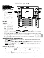
Reviews: