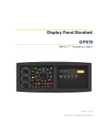
background image

SERVICE MANUAL

NTSC

ATSC

ready monitor

D8MW

Chassis

PA

No. 0239

UT42X902 / D8MW
UT42V702 / D8MW

Remote controls:

UT42X902 -  P#: HL02561 (CLU-4981S)

UT42V702 - P#: HL02562 (CLU-4982S)

SERVICE MANUAL REVISION HISTORY INFORMATION

DATE

REVISION #

REASON

Oct. 03, 2008

 SM00001

FIRST ISSUE OF MANUAL

SPECIFICATIONS AND PARTS ARE SUBJECT TO CHANGE FOR IMPROVEMENT

LCD DISPLAY PANEL

OCTOBER 2008

HIMEX MANUFACTURING DIVISION

Summary of Contents for UT42V702/D8MW

Page 1: ...e controls UT42X902 P HL02561 CLU 4981S UT42V702 P HL02562 CLU 4982S SERVICE MANUAL REVISION HISTORY INFORMATION DATE REVISION REASON Oct 03 2008 SM00001 FIRST ISSUE OF MANUAL SPECIFICATIONS AND PARTS ARE SUBJECT TO CHANGE FOR IMPROVEMENT LCD DISPLAY PANEL OCTOBER 2008 HIMEX MANUFACTURING DIVISION ...

Page 2: ...hat contained in the operating instructions unless you are qualified to do so Before servicing this chassis it is important that the service technician read the IMPORTANT SAFETY INSTRUCTIONS in this service manual SAFETY NOTICE USE ISOLATION TRANSFORMER WHEN SERVICING Components having special safety characteristics are identified by a on the schematics and on the parts list in this service data a...

Page 3: ... removed from the 120V AC 60Hz source place a jumper across Line 1 and Line 2 of the three plug prongs do not connect with the third prong which is physical ground Using an insulation tester DC500V connect one of its leads to the AC plug jumper and touch with the other lead each exposed metal part antennas screwheads metal overlays control shafts etc particularly any exposed metal part having a re...

Page 4: ...1 Follow the general caution recommendations from Safety precautions section 2 If necessary to replace Panel module this work must be started after the panel module and the AC DC Power supply becomes sufficiently cool 3 Special care must be taken with the display area to avoid damaging its surface 4 The Panel Module shall not be touched with bare hands to protect its surface from stains 5 It is re...

Page 5: ...ound strap to any heatsink in this instrument Electrostatically Sensitive ES Devices Some semiconductor solid state devices can be damaged easily by static electricity Such components commonly are called Electrostatically Sensitive ES Devices Examples of typical ES devices are integrated circuits and some field effect transistors and semiconductor chip components The following techniques should be...

Page 6: ... used to remove and replace the IC When working with boards using the familiar round hole use the standard technique as outlined in paragraphs 5 and 6 above Removal 1 Desolder and straighten each IC lead in one operation by gently prying up on the lead with the soldering iron tip as the solder melts 2 Draw away the melted solder with an anti static suctiontype solder removal device or with solder ...

Page 7: ...Use this technique only on IC connections 1 Carefully remove the damaged copper pattern with a sharp knife Remove only as much copper as absolutely necessary 2 Carefully scratch away the solder resist and acrylic coating if used from the end of the remaining copper pattern Install jumper wire and solder 3 Bend a small U in one end of a small gauge jumper wire and carefully crimp it around the IC p...

Page 8: ...oval Chip Component Installation 1 Put a small amount of solder on the board soldering pads 2 Hold the chip component against the soldering pads with tweezers or with a miniature alligator clip and apply heat to the pad area with a 30 watt iron until solder flows Do not apply heat for more than 3 seconds How to Replace Flat lC Required Tools Soldering iron iron wire or small awl De solder braids M...

Page 9: ...se remove previous solder as much as possible from the soldering point When soldering please perfectly melt the lead free solder to mix well with the previous solder 3 Soldering iron for lead free solder Melting point of lead free solder is higher than solder containing lead Use of a soldering tool with temperature control and with much thermal capacitance is recommended Recommended temperature co...

Page 10: ... of the FCC Rules Operation is subject to the following two conditions 1 This device may not cause harmful interference and 2 This device must accept any interference received including interference that may cause undesired operation Modifications The FCC requires the user to be notified that any changes or modifications made to this device that are not expressly approved by Hitachi Home Electroni...

Page 11: ...ing stand 18 0 kg Including stand 20 9 kg No Model Name Indicated Value Chassis Max Rating W A 1 UT42X902 243 2 3 D8MW 2 UT42V702 243 2 3 D8MW POWER RATINGS 19 12 16 502 40 13 16 1036 2 36 3 4 934 19 11 16 500 28 11 16 728 26 11 16 678 1 15 16 50 16 5 16 413 7 7 7 8 200 20 3 4 526 8 12 3 16 310 1 9 16 39 9 Max 5 3 8 136 1 3 8 35 0 Min CIRCUIT PROTECTION CAUTION It is very important to replace the ...

Page 12: ...ing feature SPECIFICATIONS SPECIFICATION UT42X902 UT42V702 Panel Display dimensions Approx 42 inches measured diagonal 36 3 4 H x 20 3 4 V in Resolution 1920 H x 1080 V pixels Ambient conditions Temperature Operating 5ºC to 35ºC Storage 0ºC to 40ºC Relative humidity Operating 20 to 80 Storage 20 to 90 non condensing Power supply AC120V 60Hz Audio output speaker 6W 6W HDMI input Input terminals HDM...

Page 13: ...le Power On Connect the plug into the wall socket after all other connections are completed CAUTION Ensure that both ends of the power cord are easily accessible The Main Power Switch is factory set to On activated therefore after you connect the plug into the wall socket the color of the indicating lamp must turn Green and the Illumination Lamp turns Blue The image will display on screen Once the...

Page 14: ...e Up Ź button Volume Down Ż button Input Select OK button Menu Exit button Power Cord Socket 3 HDMI Input Terminal Please refer to the owner s guide for detailed information regarding the connections 3 1 4 2 Main Power switch Service use only RS232C 0 PC RGB DVI Analog Audio Input Terminal PC Connection Terminal D sub 15 Pin Reset button 0 Control panel located on the bottom MENU EXIT VOL INPUT OK...

Page 15: ...ROM renew procedure 16 2 3 Memory Initialize affected adjustments 16 3 Video Adjustment 3 1 RGB amplitude adjustment PC D SUB input 16 3 2 NTSC Composite video adjustment 17 4 Video Color Temperature adjustment 4 1 Video Color Temperature adjustment Cool 17 4 2 Video Color Temperature adjustment Normal 18 4 3 Video Color Temperature adjustment Warm 19 5 Another procedure to set to factory shipping...

Page 16: ...e the master power button b Keep pressing the menu key until the Service Menu appears on screen release menu key 2 To exit the Service Mode press MENU key of the remote control or the UT monitor the user menu OSD will appear The next picture shows the Service Mode OSD for the 42 models example 1 2 Changing data and selecting adjustment codes When the UT monitor is in the Service Mode use the remot...

Page 17: ...item no 630 to data value 6 2 2 EEPROM RENEW Procedure There are two methods FIRST METHOD 1 Enter Service Mode by the procedure in section 1 1 2 Change the data value of the adjustment item no 659 from 0 to 1 3 Push the OK button in the remote control The picture will disappear indicating that the initialization of the EEPROM is started 4 About 2 seconds later the initialization will finish and th...

Page 18: ... 750 0 mV which is 105 100 of the standard signal is equal to 714 3 mV The next graphics show the white raster pattern and the waveform of the signal All white raster pattern White signal waveform Adjustment Procedure 1 Enter the Service Mode Menu by following the procedure in section 1 1 2 Input the NTSC composite signal to the UT Monitor 3 Select the no 658 adjustment item in the Service Mode Me...

Page 19: ...el 90 2 Picture settings Factory setting Check that the mode is set as the factory shipping conditions Picture mode Dynamic 3 The color analyzer CA 210 should be verified by a spectrum radiation brightness meter such as the CS 1000 or standard LCD 4 Set aspect to full mode 5 Set the color analyzer CA 210 at the center of the pan el Adjustment procedures 1 Enter the Service mode by following the pr...

Page 20: ...w values NOTE At least one of the parameters should remain in the initial value REMARKS 1 Color temperature should be adjusted under the condi tion in which the screen is the brightest thus the initial value of adjustment is set at its maximum 2 Beware there is RESET in each of picture mode 3 When the adjustment items no 6 7 or 8 are selected the color temperature of the picture changes to warm mo...

Page 21: ...e Cool Back Light 20 Deep Color Off Contrast Mode Dynamic 3D Color Management On Black Enhancement Middle DNR Middle MPEG NR Low Cross Color NR Low Game Mode Off Film Mode Smooth2 3D Comb Filter Low RGB Input Composite only Color Temp Adjus Off Amplitude Red 0 Green 0 Blue 0 Cut off Red 0 Green 0 Blue 0 Picture RGB Contrast 31 Brightness 0 Color 0 Tint 0 Color Temperature Normal Color Temp Adjust ...

Page 22: ...erfect Volume Off Speakers On Function System Grayed out HDMI Control Auto Input Change Off System Standby None AV Center Control Off Setup HDMI Video Power Save Off RGB Input RGB Grayed out Color System Auto Grayed out Setup RGB Auto Adjust Horizontal Position 0 Vertical Position 0 Horizontal Clock 0 Clock Phase 0 Frequency Display On WXGA Mode Off RGB Input RGB Language English US ...

Page 23: ...D8MW TABLE OF CONTENTS 22 Instruction in software renewal After software version up set the following lists for reference Page Left Blank ...

Page 24: ...D8MW TABLE OF CONTENTS 23 Page Left Blank ...

Page 25: ...D8MW TABLE OF CONTENTS 24 Page Left Blank ...

Page 26: ...D8MW TABLE OF CONTENTS 25 Page Left Blank ...

Page 27: ...D8MW TABLE OF CONTENTS 26 Page Left Blank ...

Page 28: ...D8MW TABLE OF CONTENTS 27 Page Left Blank ...

Page 29: ... set turned on can activate the mode 1 Set the service adjustment mode 2 Change No 646 from 0 to 1 After a few second appear the burn in picture 3 To escape from this mode change No 646 from 1 to 0 At first please confirm whether you put a connector cable again and a phenomenon comes out no picture no sound LED is not light Is the voltage of pin 5 5 4V of CNPS power supply unit normal It is troubl...

Page 30: ...e change No Go to 1 Yes It is trouble of Main PWB or Terminal PWB Picture trouble Go to A Sound trouble Go to B No Yes After a few seconds it becomes a red lighting even if it turns on power Main PWB Inverter PWB PPO1 pin 10 CN2 pin 12 PPO1 pin 11 CN2 pin 14 Are these connected No It is trouble of Power supply unit Please change Or please check ELCD2 connector or EPS connector Yes It is trouble of...

Page 31: ...ght turn on No Yes Are the voltage of pin 1 4 12V of PDO1 Main PWB normal It is trouble of Main PWB Please change No Yes It is trouble of LCD panel module No Is there voltage of pin 9 of CNPS Power supplyunit It is trouble of Main PWB Please change Yes It is trouble of Inverter PWB ...

Page 32: ...bit B 8bit H V DE CLK at RH33 RH35 RH37 and RH39 of Main PWB It is trouble of IA01 of Main PWB Please change Are there signals R G B H V at CE06 CE08 and IW01 pin1 13 of Main PWB It is trouble of QE01 QE03 or IE01of Main PWB Please change Yes Yes No Yes It is trouble of EFFC connector Terminal PWB or PW01 of Main PWB No Are there signals TMDS at RH60 67 of Main PWB It is trouble of IH01 of Main PW...

Page 33: ...signal No Yes Yes No Yes Check the signal at the P301 of Terminal PWB Change speaker Has it been improved It is trouble of the speaker Change EISP cable Change Terminal PWB Has it been improved It is trouble of the Terminal PWB Change EFFC cable Has it been improved Yes It is trouble of the EFFC cable No Change Main PWB ...

Page 34: ...㪪㪧 㪥㪡㪬㪉㪍㪇㪋㪈 㪥㪡㪬㪉㪍㪇㪋㪈 㪥㪡㪬㪉㪍㪇㪋㪈 㪥㪡㪬㪉㪍㪇㪋㪈 㪠㪉㪪 㪩㪜㪪㪜㪫 㪛㪄㪘㪤㪧 㪛㪄㪘㪤㪧 㪛㪄㪘㪤㪧 㪛㪄㪘㪤㪧 㪫㪘㪪㪌㪎㪇㪍 㪫㪘㪪㪌㪎㪇㪍 㪫㪘㪪㪌㪎㪇㪍 㪫㪘㪪㪌㪎㪇㪍 㪧㪛㪮㪥 㪩㪜㪪㪜㪫 㪠㪉㪪 㪤㪬㪫㪜 㪤㪚㪣㪢 㪤㫀㫅㪧㫀㫅㪡㪸㪺㫂 㪤㫀㫅㪧㫀㫅㪡㪸㪺㫂 㪤㫀㫅㪧㫀㫅㪡㪸㪺㫂 㪤㫀㫅㪧㫀㫅㪡㪸㪺㫂 㪧㪚㩷㪘㫌㪻㫀㫆 㪘㫌㪻㫀㫆㩷㪪㪮㪆㪛㪼㫃㪸㫐 㪣㩷㫆㫌㫋 㪩㩷㫆㫌㫋 㪣㪧㪣㩷㪋㪉㪭㩷㪝㪟㪛㩿㪈㪉㪇㪀 㪣㪧㪣㩷㪋㪉㪭㩷㪝㪟㪛㩿㪈㪉㪇㪀 㪣㪧㪣㩷㪋㪉㪭㩷㪝㪟㪛㩿㪈㪉㪇㪀 㪣㪧㪣㩷㪋㪉㪭㩷㪝㪟㪛㩿㪈㪉㪇㪀 㪂㪈㪉㪭 㪣㪭㪛㪪㪶㪪㪜㪣 㪣㪭㪛㪪 㪣㪭㪛㪪 㪣㪭㪛㪪 㪣㪭㪛㪪 㪉㪋㪭 㪙㪣㩷㪦㪥 㪙㪩㪫 㪙㪣㪶㪝㪘㪠㪣 㪚㪫㪪㪃㩷㪩㪫㪪 㪫㫏㪃㩷㪩㫏 㪠㪉㪪㩿㪛㪼㫃㪸㫐㩷㫆㫌㫋㪀 㪟㪧㪶㪛㪜㪫 㪟㪧㪶㪤㪬㪫㪜 㪫㫏㪃㩷㪩㫏㪃㩷㪚㪣㪢㪃㩷㪜㪥㪃㩷㪞㪶㪟...

Page 35: ... 8 9 10 G1 G2 CN1 PH 14H 1 2 3 4 5 6 7 8 9 10 11 12 13 14 G1 G2 CN2 PH 12H 1 2 3 4 5 6 7 8 9 10 11 12 G1 G2 Main P W B JA30711 2 POWER P W B Terminal P W B JA30721 2 3 A B Filter P W B Control P W B IR PWR_SW P W B Speaker Lout N Lout P Rout N Rout P 24V POWER 1 GND STB5V POWER OFF GND AC CLOCK BRT BL ON ON OFF 24V 24V AC CLOCK BRT BL ON ON OFF 24V STB5V POWER OFF GND GND POWER 1 FANLOCK FANVCC GN...

Page 36: ...XOG QRW WRXFK WKH PDLQ 3 V VKLHOGLQJ FDVH 㩷 㶎㪋㩷7DNH ORRVHQLQJ RI WKH 63 ZLUH VR WKDW DORQJ WKH JXLGH RI H HO DVV R WKH VW OLQJ VR WKDW WKH ZLUH VKRXOG QRW WRXFK WKH VZLWFK 㩷 㶎㪌㩷 R WKH VW OLQJ VR WKDW WKH 63 ZLUH DORQJ WKH JXLGH RI H HO DVV 㩷 㩷 1LWWR W DSH 1R PP PP㩷 㩷 1LWWR W DSH 1R PP PP㩷 㩷 0 6 1 6 7 3 㩷 㩷 0 6 1 6 7 3 㩷 㩷 1LWWR W DSH 1R PP PP㩷 㶎㪈 㶎㪊 㶎㪉 㶎㪌 㩷 1LWWR W DSH 1R PP PP㩷 㶎㪌 㶎㪋㩷 㩷 1LWWR W D...

Page 37: ...D8MW TABLE OF CONTENTS 36 䇼Pre operation䇽㩷 㪈㩷 Set the ferrite core NECN1 to ECN1 NECN1 MAG K5BFP 40X2X12 K P GX00821 WN03 Nitto tape No 5 W 20mm L 70mm ECN1 Wiring Diagram page 2 6 ...

Page 38: ... 㪥㪇㪇㪈㩷 㪜㪤㪫㪉㩷 㪓㪄㪄㩷 㪤㪸㫀㫅㩷 㪧㪮㪙㩷 㫊㫀㪻㪼㩷 㪫㪼㫉㫄㫀㫅㪸㫃㩷 㪧㪮㪙㩷 㫊㫀㪻㪼㩷 㪄㪄㪕 ޣ surface ޤ Ferrite core is 1set by 2pcs 㪌㫄㫄㫧㪈㫄㫄 㩷 WN01 Nitto tape No 5 W 20mm L 70mm 㪓㪄㪄㪫㪼㫉㫄㫀㫅㪸㫃㩷 㪧㪮㪙㩷 㫊㫀㪻㪼㩷 㪤㪸㫀㫅㩷 㪧㪮㪙㩷 㫊㫀㪻㪼㪄㪄㪕㩷 ޣ reverse ޤ ޣ side ޤ 㪓㪄㪄㩷 㪤㪸㫀㫅㩷 㪧㪮㪙㩷 㫊㫀㪻㪼 㪫㪼㫉㫄㫀㫅㪸㫃㩷 㪧㪮㪙㩷 㫊㫀㪻㪼㩷 㪄㪄㪕㩷 Wiring Diagram page 3 6 ...

Page 39: ...AL SLD TAPE P MD20801 㩷 ECN1 㪋㪅㩷 㩷 㪟㫆㫎㩷 㫋㫆㩷 㫊㫋㫐㫃㫀㫅㪾㩷 㵰㪜㪠㪪㪧㵱㩷 㫎㫀㫉㪼㩷 㫋㪿㪸㫋㩷 㪪㪧㪣㩷 㫊㫀㪻㪼㪅㩷 㩷 㩷 㩷 㩷 052 333 dose not touch the NECN1 Separate 1mm or more 333 1mm or more 333 Black tape EISP wire Guide of bezel 3mm or less Speaker L NECN1 WN04 Nitto tape No 5 W 9mm L 30mm N001 Wiring Diagram page 4 6 ...

Page 40: ... 㪍How to set the ferrite core NSPK NSPK2 to EISP 㩷 㪜㪠㪪㪧㩷 㪌㪇㫄㫄㫧㪌㫄㫄 㪉㪇㫄㫄㫧㪌㫄㫄 Main PWB side LED PWB side NELS MAG K5CRC12X15X7 MB2 P GX00738 1 turn SP R side Main PWB side Terminal PWB side Binding tape Binding tape NSPK2 MAG K5CRC12X15X7 MB2 P GX00738 1 turn SP L side NSPK MAG K5CRC12X15X7 MB2 P GX00738 1 turn ...

Page 41: ... 6 㪎㩷 Paste 327 so that ECN1 ECN2 should not float 0 0 327 Nitto tape No 5 W 20mm L 100mm㩷 㪏㩷 How to set the ferrite core NEPU㩷 to EPU 20mm 25mm 78mm or more NEPU MAGK5CRC16X28X9 M2G2 P GX00732 Put on the core with fit ኒ ߐߖࠆ NEPU SK binder P 3763751 ...

Page 42: ...D8MW TABLE OF CONTENTS Final assembly guide 41 1 9 ...

Page 43: ...D8MW TABLE OF CONTENTS Final assembly guide 42 2 9 ...

Page 44: ...D8MW TABLE OF CONTENTS Final assembly guide 43 3 9 ...

Page 45: ...D8MW TABLE OF CONTENTS Final assembly guide 44 4 9 ...

Page 46: ...D8MW TABLE OF CONTENTS Final assembly guide 45 5 9 ...

Page 47: ...D8MW TABLE OF CONTENTS Final assembly guide 46 6 9 ...

Page 48: ...D8MW TABLE OF CONTENTS Final assembly guide 47 7 9 ...

Page 49: ...D8MW TABLE OF CONTENTS Final assembly guide 48 8 9 ...

Page 50: ...D8MW TABLE OF CONTENTS Final assembly guide 49 9 9 ...

Page 51: ...o signal and for the audio a 1Vp p 1kHz audio signal was used PC video signal white icon numbers example HDMI video signal black icon numbers example PC signal green color CE12 page 62 PC signal blue color CE13 page 62 PC signal red color CE14 page 62 PC signal horizontal drive RE49 page 62 PC signal vertical drive RE50 page 62 PC signal green color CE06 page 62 ...

Page 52: ...continued PC signal blue color CE07 page 62 PC signal red color CE08 page 62 PC signal sub vertical drive IW01 pin 1 page 72 PC signal sub horiz drive IW01 pin 13 page 72 HDMI signal HDMI CLK RH33 page 63 HDMI signal HDMI CB RH35 page 63 ...

Page 53: ...W TABLE OF CONTENTS 52 WAVEFORMS continued HDMI signal HDMI Y RH37 page 63 HDMI signal HDMI CB RH35 page 63 HDMI signal RX RH60 RH67 page 63 Audio signal Input R225 page 74 Audio signal output P301 page 75 ...

Page 54: ...10 8 10 8 10 8 0 0 5 5 55 0 0 5 3 0 IR PWR_SW P701 0 3 2 0 5 2 0 0 3 1 5 2 5 3 0 2 POWER CNPS 23 8 23 8 0 0 5 3 0 3 3 2 3 3 3 3 0 2 CNPP1 23 8 23 8 23 8 23 8 23 8 0 0 0 0 0 3 2 3 3 0 2 0 2 CNPP2 23 8 23 8 23 8 23 8 23 8 0 0 0 0 0 3 2 3 3 DC VOLTAGES To allow a quick check the next table shows the direct current voltages of the most accesible connector terminals in the LCD UT monitor ...

Page 55: ... Flash Memory EEPROM DDC DDC EEPROM EEPROM TxRx Bus SW I2S I2S LVTTL LVDS I2S I2S I2C Analog RGB L R 24V STB 5V CEC UART FC Bus 232C Tranciever TMDS Audio DSP I2S LVDS FAN VCC Key Switch LED iR LVDS Control etc Audio ADC RS232C iR Out Audio AMP Audio In Mini Jack Analog RGB In HDMI In Sub MPU Renesas M16C64 DDR2 Memory DDR2 Memory DDR2 Memory DDR Memory HDMI Rx Silicon Image SiI9125 FC8 Scaler IC ...

Page 56: ...09 1C 012 1D 5 6V 003 G4 004 2A 008 4A 009 1C 011 1B 012 1A 015 2A 016 1A 020 2B STB 5V 012 4E 012 8E 013 5C 014 2B 014 2D 015 2A 020 2C 020 5D D 3 3V 003 C6 003 G4 004 2E 005 1C 006 1A 009 1A 011 1A 016 1A 017 1A 017 6C 019 3E 019 4A 019 4D 019 6A 019 6D 020 4E PWR_OFF 005 1E 012 1E 020 4C 020 4D 020 7D STB 3 3V 012 1A 013 5B 014 2B PON_TCON 012 1D POWER2TD 012 1D 015 2B 016 1B 020 2C PON_3 3V 01...

Page 57: ...V 002 5D C6 004 2E 005 1C 006 1A 009 1A 011 1A 016 1A 017 1A 017 6C 019 3E 019 4A 019 4D 019 6A 019 6D 020 4E D 3 3V 002 5D G4 004 2E 005 1C 006 1A 009 1A 011 1A 016 1A 017 1A 017 6C 019 3E 019 4A 019 4D 019 6A 019 6D 020 4E AMP_PWR 002 5E 020 2B FANVCC 002 8D Tcon 12V 002 8C 019 6C FAN_ALRM 009 1B 5 6V 002 5C 004 2A 008 4A 009 1C 011 1B 012 1A 015 2A 016 1A 020 2B OVDET_N 012 1E AMP_PWR D 3 3V 5 ...

Page 58: ...D1 RG19 300k 1 1 2 RG11 47k 1 2 RG22 300k 1 1 2 RG21 7 5k 1 1 2 RG20 300k 1 1 2 RG18 7 5k 1 1 2 RG12 15k 1 1 2 RG10 10k 1 2 RG14 10k 1 1 2 RG17 300k 1 1 2 RG13 0 1 2 RG01 2010 0 1 2 3 4 5 6 7 8 RG02 2010 0 1 2 3 4 5 6 7 8 D 3 3V 002 5D 003 C6 003 G4 005 1C 006 1A 009 1A 011 1A 016 1A 017 1A 017 6C 019 3E 019 4A 019 4D 019 6A 019 6D 020 4E DDR_VCC2 007 1C DDR_VCC1 007 1A GEN 1 8V 005 1B 007 1E 009 ...

Page 59: ...RPLL_DGND C25 RPLL_18 A26 RPLL_AGND A26 A25 RPLL_AGND A25 B26 XTAL C26 TCLK AD9 RESETn AF13 EXT_OSD_CLK AC13 EXT_OSD_HS AD13 EXT_OSD_VS AD12 AVS_IN_WORD_SEL AF14 AVS_IN_SCL AC12 AVS_IN_DATA W23 OCM_INT1 Y24 OCM_INT2 W26 OCM_UDO_0 W25 OCM_UDI_0 B2 OCM_UDO_1 B3 OCM_UDI_1 AB24 IR0 V24 PWM0 U23 PWM1 U24 PWM2 W24 OCM_TIMER1 AA23 MSTR0_SDA AA24 MSTR0_SCL A2 MSTR1_SDA A3 MSTR1_SCL AB25 MSTR2_SDA AB26 MST...

Page 60: ...5 A4 A3 A2 A1 A0 CE Vss 27 OE DQ0 DQ8 DQ1 DQ9 DQ2 DQ10 DQ3 DQ11 Vcc 37 DQ4 DQ12 DQ5 DQ13 DQ6 DQ14 DQ7 DQ15 Vss 46 NC 47 A16 IA01 FLI8538 LF BE AF15 OCMADDR_21 AE15 OCMADDR_20 AD15 OCMADDR_19 AC15 OCMADDR_18 AF16 OCMADDR_17 AE16 OCMADDR_16 AD16 OCMADDR_15 AF17 OCMADDR_14 AE17 OCMADDR_13 AD17 OCMADDR_12 AC17 OCMADDR_11 AF18 OCMADDR_10 AE18 OCMADDR_9 AD18 OCMADDR_8 AF19 OCMADDR_7 AE19 OCMADDR_6 AD19 ...

Page 61: ...05 0 1 16 1 2 CC22 1005 0 1 16 1 2 CC33 1005 0 1 16 1 2 CC24 1005 0 1 16 1 2 CC27 1005 0 1 16 1 2 CC26 1005 0 1 16 1 2 CC44 1005 470p 1 2 CC29 1005 0 1 16 1 2 CC31 1005 0 1 16 1 2 CC45 1005 470p 1 2 CC32 1005 0 1 16 1 2 CC42 1005 470p 1 2 CC35 1005 0 1 16 1 2 CC36 1005 470p 1 2 CC37 1005 0 1 16 1 2 CC25 2125 22 6 3 1 2 CC23 2125 22 6 3 1 2 CC04 2125 22 6 3 1 2 CC03 2125 22 6 3 1 2 CC01 2125 22 6 3...

Page 62: ...O F26 CH1N_LV_O F25 CH1P_LV_O F24 CH2N_LV_O F23 CH2P_LV_O G24 CH3N_LV_O G23 CH3P_LV_O N26 CH4N_LV_O N25 CH4P_LV_O G26 CLKN_LV_O G25 CLKP_LV_O R23 PD_10BIT_EGRN1 T26 PD_10BIT_EGRN0 R25 PD_10BIT_EBLU1 R24 PD_10BIT_EBLU0 T25 PD_10BIT_ERED1 T24 PD_10BIT_ERED0 P24 DCLK R26 DVS P25 DHS P26 DEN M24 N C M24 U25 PPWR U26 PBIAS GND1 GND1 GND1 GND1 GND1 GND1 2518 LD02 47 1 2 2518 LD01 47 1 2 RD20 1 0k 1 2 RD...

Page 63: ... AD7 ADC_3 3_SC AB4 ADC_1 8 AB4 AC4 ADC_1 8 AC4 AC5 ADC_1 8 AC5 AB3 AGND_ADC AB3 AC3 AGND_ADC AC3 AD2 AGND_ADC AD2 AC6 AGND_ADC AC6 AC8 AGND_ADC AC8 AD8 AGND_ADC AD8 AE3 AGND_ADC AE3 AE6 AGND_ADC AE6 AE9 AGND_ADC AE9 AA2 DGND_ADC AA2 AA3 DGND_ADC AA3 AA4 DGND_ADC AA4 GND1 GND1 GND1 GND1 GND1 GND1 GND1 GND1 GND1 GND1 GND1 GND1 GND1 GND1 GND1 GND1 GND1 2518 LE02 47 1 2 2518 LE01 22 1 2 TPE01 1 TPE02...

Page 64: ...Q14 Q13 Q12 CGND 142 CVCC18 143 Q11 G1 G2 G3 G4 G5 G6 G7 G8 G9 G10 G11 G12 G13 G14 G15 G16 G17 G18 G19 G20 G21 G22 G23 G24 G25 RH50 470k 1 2 RH16 1 0M 1 2 RH28 4 7k 1 2 RH01 47 1 2 RH48 33 1 2 RH25 33 1 2 RH26 33 1 2 RH02 47 1 2 RH46 10k 1 2 RH04 100 1 2 RH08 1 0k 1 2 RH47 10k 1 2 RH29 10k 1 2 RH15 47k 1 2 RH14 47k 1 2 RH53 470k 1 2 RH52 470k 1 2 RH51 470k 1 2 RH30 10k 1 2 RH31 4 7k 1 2 RH03 0 1 2...

Page 65: ...RM16 0 1 2 RM13 0 1 2 RM64 10k 1 2 RM51 4 7k 1 2 RM87 47k 1 2 RM72 100k 1 2 RM86 680k 1 2 RM59 4 7k 1 2 RM53 10k 1 2 RM71 27k 1 1 2 RM81 0 1 2 RM07 0 1 2 RM05 100 1 2 RM32 10k 1 2 RM37 1 0k 1 2 RM17 0 1 2 RM97 10k 1 2 RM10 0 1 2 RM36 1 0k 1 2 RM76 100 1 2 RM20 2010 100k 1 2 5 6 3 4 7 8 RM09 2010 10k 1 2 3 4 5 6 7 8 RM06 2010 10k 1 2 3 4 5 6 7 8 RM08 2010 100 1 2 3 4 5 6 7 8 RM43 2010 1 0k 3 4 5 6 ...

Page 66: ...16 1 2 CV01 1005 0 01 25 1 2 STB 5V 002 7A 012 4E 012 8E 014 2B 014 2D 015 2A 020 2C 020 5D PWRSW_N 012 1E 020 4D CV11 1005 0 1 16 1 2 LEDG 012 8B GND1 PoWER1 012 1E RV03 4 7k 1 2 LEDo 012 8B PV01 501568 10H 1 2 3 4 5 6 7 8 9 10 G1 G2 CV10 1005 0 1 16 1 2 CV05 1005 0 1 16 1 2 CV12 1005 0 1 16 1 2 CV03 1005 0 01 25 1 2 RV01 1 0k 1 2 STB 3 3V 002 7B 012 1A 014 2B LEDR 012 8B CV13 1005 470p 1 2 CV14 ...

Page 67: ...3 QS01 2SC5383 T111 1F 1 2 3 RS23 10k 1 2 RS28 47k 1 2 RS32 1 0k 1 2 RS20 10k 1 2 RS22 10k 1 2 RS06 100 1 2 RS18 1 0k 1 2 RS38 0 1 2 RS03 0 1 2 RS21 10k 1 2 RS29 47k 1 2 RS02 0 1 2 RS12 100 1 2 RS26 22k 1 2 RS11 100 1 2 RS33 10k 1 2 RS16 1 0k 1 2 RS15 1 0k 1 2 RS17 1 0k 1 2 RS27 22k 1 2 RS04 0 1 2 RS05 100 1 2 RS13 470 1 2 RS14 470 1 2 RS01 0 1 2 RS37 100k 1 2 RS36 10k 1 2 RS35 10k 1 2 RS34 10k 1 ...

Page 68: ...17 10k 1 2 RR29 68k 1 2 6331 RR02 22 1 2 RR15 10k 1 2 RR34 270k 1 2 RR09 1 0k 1 2 RR20 10k 1 2 RR21 10k 1 2 RR31 82k 1 2 RR33 100k 1 2 RR19 10k 1 2 RR27 47k 1 2 RR13 5 6k 1 2 RR10 1 8k 1 2 RR24 0 1 2 RR28 56k 1 2 RR32 100 1 2 RR12 5 6k 1 2 RR26 47k 1 2 RR30 68k 1 1 2 RR03 2010 0 1 2 3 4 5 6 7 8 IR_SW 012 8B 5 6V 002 5C 003 G4 004 2A 008 4A 009 1C 011 1B 012 1A 016 1A 020 2B STB 5V 002 7A 012 4E 01...

Page 69: ...ECLKN D9 RXECLKP A9 RXiNEDN B9 RXiNEDP A8 RXiNEEN B8 RXiNEEP A14 RXiNoAN B14 RXiNoAP C14 RXiNoBN D14 RXiNoBP A13 RXiNoCN B13 RXiNoCP C13 RXoCLKN D13 RXoCLKP A12 RXiNoDN B12 RXiNoDP C12 RXiNoEN D12 RXiNoEP D8 LVDSRXVCC D8 E9 LVDSRXVCC E9 D11 LVDSRXVCC D11 E13 LVDSRXVCC E13 E10 LVDSRXVSS E10 E11 LVDSRXVSS E11 E14 LVDSRXVSS E14 E8 LVDSRXVDDD E8 E12 LVDSRXVDDD E12 C8 LVDSRXGNDD C8 C11 LVDSRXGNDD C11 R...

Page 70: ... 1 2 CJ38 4 7 6 3 1 2 CJ36 4 7 6 3 1 2 FC 1 05V CJ32 4 7 6 3 1 2 IJ01 FC8 AA12 VDD AA12 B33 VDD B33 G29 VDD G29 P12 VDD P12 V22 VDD V22 AA22 VDD AA22 M12 VDD M12 P22 VDD P22 W12 VDD W12 AB12 VDD AB12 C33 VDD C33 M14 VDD M14 R12 VDD R12 W22 VDD W22 AB14 VDD AB14 D31 VDD D31 M16 VDD M16 R22 VDD R22 Y12 VDD Y12 AB16 VDD AB16 D32 VDD D32 M18 VDD M18 T12 VDD T12 Y22 VDD Y22 AB18 VDD AB18 M20 VDD M20 T2...

Page 71: ...GND1 GND1 RK42 22 1 2 IJ01 FC8 AB33 VCCQ18 AB33 AJ19 VCCQ18 AJ19 AL19 VCCQ18 AL19 L29 VCCQ18 L29 Y29 VCCQ18 Y29 AC29 VCCQ18 AC29 AJ21 VCCQ18 AJ21 AL20 VCCQ18 AL20 AN23 VCCQ18 AN23 L31 VCCQ18 L31 Y30 VCCQ18 Y30 AD31 VCCQ18 AD31 AJ22 VCCQ18 AJ22 AL22 VCCQ18 AL22 AN27 VCCQ18 AN27 N31 VCCQ18 N31 Y31 VCCQ18 Y31 AD33 VCCQ18 AD33 AJ26 VCCQ18 AJ26 AL26 VCCQ18 AL26 D33 VCCQ18 D33 P29 VCCQ18 P29 Y33 VCCQ18 ...

Page 72: ...G3 G4 G5 G6 G7 G8 G9 G10 CL02 1005 0 01 25 1 2 RL45 2010 0 1 2 3 4 5 6 7 8 RL01 0 1 2 3 4 5 6 7 8 RL23 0 1 2 CL04 0 1 16 1005 1 2 CL05 0 1 16 1005 1 2 RL44 2010 0 1 2 3 4 5 6 7 8 CL17 0 1 16 1005 1 2 RL51 2010 0 1 2 3 4 5 6 7 8 GND1 CL11 0 1 16 1005 1 2 CL31 0 1 16 1005 1 2 CL13 0 1 16 1005 1 2 Tcon 12V 002 8C 003 G5 Tcon 12V RAiKo_N 005 7D LVDS_SEL 009 1B RL53 10k 1 2 GND1 RL26 10k 1 2 IJ01 FC8 A...

Page 73: ...FF 002 8B 005 1E 012 1E 4C 7D PC_VD 009 1E Dsub_H 2D STB 5V 002 7A 012 4E 012 8E 013 5C 014 2B 014 2D 015 2A 2C PWRSW_N 012 1E 013 5D HP_MUTE 008 5E HP_MUTN 2C PWR_OFF 002 8B 005 1E 012 1E 4D 7D CW09 1005 100p C 1 2 CW08 1005 100p C 1 2 CW04 1005 470p 1 2 CW10 1005 100p C 1 2 AUD_RSTn 6C STB 5V 002 7A 012 4E 012 8E 013 5C 014 2B 014 2D 015 2A 5D AMP_PWR 002 5E 003 G6 PC_Blue 009 1D DLY_LRCK 005 7E...

Page 74: ...2 6C HP_DET J6 HDM_MCLK 003 2D HP_MUTN 004 2C 004 6C TxD J4 RxD J3 POWER2TD 002 6D 003 2B CTS J3 DTR J4 RTS J3 ADC_SCLK 002 5B ADC_WS 002 5B IRo_term H6 J4 ADC_SD 002 5B DLY_SCLK_S 002 2E DLY_WS_S 002 2E R105 0 1 2 DLY_SD_S 002 2E DLY_SCLK_H 004 2C DLY_SD_H 004 2C R107 0 1 2 R106 0 1 2 R110 0 1 2 R108 0 1 2 DLY_WS_H 004 2C R109 0 1 2 AudioRSTn 002 2D 003 2B 004 2C AUD_SDA 002 2D 003 2C 004 4C MCLK...

Page 75: ... GND1 GND1 GND1 GND1 GND1 GND1 GND1 GND1 1608 L201 BLM18BD471SN1D 1 2 1608 L203 BLM18BD471SN1D 1 2 1608 L202 BLM18BD471SN1D 1 2 J201 LGY6502 0800 1 GND 2 L 3 R R220 470 1 1 2 R217 47 1 2 R204 10k 1 2 R219 10k 1 2 R222 10k 1 2 R214 47 1 2 R209 47 1 2 R208 47 1 2 R207 47 1 2 R224 100 1 2 R223 100 1 2 R203 47 1 2 R202 47 1 2 R228 30k 1 1 2 R210 0 1 2 R215 0 1 2 R211 0 1 2 R225 18k 1 1 2 R226 30k 1 1 ...

Page 76: ...AS5706PAPR OUT_B 1 PGND_B 2 PGND_B 3 OUT_A 4 OUT_A 5 PGND_A 6 PGND_A 7 PVCC_A 8 PVCC_A 9 AVDD AVSS PLL_FLTM PLL_FLTP VR_ANA DVDD 15 RESET PDN VREG_EN OSC_RES DVSS 20 MUTE LRCLK SCLK SDIN2 SDIN1 DVSS 26 VR_DIG SDA SCL HPSEL STEST TEST2 DVDD 33 MCLK BKND_ERR VALID HPL_PWM HPR_PWM SUB_PWM SUB_PWM PVCC_D 41 PVCC_D 42 PGND_D 43 PGND_D 44 OUT_D 45 OUT_D 46 PGND_C 47 PGND_C 48 OUT_C 49 OUT_C 50 PVCC_D 51...

Page 77: ...GND1 1608 L402 BLM18BD471SN1D 1 2 1608 L403 120 1 2 1608 L401 BLM18BD471SN1D 1 2 Q403 2SA1989 T111 1 1 2 3 Q402 2SD2704K 1 2 3 Q401 2SD2704K 1 2 3 R409 1 0k 1 2 R426 1 0k 1 2 R429 1 0k 1 2 R414 1 0k 1 2 R411 10k 1 2 R430 1 0k 1 2 R420 100 1 2 R410 10k 1 2 R413 0 1 2 R424 10k 1 2 R425 1 0k 1 2 R419 100 1 2 R422 100 1 2 R416 10k 1 2 R415 10k 1 2 R417 10k 1 2 R407 0 1 2 R401 510k 1 1 2 R402 82k 1 1 2...

Page 78: ...8 9 10 11 12 13 14 15 G1 G2 2125 X504 SC100JT 1 2 3 2125 X501 SC100JT 1 2 3 2125 X503 SC100JT 1 2 3 2125 X502 SC100JT 1 2 3 GND5 GND5 GND5 GND5 GND5 GND5 GND5 GND5 GND5 GND5 GND5 GND5 GND5 GND5 GND5 2518 L501 47 1 2 Q501 2SC5383 T111 1F 1 2 3 R501 0 1 2 R509 75 1 1 2 R516 100 1 2 R508 47k 1 2 R502 47k 1 2 R518 100 1 2 R511 75 1 1 2 R515 100 1 2 R507 47k 1 2 R505 2 2k 1 2 R519 47k 1 2 R517 10k 1 2 ...

Page 79: ... LED P602 501568 04H 1 2 3 4 G1 G2 P601 501568 06H 1 2 3 4 5 6 G1 G2 GND4 GND4 GND4 GND4 GND4 GND4 D602 SMLA12BC6T 1 B 2 D603 SMLA12BC6T 1 B 2 D601 SMLA12BC6T 1 B 2 Q603 2SC5383 T111 1F 1 2 3 Q602 2SC5383 T111 1F 1 2 3 Q601 2SC5383 T111 1F 1 2 3 R603 150 1 2 R601 150 1 2 R602 150 1 2 R605 2010 10k 1 2 3 4 5 6 7 8 R606 2010 47k 1 2 3 4 5 6 7 8 USRRST ADKEY1 ADKEY2 GND USRRST ADKEY1 ADKEY2 GND LEDB ...

Page 80: ...Vcc GND G1 G2 D701 SML 512UW 1 R 2 D702 SML 512MW 1 G 2 TP701 1 TP702 1 Q701 2SC5383 T111 1F 1 2 3 Q703 2SC5383 T111 1F 1 2 3 Q702 2SC5383 T111 1F 1 2 3 R705 0 1 2 R710 470 1 2 R703 0 1 2 R708 2 7k 1 2 2125 R702 0 1 2 R711 0 1 2 R701 100 1 2 R709 220 1 2 R706 2010 10k 1 2 3 4 5 6 7 8 R707 2010 47k 1 2 3 4 5 6 7 8 D703 SML 512WW 1 Y 2 R712 390 1 2 R732 10k 1 2 Q720 2SC5383 T111 1F 1 2 3 R733 47k 1 ...

Page 81: ...1 5 6 4 3 2 1 5 6 4 3 2 1 5 6 4 3 2 1 5 6 4 3 2 1 P801 501568 04H 1 2 3 4 G1 G2 GND3 GND3 GND3 GND3 R804 1 0k 1 2 R801 4 7k 1 2 R803 1 5k 1 2 R814 0 1 2 R802 2 7k 1 2 S806 KSS6N23CTJ 1 2 3 4 5 6 S805 KSS6N23CTJ 1 2 3 4 5 6 S804 KSS6N23CTJ 1 2 3 4 5 6 S803 KSS6N23CTJ 1 2 3 4 5 6 S802 KSS6N23CTJ 1 2 3 4 5 6 S801 KSS6N23CTJ 1 2 3 4 5 6 S807 KSS6N23CTJ 1 2 3 4 5 6 VOL_DOWN CH_UP INPUT EXIT CH_DOWN VOL...

Page 82: ...NOTICE of this service manual Don t degrade the safety of the receiver through improper servicing 28 FILTER BOARD 3 2 1 F G C9A4 CS 2200p 400 1 2 C9A3 CS 2200p 400 1 2 F G C9A1 LE 0 22 1 2 C9A2 LE 0 22 1 2 F9A1 6 3A250V 1 2 NF9A1 PPU1 VH 03V D 2NC 1 NC 3 G001 1 2 F G G003 1 2 G004 1 2 P9A1 AC INLET 1 L 2 N 3 FG E002 01Bin 12m L9A1A 30x30 1 1 3 3 4 4 2 2 12m L9A2A 30x30 1 1 3 3 4 4 2 2 16m L9A2C 32...

Page 83: ...D8MW TABLE OF CONTENTS PRINTED CIRCUIT BOARDS 82 page 1 5 Main board components side ...

Page 84: ...D8MW TABLE OF CONTENTS PRINTED CIRCUIT BOARDS 83 page 2 5 Main board solder side ...

Page 85: ...D8MW TABLE OF CONTENTS PRINTED CIRCUIT BOARDS 84 page 3 5 Terminal board Component side Terminal board Solder side ...

Page 86: ...8MW TABLE OF CONTENTS PRINTED CIRCUIT BOARDS 85 page 4 5 Control board Component side IR board Component side LED board Component side Control board Solder side IR board Solder side LED board Solder side ...

Page 87: ...D8MW TABLE OF CONTENTS PRINTED CIRCUIT BOARDS 86 page 5 5 Filter board Component side Filter board Solder side ...

Page 88: ...03973 SCRW M3M 6 25 SM 0 0 128 MC02283 UT SIGNAL GEL 15 15 T5 0 0 508 MJ04154 SCRW M3M 5X12X L 0 0 129 MC02281 UT SIGNAL GEL 12 5 T8 0 0 510 QX03751 D8J PLASTIC BAND 0 0 260 PC07421 D8M POWER BUTTON 0 0 512 MJ03557 SCRW T2B_4 16BD SWCH16A 0 0 514 ML04321 PLASTIC RIVETP4100B 0 0 CONNECTORS ECN1 EF29006 51P 0 5MM PITCH VLDS CABLE L 250MM 0 0 OWNER S ASSEMBLY ECN2 EF29141 41P 0 5MM PITCH LVDS CALBE L...

Page 89: ...4953 MAIN board under the metal UX34945 UT42X902 UX34946 UT42V702 Filter board JT25992 Power Supply Board HA02581 Inverter board S HP02671 PH BLC187 Power switch IR board part of UX34953 LED board at the front part of UX34953 Control panel board underneath part of UX34953 Right Speaker GM01868 Left Speaker GM01867 PANEL DD02671K ...

Page 90: ...PA NO 0239 MADE IN MEXICO ...

Reviews: