background image

Summary of Contents for MP-1802

Page 1: ......

Page 2: ...I I I 1 I F BASIC MASTER LEVEL 3 Minif loppy Disk Dr j_ve Unit Mp 3550 ano Minifloppy Disk Card Mp 1 B02 SERVICE MANUAL 1982 ...

Page 3: ...ications ln Part Names 5 Termj nal Connection Specif ication 6 Explanation of f Cs in Use 7 Circuit Explanation 8 Adj ustment Method 9 Minifloppy Disk Card Expansion Method 10 Servi ee Point s 11 Trouble Shooting 1 1 2 lr 5 21 2 5B O J 67 71 ...

Page 4: ...ted once Level 3 eonnector 2 MP 1BO2 The minifloppy disk card MP 1 802 is inserted in the expansion slot of the Level 3 I t is the LeveI 3 expansion interface card which enables conneetion with the MP 3550 UNIT 1 f rst unit and the MP 3550 UNIT 2 second unit FEATURES x MP _3550 1 Program recording and reading is aceomplished quickly and reliably 2 Data input output and correction can be executed s...

Page 5: ...may vary depending on the system diskette in use Refer to the system disk nanual f or details Environnent Conditions ftem Temp erat ur e Humidity Max Wet Bulb Temperature 0perati on 5oc 35oc 2or gof No dew at zgoc Non 0perati on 1ooc r5oc B1 8oi Tran spor tat i on 1ooc 5ooc B B0 Note During non operation or transportation the head protection sheet should be placed in eaeh drive afte the disk has b...

Page 6: ...tors 56 No of Diodes 75 Power AC 100V 50 60 Hz Power Consumption 55W Dimensions 27 0 W x 21 O H x 27 5 D cn We ight 9 o kg Accessories Dr ive belt Drive Capacity MP 3550 x 2 units lr drives I C Number 28 Transistor Number lr Diode Nunber 2 Power DC 5V Power Consumption 3W Dirnens ions 1 0 0 W x tr 5 jf x 23 5 D cm We ight 0 31 kg 4 ...

Page 7: ...4 l MP 3550 oRrvE 0 O R I V E I drive 1 drive 2 power switch I r o l l _ oFF power cord holder fan connector data POwer Ccrrc 2 MP 802 to MP 355OttNIT l l DB A C 8 I DB BP C B 3 edge conneetor to J eyel3 power lamp 5 ...

Page 8: ...n index hole is detected after diskette is rota ted 5 m0 Enables Drive 0 signal sending and receiving w h e n l L I 6 SIET1 Enables Drive 1 signal sending and receivi ns w h e n l L I 7 mffi Enables Dri ve 2 signal sending and receiving w h e n l L I 8 MOTOR ON Drive motor operates w h e n l L I 9 DI RECTI ON IN Control s head movement direction 10 STEP t Moves the head one track per pulse 11 i mT...

Page 9: ...rm restoration 16 mE1 Sel ects Side t head when tL t S ide 0 head when tH t 17 D RCLK Clock signal to divide data bit and clock bit from R EAD DAT A 1B 5v 5V power supply 19 T t 20 21 zz 23 2 1 J J 25 5v 26 DOUBLEDEN Becomes rHr when writing and recording of double density 27 GND GROUN D 2B 1 i 2g 30 31 1 33 3lr 35 36 37 7 ...

Page 10: ...Pin No Signa 1 Data Direction Level 3oInside E planation 38 39 lr0 1 2 lr3 lt lr5 lr6 7 J I l 8 GND lr9 50 rr fr Unused term i nal 8 ...

Page 11: ...ecomes rrLrr when the disk rotates n orma11y 7 n n T n LJII J GROUND B INDEX 0u tput tfLrr pulse when i ndex hole is detected after diskrs ro tatio n GND GRO UND 10 Sgi gCT O Enables drive 0 sig receive sendable when I t r r l 1 11 GND GRO UND 12 SEIEMl When rfLrr enable s send ing frecei ving of drive 1 13 GND GROUN D 4 t t 4 t GND GROUND t o MOTOR ON Drive motor oDerate s w h e n l fL l f 17 GND...

Page 12: ...E GATE When frLrr enable write 25 GND c GRO UND 26 TRACKOO Bec ome s frL rf when head is in track 00 position 27 cNl GROUND 2B WRITE PROTECT Beeomes lrLll when write protected disl is inserted 2g GND GROUND 30 READ DATA Read data s ig from the di sk 31 GND __ GROUND 32 SI DE T Seleet side t head when frLrtrside 0 heac when frHil 33 GND ___ GROUND 3lr tr rr unused terminal 10 ...

Page 13: ...f r eceiv ing ih rt l T I 7 tuotonoll Drive motor operate s when lL I 9 m Controls head movement direction 10 d m n n I H P V L J I L Mo ve s head one track per puls e 11 WRITE DATA Write data s ignal t o diskette 12 WRITE GATE _ J Writing is possible when rL r 13 TRACI OO Becomes rL I when head is in Track 00 Dos itio n 1 WRITE PROTECT Becomes rL I when write protected disk is inserted 15 mmIn F ...

Page 14: ...l Data Direction Level 3 lnside Explanation 1B 1g 20 21 22 23 2 25 26 DOUBLEDEN _ Becomes fH I with writing an d recording of double de ns ity 27 GND GROUND 2B 1 2g 30 31 32 33 3L 35 36 37 3B 39 0 l 1 l 2 lr3 lr 12 ...

Page 15: ...Pin No Si gn al Data Direction Level 3e Inside E planat i on lr5 r6 t 7 t 4 l J 8 GND 4 50 f r rt unused te rminal 13 ...

Page 16: ...ECT1 When tLt enables sending uceiving of Drive 1 signal 7 sj Em When rLr enables sending f receiving of Drive 2 signal B MOTOR ON Drive motor oDerate s when rL I 9 DI RECTIONIN Contr ols head movement direction 10 STEP Moves head one track per pulse 11 WRITE DATA Write data signal to diskette 12 WRITE GATE Writing is possible when rL I 13 TRACI O6 Bec omes r L I when head is in Track 00 positior ...

Page 17: ... planation 17 D RCLK Clock signal to divide data bit and clock bit from READ DATA 18 5v 1g t I 20 21 22 23 2 I I 25 5v 26 DOUBLEDEN Becomes rHr with writing and recording of double density 27 GND GROUND 28 I 2g 30 31 32 33 3lr 35 36 37 38 39 0 r1 15 ...

Page 18: ...Pin No Signa l Data Direction Inside UNI T 1 Explanat i on 2 r3 lr lr5 6 7 I I 8 GND 9 50 l l Un used term inal 16 ...

Page 19: ... o Sig nal Data Directi on Level 3 Inside E planation 1 Data bus 2 3 DO lr D1 5 D2 j 6 D3 7 D 8 D5 c __J 9 D6 ________ 10 D7 e 11 AO __ Addres s bus 12 A1 13 A2 1 A3 15 A 16 A5 17 A6 18 A7 1g A8 20 A9 21 A10 _ 22 A11 23 A12 2lr A13 25 A1 26 A15 27 j7 ...

Page 20: ......

Page 21: ...rminal 5 6 MP 1802 Card Edge Connector t lle n PCB f r t f Unused term inal Un entered pin num bers ind ic ate no connector terminals Pin I t I I J Signal Data Direction Level lr Tnside Explanat i on 1 2 r t T T N TII IJ ____t GROUN D r7 B GND GROUN D lr9 50 GND GROUN D 55 GND GROUN D 56 5V 5V power supply 19 ...

Page 22: ...s he ad one tra ck per pulse 8 GND GROUND 9 10 GND GROUND 11 WRITE GATE Writing is possible w h e n l H f 12 GND GROUND 13 SIDE 1 Select side t head when rrHfr side 0 h ead when i l L f t 1 5 V 5V power supply 15 WRITE DATA Write data sie to the disk Double d6nsity 16 5 V 5V power supply 17 READY trHfrwhen disk turns I normally I 18 5 V 5V power supply 1g rnaclr oo rrLrr when head is track 00 posi...

Page 23: ...to the disk Single dens ity 28 GND GRO UND 2g DOUBLEDEN rrLrt when R W of doub Ie density mode 30 GND GROUN D 31 LI I CLOCK rlHz clock sig J z GND GRO UND 33 MOTOR ON Mof or operate s when rrHrl 3 GND GROUN D 36 GND GROUN D 37 HEADLOAD F_ W hen frHrr head loads seLected dri ve 38 HEADLOAD TIME Turns rrHrf when head is e ngaged condition after head load 39 RAWREAD Read out data sig from the disk af...

Page 24: ...features an internal earry look ahead for applieati on in high speed counting designs Syrchronous operation is provided by having all flip flops clocked s imultaneously so that the output changes coicident with each other when so instructed by the c ount enabl e input s and internal gating Thj s mode of operation elininates the output counting spikes that are normally as s oci ated Fie 6 3 Time Ch...

Page 25: ... the flip flop outputs low regardless of the levels of c1ock load or enable input s The carry look ahead circuitry provides for cascading counters for n bit synchronous appl ications without additional gating f nstrumental in accomplishing this function are two count enable inputs and a ripple earry output Both c ount enabl e input s p and T must be high to count and input T is fed forward to enab...

Page 26: ...nd AMp ft digital circuit together with the vcM Phase Detector l and z are used when the input signal to the Variable termi_nal is delayed 0o and 90o fron the input signal to the Reference termi nar trre input signal at 2 Reference and variabre terninars must have 501 duty It outputs a pulse rr 96rr which corresponds to the falling edge phases input The charge punp D t r 1 t t a n d U t t L t t Wh...

Page 27: ...1 SFDC floppy disk controller and MDD interf ace ci rcuit an address decoder circuit and MDD select ci rcuit among others f t transf ers the interf ace signals between the Lev eI 3 and minifloppy disk unit MP 3550 The basic drive software is in EPROM IC61 7 on the MP 1 802 and other system software is on the 0S disk Fig 7 1 gives a bl ock diagran of the ninif f oppy disk system MP I8O2 MOB B MP 35...

Page 28: ...ndex hole head window head coqtact gnetic disk iner acket 2 Recording Readlng MFMRecording Method Methods uoaified Frequency Br eakd own of Recording Unit Modul ation i write the data bit in the centre of the bit cell The MFMmethod is used for FDD recording This method ii Write the clock cell if no data bit celI or the Fig 7 compares the A1 reeording method and MFM double sided d oubl_edensity mus...

Page 29: ... with the FM and MFMre c ording method VFO Data Separator VFO is an abbreviation of Variable Frequency 0scillator In the MFMrecording method it becomes impossible to generate the window for the data bit from the clock bit VFO generates both the cl ock bit and data bit window correctly even if there is no clock bit in the read data fr om the di sk The structure of the VFO data seDarator i s illustr...

Page 30: ...te circuits in the MDD Refer Fig 7 6 i n p u t i n f t o t o o o 0 l write data 0 o o D c 0 c o c o o l a C l O c k n n n n n fl o data headflux rt ffi read out votr W differ outpuaff comparater output read data M o u t g u t i n f I o I o o o o l Flg 7 6 Read llr t e with MFM Recording Method 3 Recording Formatting Track Formatting MP 3550 adopts the 16 sector track fornatting for soft sector tra...

Page 31: ...AP 2 SYNC AM2 OATA cRc OAP 3 SYNC CAP I byte INOEX MARK tO AOORESS MARK DATA oa OELETEO OATA MARK v single den FM t 10 5 26 6 a 2 t l 6 I E 2 21 2 1 fi sFF 00 Fd FF 00 F f f f f f FF 00 FT of FT DATA t a t FF FF double den MFM o l r l h s t0 t2 3 50 t2 3 I I 2 23 t2 3 I 256 2 55 59t ul t 1E Et m F 6 FC 1E 00 F 5 FE a l f l E 00 F5 FB o FE oATA i t t E IE sector t D field data freld SYNC to AM TRAC...

Page 32: ...rded on t0 tracks by 16 sector track formatting A tunnelerase read write head is used and aceurate tracking is achieved with a 4 phase stepping motor and spike wheel Fig 7 9 shows the MDD block diagran I O enable S LECr0 S LECT I IVRITEOATA WRITECATE DERECTION IN STEP HEAOLOAO MOTORON R AO OATA INOEX REAOY 5 V ta powe r on rese Fig 7 9 MDD Block Diagram o q C Ir l s a J Ft dt J e o d tH b J a td J...

Page 33: ...ivP rrontt ffi5 r r drive motor resistor array jumper J2 rg connectoc Jl key slot jumper Jl stepping connec_tor connector motor J4 J3 piral wheel side O head head drive drive Salt ffi5ggt barance motor rotat ion adjustment dSiye motor control I o l v E l load solenoid belt rnotor pu1ly Fig 7 11 31 Head Carr iage Par t Arrangement ...

Page 34: ...ering c one supported by the cone thrust arm enters the centre hole of the disk Before the cone is lowered the eone is enlarged so that it takes hold of the inner diameter of the disk thus clamping at the correct position drf ve spindle Fig 7 12 Drive Mechani sm c enterinq corn s lpander f ront cloor Iopenl spindle rrut8 SaI door latch Fig 7 13 Spindle Front Door Mechani sm 3 Fine Clamp Mechanism ...

Page 35: ...o switch is 0N motor runs for about disk is rotated a s shown in Fig 7 the disk as wel l 15 micro switch front door n 4 l H l d I a 1 5 I open F i n e Becaus e of variat1 r i disk inse rtion tii rr l rnay be dam age to the ct ir hole o f the disk wi r clam ped a Cetrtering cone lr li r stopp ed Fig 7 15 Fine C i r lrr 1 r 1 t rat l By clamping the disk while rotati ng the centre hole is centred co...

Page 36: ...heel is converted and the head is 6 guide bar ide I head Fig 7 16 Positioning Mechanism 5 Head L oad Mechan j_sm By acti vating the head load s olenoid the pad load side t head arm moves and the pad Side t head presses the disk When the solenoid is not activated the spring separates the pad load Side t head arm from the disk Fig 7 17 spiraL wbeel step rrctor shaft 3 n Head Lo ad Mech anisn ...

Page 37: ... the Side t he ad and the Side 0 head Because of this the moving distanee of the Side t head arm is shorter for head load which results in minimised impact to the disk shaft Fig 7 18 Sof t Landing Mechanisn r Circuit Explanation Input Signals 1 ffiiEm T ffieT T o WhenSilEeT I nlfr i 0 1 the other input Drive i making sending recei ving possible M6 ffiT ffi signals do not depend SEfEmT signal and r...

Page 38: ...Tm ftlD WhenEmm tL thehead 1oadso1enoidisactivated if mffi rtlff o 6 STDE T When SrDE 1 rflfr and S ide t he ad is selected or when SIDE 1 nH and Side 0 head is seLected read write is possibIe 7 IffiiE ETE The signal to control read write WhenffRlETffilFE Lu O ana FEITffiRO TIETI rHtr write is possible When FF ITE TIIFE nHtr read is possible 8 fftrTE 5T Itr WhenFFFFTIIM tr L tr transient fron high...

Page 39: ...When the inserted disk starts rotation and detects the index hole TTnffi tf 1 1 rr low pulse L READDATA To correspond with the magnetic flux inversion on the disk EETD ffiT t l f rt low pulse 5 WRITE PRO TECT When a write protected disk is inserted ffi l T l l L J Circuit 0perati on 1 Step Motor Control The phase DC motor rotates 15 degress each m tr1 rf The rotati ng direction is decided by m The...

Page 40: ...ive Lam p I t r d n T n n When S E L UT i rrLrr READY frLrr and HEADLOAD rrLr the dr ive larnp l ight s up 5 Track 00 Detector When the track position i n which read write head has been plaeed is unknown the head is moved to Track 00 The Track 00 switch photo sensor photo diode and photo transistor construction aetects that the head is at Track 00 and ffi 6 rrlff 6 Write Protect Detector A photo s...

Page 41: ...he flux reverse recorded on the disk and reads the data During wri te operation the write eurrent fJows into the write coil and the erase current flows into the erase coil thus recording the flux change in accordance with the write data on the disk and making the track width 0 3 mm 11 DC Control Power 0n Reset Circuit In the DC control circuit the write current and erase current is cut if the 5V 1...

Page 42: ...7 1 The menory Fig 7 20 when the disk basi e MA 5320 is s oftwar e device address is map is as shown in used as the system o Table 7 1 I O Device Address l O device address cycle data bi D7 D6 Ds Dr D3 D2 Dr Du rc62 FFO4 MDD SEL Read DRQ X X X X X x lm0 IC6ls Write 0 NMI TIASK MUBI X DEN SIDE I It0T0R 0l i 0 drive select IC6r8 FDC FFOO Read status register Wirte corunanil register FFOI Read Write ...

Page 43: ...selected when MOTOR 1rr Ittnt 0N 1 L i l L t t MDD drive motor t activat u l I stopped I o n When NMI MASK rHlr FDC IRQ f CO1 8 pin output is nasked 5 When DOUBLEDEN doubl e density record MFM single density record f Pt data i s processed Side 1 Side 0 6 When SI DE l 8 Drive selecti on is as f ollows he ad head D r Do dr ve UNIT L L 0 1 L H I H L 0 2 H H I r1 ...

Page 44: ...ess deco der is bec om es ttLrt if f gOO a ddres sed at ftHtf l_ev el sw itch CS612 chips are s hlpped shown in Fig 7 21 The IC6Z3 pin r nFp Gcelz B0oT ROMaddress i of vMA m R W The chip inserted in terminals 1 2 when The IC62O pin becomes fflrf level if FDC address is addressed I C 620 if rro4 rroz rceta FDc address pin becomes tlrr when FFO FFO SEt is add ressed r2 rpoo r r o rc0ta pin becomes r...

Page 45: ...at R W OUT E ftHrr At this time IC618 FDC becomes Write Enable IC612 pin becomes ffLf when R W OUT E frHrtand r foo FF03 is addressed at this time I C 618 FDC becornesRead Enable status I C 613 pin becom es ffHtr if the thr ee ad dresses are designated at vMA EXPROM XTrr R W llHfr n8oo r nFr noor ROM ad dress r poo r r o r oc address and rFo4 r r oZ UOn SEL ad dress fir s output is used as the ROM...

Page 46: ...P t tc6l2 t rc6r 2 HO74LS r OP 6 ac624 HOT4LSOOP t rc6r7 tc62 5 15 pin t c 6 r 5 9 pin r c 5 t E 2 Pin t c 6 t 8 4 pin t c 6 t E 3 pin 1c622 i pin tc622 I pln A 1 3 A t 5 tc625 rc6t2 HOT LSTOP a 1 3 A l l A 1 5 A t o l r t A 1 9 A 2 0 A 2 1 A 2 2 A 2 t a 2 a A 2 5 A 2 4 tc6l I 2 rc6l tc6tI HOt rLSraP J 8 2Opin R 6 r t t 2 5 cScr e tFlOO fFEFF 1c627 HOt LSO2P Fig 7 21 n n Address Decoder ...

Page 47: ...fol lowing direction rlr f Level 3 0T ROM is state I O data fl ow t MP 1 802 1 B0OT ROMIC617 is enabled if IC623 pin is frlfr level and out puts the data D7 D0 corresponding with A10 40 Data bus tc6l7 HN4627l C rc6r3 s pifr rc623 B pin 7 22 0o Ol o Or o 0r O Ot AO lll lt lr A I la t l a lo lo Fig a t o l ar or Ar 0r A o A ot Aa O A Ot l oa un oro o R WOUT Ic624 ln5 Data Buffer B00T ROM ...

Page 48: ...T he write com pensation circuit eons ists of lC61 lC61 g and I C 621 With double density re cording U n U recording r iting t o reduce th e peak shift the timirg of the pin output ldD W rite Da ta is sh ifted faster or sl_ower in accordanc e with the FDC r c6i e O pin output nanr v and G pin output la tn The WRITE DATA signal is compensated by the write compensate circuit in thi s wav Fig 7 25 sh...

Page 49: ... HO74LSl4P s tt rc6l4 HO 4LS74AP lc62l tS SNT4LStCCAH I rc6t9 HOT lLStaAP s atFl Loto oe l t D CLEAN E F o a ot o VcC fi I T A Ro t Oe Rctt Co oilo O c ItaPr rT t or tc626 3 tc626 13p tC5l2G tc520 9 tc6t2 rc6ilG data bus rc62E HDt lLS03P tc626 Fig 7 23 FDC Write Compensate Circuit t frfrEa WFITE GATE NAW REAO R lo cLocx I AO LOAO TIHE WRITE OA aL d ocx I r7 ...

Page 50: ... 7 2 n 4MHz 4MCLK lM Hz WD tc5t8 o t lC6l4 O EARLY tc6 8 j LATE lC618 r9 t c 6 t 4 9 _ t c 5 t 9 5 WRITEDATA l C 6 2 l t i Fig 7 25 Write Compensation f indicates signal made Clo ck Signal G eneration T ime Ch art t H delayed Cir cuit Time Chart by previous state 2s0nS r8 ...

Page 51: ...7 HO74LSO2P 6 Fig 7 27 shows L6 2 L639 and noise IC650 i s output depending on the the inpuL output a a a n Ub b2 0b 8 are buffe r settling time contr oller the LC filters for outside as shown in Table 7 2 when M0T 0R 0N rHrr UNI T SEL ECT 21 and 20 sign al Table 7 2 I C6lt switche s the with the ffi shown in Table 7 3 Table 7 3 input signal signal as r c 6 r 8 u input output SELECNI SEI ECTT TMTT...

Page 52: ...N S l o E I oouaLE 0 i oTRECTTON ml sr E2 wRrrE0AT wRr eGATE I EAO LO O I O l c l r HO7 LS 4P ilf r HO7a06 rl r I I I rc646 HO74LS74AP frt EA6 d8 5e ic o cLocK 3iffiFlrd lo LoroTtr raEAOLOAO lr c ocx trrtt oafa trE otlccnar ST E P rilrl oATa c652 i63a ru39 t Y 1c5 5 5 iCLX I lc64t HO7aLs 23P T lI Fig 7 27 fnpuf Output Buffer Settling Time Controll er t c 6 4 5 i H o t 4 o c L c642 v ac642 lc l ee ...

Page 53: ...n contact with the disk ttris is settling time MrN 35 ms lnitial setting circuit when the power i s oN output of rc650 until the MOTOR oN signal is the power is switched ON Sv ql i05 r f Gs5 tc6ca 2 rc647 l l HEAD LOAD I HEAD LOAD TIME l r o s f Tw 0 45x Qgjl y R658 R6S9 Fig 7 28 settling Time controrr_er Time chart IC6 6 is the I t prohi bit s output after REAO OATA T P I O Fig 7 29 RCLK Decoder ...

Page 54: ...EADOATA SFEAD oATA 4M CLOCK tc643c tc64 6 S RCLK rcere 5 Fig 7 30 RCLK Decoder Time Chart 1 1 Power Controller MP 1 802 The power controller is shown in Fig 7 31 The power for MP 1 802 is supplied through the transistor switching circuit comprising q6 r1 q6 r f rom the MP 3550 UNIT 1 It synchronises with the Level 3 power 0N OFF The MP 1802 power is 0N 0FF in the f ollowing order Q6 r1 ON orr t Q6...

Page 55: ......

Page 56: ...m o rCrx acl22 l O74LSl lP rilt f L zr Fl tOr LStZ3p tcros sr7436r cll ol 2sct2r3 tcro8 iil sttta38N t c r 0 9 l r I J t FEA ArA rcrot s r 3ara rcr05 HOTaO6P r c t t l totzllslStP lcl OS tcilo r E rb il t4o6P o REAO aI rtv tY trot t c t o l HAr 755sPS tcl 7 HO74LSr 4p t tcro5 lot r xtP r 153 Input Output Buffer MOT0R 0N 0FF Circuit Fig l 32 ...

Page 57: ...aO6P r c r l l tro7als t 57P tlal llaa ITJi ro tor d odrLt t r rEt T allci liOf r o rlrlg rollct i Cr67F iEGTi F o r at F Ivl rr1A I I ll l Xt I fl r I rt t v I I tct o5 HOTaO6P l T o l 1 l l f l l E o l r l mTE ari l x c o L o a o l s f o E r l r ii r a ilF 6 nTi T arCrF I tEt cr6 I 3CL C IO O I or l R ao ort cro l t c6P 5 A AT t t t 6 l E h i O rtv bput Buffer OFF Circuit rt r tt tr tt 1 tt t ...

Page 58: ...nd IC1 21 are the input output buffer C166 are LC filters to C connector IF panel input buffer s and I C102 output buffers IC1 05 is and i nvertor L10 L119 for outside noise IC1 23 restores the The tlme chart is Tabl e 7 WhenSELECT0 SELECTl signal to output according shown above in Table 7 lr input ffi ffi signal wavef orm f rom MDD given in Fig J 33 frHrr IC111 converts the input to the ffi signa...

Page 59: ...tt The M0TOR0N OFF circuit consists of I C101 I C108 I C109 IC115 and Q101 This circuit operates as per the tirning chartshowninFig 7 3 accordingtotheIC1OB pinm m signal when SELECTO SELECT1 rfHrt 7 13 VFO Data Separator Mp 550 Fig 7 35 shows the VFO data separator tcrzle ff Fig 7 33 INDEX Signal Waveform Transformation Time Chart rcr07141 r oroRoN t c t 0 t e rct0t0 rcros rcro9 9 ii rrtuc ATr t00...

Page 60: ...p and lc1 1g makes the voltage control generator voltage control frequency 330 KHz 660 KHz The wave restoration eircuit consists of rc1 09 rc 116 rc 112 and rc1 10 lcl t r a l tat tal r c 0 5 a i R A O O A T A I rcl 9 rotat t r c t t 2 t t4lqt Fig 7 35 VFO Data Separator 511 5 1o the time ehart when the with SYNCduring sector r c t t o r o aL 2 Fig 7 36 shows disk corresponds The power circuitr po...

Page 61: ...ATA r8 B F D 0 L iD c s e It N o P 0 E r e r o 8 rr R s tct t89 0 RcLK Fig 7 36 VFo to SYNC tl normal Shows th at there are two operation shown by bracket high imped4ncg 57 Data Separator Time Chart When corresponds ...

Page 62: ...fan for cooling is a effe ct outer rotor method ACF o o l I 7 15 Ooeration Seoue nce when DI SK BA SI C is Actiqlted Ref erenc e This is detailed in Fig 7 38 below Power swit ch 0N Read Disk Basic to RAMAddress H 00 Read FDOSby H4lu00Software CPUvector address generation tl mask ROM Boot ROM nau Software Read by Boot ROM nau RoM Fig 7 38 Operation Sequence when Disk START Vect or ins PcH rFrE PC L...

Page 63: ...are differ en ces in the setting betw een DRIVE 0 and DRI VE 1 These are i the j umper short cut pin 2 the p ullup re s i s t or and 3 the mark in g s etting oRrvE o DRrvE r marking step mptor power conn rive ruotor Fig 8 1 Jumper Position and Marking Position DRIVE o is shown 59 pull up resistor in rC sock H illlfu r l l 2 t q z t 4 I I 1 3I I t 3 3 5 7 9 il t3 ...

Page 64: ... B 2 I f the value s are not within the ranges given in Table 8 2r re adj ustment is req ui red Fig 8 2 Connection Diagram Tabl e 8 2 Adj ustment Method Table 8 3 Adj ustment Method MeaPuring Equipment is 0scilloscope or Frequency Counter FCN AC inPut t00Vtt0 o 50r60f z orPol OTP I09 o T P l l 0 OTPG2 VRIOO fl vR200 lh ord V test poit t res va lUe I I uv TPI09 TPGI vR100 12 0to tv 2 2 5VTPIlO TPGz...

Page 65: ...8 3 readj ustment i s needed 2 Adj ustment of Wave Restoration Circuit Confirm the values of the restoration wave pulse width are q q 1 1 a y r T r h f g B I f n O t I e a d j U S t m e n t i S n e C e S S a r y s v r Table 8 Adj ustment Method i see note Exchange Part s Adj ustment Parts IC119 Q102 D101 C12B c170 c167 R136 R137 Exchange Parts ACjustment Parts rc109 c119 R126 R127 R127 rc110 c120 ...

Page 66: ... wote Pulse width tn w is as show n below Input 250 KHz square wave Fig 8 3 Circuit Diagram signal ffi le vel read and TPG2 between the R125 sigt R t 3 7 R t 3 6 63 no not connect DC fan MDD Drive 0 1 ...

Page 67: ...in g Utplug the AC cord to nre ent t he power being switched on aecid en tally Both the minif loppy disk card MP 1802 and minif loppy disk eard MP 1800 1 1P 1801 or standard floppy disk card MP 1806 cannot be used at the same time So check that MP 1800 MP1 801 and MP 1806 are not extended when the MP 1802 is connected 9 1 Disassemblv of Level 3 1 Remove the two screws shown in Fig 9 1 from the bac...

Page 68: ...n the interf ace expansj on connector sl ots f rom which the I F panel s were removed I nsert the card straight and slowly n n H r d J r a 5 r I MP t802 r F panel boss Fig 9 n Insertion Diagram usi ng Sfots I F 1 T F 2 t Assemble the set as you did in 9 1 only in reverse 2 Place the IF panel t p l I p 6 boss correctly in the panel support bracket hole before assembling nnl l t N F ISHH UUU expansi...

Page 69: ...apacity It is thus necessary to expand RAM card MP 9717 AXg setting o MP 9718 8KB setting into the memory expansion connector RAM3 The chipswitch must be set at the standard setting conditions listed here Chi pswitch Circuit No cs3o0 CS3O1 CS3O2 CS303 Chip Insertion Position q S n tt r When disconnecting or connecting the MP 3550 connec tor be sure to turn OFF the MP 3550 power switch I f thi s is...

Page 70: ...cr r O shown in Fig 10 1 a nd the set loo ks like fie 10 2 Fig Fig 10 2 2 As indicated in Fig 10 2 pull the cover in the direction of the arrow O s1ightly open the cover to the direction of arror u littre then remove the c over upwards 3 Remove the Fig 10 2 Fig 10 3 fan metal fastenirg scr s shown in then remove the connect or as shown in below o 6J power unit Fig 10 3 ...

Page 71: ...e the power P CB fix ing screws sh own in Fig 10 5 an d we reach th e stage shown in Fig 10 6 Fig l 0 6 How to Take Out the FCN PCB O aluminum f i l t e r F i g 1 0 l n tr1 r L B o o s crews C of the Fig 10 r then n n r r e r r r r r i l A S P r t t I 4 r r i it looks like r a d i a t i o n p l a t e Fig 10 7 Remove the power FCN PCB fixing screws indicated in Fig 10 and puI1 the PCB in the direct...

Page 72: ...removed as show n o MDD unit0 MDD unitl Pig 10 11 Fig 10 12 Fig 10 13 How to Remove the MDDUnit OnfVB 0 1 Remove the MDD unit fixing screws C shown in Fig 10 1 1 and Fig 10 9 then pu11 the MDDunit slightly toward you Lift the cover upwards and it can be removed as shown in Fig 10 1 2 nnf Vn 1 can be removed in the same way Fig 10 8 Fig 10 10 69 ...

Page 73: ... i H ow to Remo ve the Front P anel t Rem ove the power un it F CN pcB anci MllD unlt Z Rem ove th e front pa ne l fixing screws r shown in Fig 1 0 9 See Fig 1 0 13 70 ...

Page 74: ...over no rmal 1 1 Dy cna ngr ng eT di s NO Find the failing point by err or mes sage P ower unit 12V f ail ure Disk Basic fail ure Check source pr ogr am User disk fail ure Power unit 5V f ailure DC fan r unning Disk Basi activate 0the r dr iri er af e s rro r mes6a ppears _ failure 71 ...

Page 75: ...12 p i n t t L t t 2 YES c101 I _ NO in M0T0R 0N a ignal n or ma1 Bad disk Check the M0T0R 0N oFF n i n n r i I J U L L U U J time char t i Check circuit and adj ust it by time chart NO DC fan fa ilure DRIVE O lamp on IC1 05 I C1OB rc649 rc6 1 failur e IC618 3Z pin n H i l IC61 5 rc645 rc6L9 IC65O failure VFO dat 1 sQparator operatin orm al ly Find th e tro uble p oin t by err or mes sage r t f 1 ...

Page 76: ...bas e n l f q o v r v q 6 v OV YES Check Le v eI 3 expa nsion terminals oIL ag9 5V YES s ignal and IC625 16 MCLK signal n ormal YES NO e J 73 n orrnal I s Q6 3 1 ctor voltai What i a t t Q 6 r c o l l e c t o r _ _ v o l L a g e Q6L r failure s q6 r2 ollector v olta q6 r2 failure Check Lev eI 3 expansion terminal To pag e 71 ...

Page 77: ......

Page 78: ...4 POWER UNIT FAILURE J UJ I I aaiust 5 L5V and 12 OV t es Ft21 short circuit Does 5V an L2V output voltage Fl normal Fai lure 1 1 0 5 I j a i l u r r About 5V What is L2V output OV ...

Page 79: ...tou 106 I Fai lure O r r e r n l f r r o D 1 0 7 F a i l u r c T 4 C 1 0 6 D 1 0 6 f a l l u r e P r o t e c t i o n I C l O O I C 2 O O t a i l u r e i Q l B rorm c o i l e c t o r w c l v It normaf Y E S I 1 I iormal Y E S What is the ctified output es supplement rectified output wave form A nor T F l R F a i l u r e C O O B I i n wave form _ ttormaL Fai lure DlOOA DlOOB c100 c10I Fai lure ...

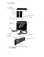
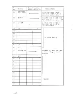
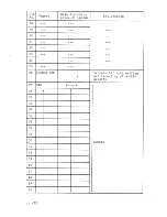
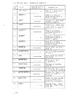
Page 80: ...2 M D D FDD card connec power unit ASSAC cird powe r cord buffer cabl e ryt ...

Page 81: ... I 2B y u T 8 1 J l I al lF I i llF I t __ _l 3 1 nqa lT r t t It lRrosI Jr F J I F a a ii d SS eil I l i ilLl Al R az rx trjEfi iffi rc34 L l i L ros li t t ti l If zo f f L j T i 10 i3 rer Tl v i I r o l h j H r i ii W a4 i I ezez ffi zu t 5u 6 l t Rzoo a t l 4 l l i f it tlJ a r L rH 3 f il i iEili9 l At I f ffi I i o I r ll c 4v _ ctoo ctot croz 5 P DzooB rror I i J uorj Q200 i i ctis n I i i ...

Page 82: ......

Page 83: ... p f f r 1 P x B e f f 1 n j r i r M E t N 4 r _ 4 u trHE E l t 7E9 E ...

Page 84: ...D7 LS74AP I z rltft RA6a tox R563 t5r tc64l HO7alS35 r 1 a 7 t 3 v ta Caat r i loltf s r tt ra f t l t t rG6a tor u f I ctalF cGxt 3i9l lCtl rot 1 2 tc6l7 HN4C27l 6 DD 1 J_ T ROM rc6r9 HD74LS74AP ItrailE l l l3r9 7X io o J n a t t c56t 2 tox ao ua J rc628 HO74LS93P 2 a t tl I c63i rODt I c x l c 6 I 2 HO74LS r OP tc6l I HD74LS I 4P lc6t lD7 rLSTaAP lil ilE lc6t 4 l0TaLsTaAP li ail E rc62l SNT LSTC...

Page 85: ...l 1 1 I rc648 i5v HoTaLsr23P c6r6 c67l t l t r t 1 J a a t orPEcTror ri ffEF fRtrE oATA fNITE 6ATE r AO LOIO r f r r i c r r l a r x L L a c 6 7 5 I l c a 7 a l c6t5TTTTc676 top so t c x c rc645 HOTaO6P C6rg L to r 9 J cx c L659 2 2y4 ttltaa t o ollto cx z 4c655 Q642 2SA76AY i r a t ff i riat ll II F o o F Gio o o f cNo C l 2 9 F r C 5 O F C t 5 9 F 1 o 1T I r c l o 5 fo t ca TI TTI ITTTT tl tttc ...

Page 86: ...OR m oFF cr 08 x7a3alr H r t t r lcl 9 lrt HD7 LSI 23P rcr07 HOT LSl aP tl lrfr t c l l 4 loT LsoP l c l t 6 5v lDTaLsT4AP lftlb g6iii cx l r 0r tflo Darr rcr09 I O 7 a L S r 2 3 P MOTOR ON OFF I lGl 05 r errrl Hoztoot g 7o l 2 A I t c t r 3 HD74LS TOP r 1 v r c r r E HOTaLSTrrAP tv nrc l c r l 5 HO74LS 32P t cl 05 xo7406P rrrrrf l f rrl 1_l TITTTT I i ITTTi ir w l ozcc rcrro e PJ1 ir ijr lraep _ ...

Page 87: ..._e AD El lABLE 1 exaBE 5 EPEED 6ffi R ra lx 4 l R fli cl J r l T nl R I 5l l 7n Rd tr I I I I I Pt R N EST A 1 4 00 Jtr e q 3 c DIS K CHf l CE 6D Rl J i tzr iD R O te Rl2 t o D r A q R q l D5 S E yc ul r JJ 1 Ir5t g r r J 3 q J J z r I r r i tfbi ffr9d JJ3 f rffi T C ffi aNtEx r l0TcH o E N ...

Page 88: ... osfi R35 l J9 r t cf 5 o ot97 R5 3 8r l Y q R 5 lF t 5 IB 6 i l H 4 c lr Qt 8 4 l ERASE r l J1 23 t50 1 5 t R86 Itll lVo T8 zsrrEd nFf 3O cJP Rqr R8 l t lE l i1 tl6 JZ I rs o trc R5 I I K c2l o Ui c o tf I K L I J10r ct 1p t tz Ra t t l i st e6l t O E T i __ f zx9 60 J J t i l R6 t0r I rrt I Pro6 56o 1i T f q t 3 t R t J trU4 to cr8 a 0l et l 63P t f o 6 a FF t o T Frq t E r A I lr 7 H I s 7 H t ...

Page 89: ...12 s3l3l1g T c3 l zl tocoT 5D SiAiorr sL P f 42 r9 r q tl D CrNt qNi 5V Y t FI H F t A I G FINE cLA P r rcR0 su tTCH 7S l I sr rt t p G r l t I lS 1 i l l i i Ui l as I it i 7T I l N x l v I F tr iv l tr I I iqls lnn o l iut ieFis l l a l lEsi j t l t F i 1rn 5 i i t l erer I cP lF i l l x I L v a I o t 9 4 l urfi Fl U lr 7 ...

Page 90: ...r0 K 1 I t I fjrege i r 3 4 5 i t f roD t 4 A t 7 I 9 7 HFA I AD serENtJ D i t 9 ACT ITlT I_Ef Rrl t o t aeRllcv SDLENDlE oPTrcN READ sErECr 1N trX o boz A 1 1 o0 Jtr t O e 3q e D I S K CH t6E 6D I I l i FADEI IABLE It E1 ltzl aF 2ql DI i fT tc I j rr It A Ve ENABE OR TE PRBT ...

Page 91: ...rtd TH Y R8q t lE l 86 R I c 5607 R5 l I K 5 ERAse a FF0ELAY zz I R61 z5x R f ro0 c filop t t2 t 3 l b l A Ft L r rt0 2JE gl 6 I rEo zW z i REAI tir 1 A c2t o t i ctl top Tt T8 zsrrSCrnFf 3o cJp Rqr L I or ct lP I K I t c o lf F l l 31 t lit 777 Rlt r l l i L2 s40 o c l 0 1 r hs f lt lK h tv r f trt4 toc CJg o otl A A F9g Arirl fr r p3 Dt loti it r t5 lSro G cr5 0ot7 1 i ctb 6 7rr s i3l tR cItl z ...

Page 92: ...l3t tR T t t T 7 ctt FU4 tot o rr p r f t 5 I B L H itrF cg FJ T Jjt D c g cr t a ot 6 Bp lSro fS A TR AC F Ci zsc t3rlR 5D SfrA iozr l l STEPPER M9T9R t s I I E Ll3i r 3 t Q p I r 3 i3 r rA Rll Its looK Tl ...

Reviews: