background image

DV-P2E

DVD  PLAYER

1. SAFETY INFORMATION ...................................... 2

2. EXPLODED VIEWS AND PARTS LIST ................ 3

3. SCHEMATIC DIAGRAM ..................................... 10

4. PCB CONNECTION DIAGRAM .......................... 24

5. PCB PARTS LIST ............................................... 33

6. ADJUSTMENT .................................................... 38

CONTENTS

7. GENERAL INFORMATION ................................ 46

    7.1  DISASSEMBLY ........................................... 46

    7.2 BLOCK DIAGRAM ........................................ 47

8. PANEL FACILITIES AND SPECIFICATIONS .... 48

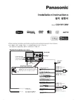
THIS MANUAL IS APPLICABLE TO THE FOLLOWING MODEL.

 Refer to the service guide for DV-P2E.

   IC information is described in the service guide.

STANDBY

FL OFF

0

7

1

4

¡ ¢

£¥8

'

DIGITAL VIDEO

96 kHz

ANGLE

TITLE

CHP/TRK

REMAIN TOTAL

GUI

DOLBY
DIGITAL

with

LAST MEMORY

POWER

OFF

_

STANDBY/ON

DVD  PLAYER

ÛN¿◊<x

l

e

d

o

M

t

n

e

m

e

r

i

u

q

e

R

r

e

w

o

P

l

a

n

o

i

g

e

R

e

d

o

c

n

o

i

t

c

i

r

t

s

e

r

E

2

P

-

V

D

V

0

4

2

0

2

2

C

A

2

Summary of Contents for DV-P2E

Page 1: ...NEL FACILITIES AND SPECIFICATIONS 48 THIS MANUAL IS APPLICABLE TO THE FOLLOWING MODEL Refer to the service guide for DV P2E IC information is described in the service guide STANDBY FL OFF 0 7 1 4 8 DIGITAL VIDEO 96 kHz ANGLE TITLE CHP TRK REMAIN TOTAL GUI DOLBY DIGITAL with LAST MEMORY POWER OFF_STANDBY ON DVD PLAYER ÛN x l e d o M t n e m e r i u q e R r e w o P l a n o i g e R e d o c n o i t c ...

Page 2: ...DVDM assy In the test mode the laser diode oscillates when microproces sor detects a PLAY signal or when the PLAY key is pressed S107 ON in the FLKB assy with the above requirements satis fied 2 When the cover is open close viewing through the objective lens with the naked eye will cause exposure to the laser beam Refer to page 40 Printed on the Rear Panel 1 SAFETY INFORMATION This service manual ...

Page 3: ...ector A PIVHB1060 12 Protector B PIVHB1061 13 Packing Case PIVHG1765 14 Mirror Mat Sheet PIZ23 007 15 Serial Number Label PIRRW 168 1 PACKING PARTS LIST Mark No Description Part No 2 EXPLODED VIEWS AND PARTS LIST NOTES Parts marked by NSP are generally unavailable because they are not in our Master Spare Parts List The mark found on some component parts indicates the importance of the safety facto...

Page 4: ...ON PARTS LIST Mark No Description Part No 12 Tray Stopper PIVNL1739 13 Tray Label PIVRW1628 14 Screw PIBPZ26P080FZK 15 Screw PIIBZ30P080FMC 16 Screw PIBCZ40P060FNI 17 Screw PIBBZ30P080FMC 18 Caution Label PIVRW1697 19 Power Button Joint PIVNK4179 20 Power Button PIVNK4374 Mark No Description Part No 16 18 1 14 9 8 10 17 16 19 20 15 2 3 4 Refer to 2 3 FRONT PANEL SECTION 15 5 13 11 12 Refer to 2 4 ...

Page 5: ... 8 Main Key PIVNK4373 9 10 PLAY Lens PIRNK2232 1 FRONT PANEL SECTION PARTS LIST Mark No Description Part No 11 FL Filter PIVEC1643 12 Illumination Lens PIVNK4168 13 Illumination Filter PIVEC2012 14 Illumination Holder PIVNK4098 15 Flexible Cable 14P PIVDA1646 FLKB CN101 DVDM CN105 16 Screw PIBBZ30P080FMC Mark No Description Part No 6 4 7 8 1 3 8 2 3 8 3 3 15 3 1 16 10 14 11 13 12 5 16 2 ...

Page 6: ...6 25 Refer to 2 5 LOADING MECHANISM ASSY 4 7 11 23 23 1 12 23 31 28 12 17 23 15 16 18 3 19 21 23 20 23 29 30 23 23 24 23 23 23 10 13 14 10 2 22 23 23 6 8 5 8 23 2 4 BOTTOM VIEW SECTION ...

Page 7: ...84 15 Guard PIVNK4100 1 BOTTOM VIEW SECTION PARTS LIST Mark No Description Part No NSP 16 Chassis PIVNA1876 17 Insulator PIPNW2766 18 Insulator Assy PIVXA1680 19 Flexible Cable 14P PIVDA1646 AVJB CN191 DVDM CN803 20 Flexible Cable 17P PIVDA1650 AVJB CN901 DVDM CN802 21 Rear Panel PIVNA2015 22 Housing Assy 4P PIVKP2157 DVDM CN801 AVJB CN301 23 Screw PIBBZ30P080FMC 24 Screw PIBBZ30P180FMC 25 Screw P...

Page 8: ...34 LOADING MECHANISM ASSY PARTS LIST Mark No Description Part No 11 Loading Motor Assy PIVXX2505 12 DC Motor PIPXM1027 13 Motor Pulley PIPNW1634 NSP 14 LOMB Assy PIVWG1886 15 Connector Assy 2P PIPG02KK E35 LOMB CN401 LOSB CN303 16 Screw PIVBA1055 17 Screw PIZ39 019 18 Flexible Cable 8P PIVDA1649 LOSB CN302 INSB CN202 19 20 Stopper PIDNH2076 Mark No Description Part No 11 13 12 14 15 16 8 7 17 9 10...

Page 9: ...Mechanism Base PIVNL1748 13 Hook PIVNL1770 14 Hook Spring PIVBH1291 15 Slider PIVNL1745 16 HOLD SPRING PIVNC1011 NSP 17 Pickup Assy PIVWY1046 SERVO MECHANISM ASSY PARTS LIST Mark No Description Part No 18 Floating Rubber PIDEB1315 19 Float Base PIVNL1732 20 Gear D PIVNL1766 21 Gear Spring PIVBH1279 22 Gear E PIVNL1767 23 Gear F PIVNL1768 24 Motor PIVXM1062 NSP 25 INSB Assy PIVWG1883 26 Screw PIPBZ...

Page 10: ... H DVDM ASSY PIVWS1371 I L G DILB ASSY PIVWG1881 F E 1 3 3 3 FLKB ASSY PIVWG1876 PWSB ASSY PIVWG1937 AVJB ASSY PIVWV1575 SCCB ASSY PIVWV1577 SR IN 3 1 OVERALL CONNECTION DIAGRAM LOMB LOSB INSB AND FGSB ASSEMBLIES 3 SCHEMATIC DIAGRAM ...

Page 11: ... PIVWG1884 LOADING MOTOR ASSY VXX2505 CN401 B2B PH K S CN303 B2B PH K S LOAB ASSY PIVWM1798 SMEB ASSY PIVWM1797 CN302 VKN1268 CN301 VKN1272 CN202 VKN1239 CN101 B3B PH K S CN201 B3B PH K S PC101 GP2S27 B S201 S301 SPINDLE MOTOR ASSY VXX2563 VXM1062 PICKUP ASSY PIVWY1046 RF SIGNAL ROUTE FOCUS SERVO LOOP LINE SLIDER SERVO LOOP LINE TRACKING SERVO LOOP LINE F T S F F F F F F T T T F F T T T S S S S S ...

Page 12: ...12 A B C D 1 2 3 4 1 2 3 4 E FLKB ASSY PIVWG1876 FL TUBE R197 0 R198 0 0 C111 0 1 C114 0 1 C113 0 1 3 2 FLKB PWSB AND DILB ASSEMBLIES E ...

Page 13: ...SY PIVWG1937 G DILB ASSY PIVWG1881 AC1 AC2 H 2 3 CN105 SLP9118C51H D201 D202 SLP4118C51H REMOTE RECEIVER UNIT R201 180 R118 R120 62 PWSB ASSY S202 FL OFF FLKB ASSY S102 S103 S104 S105 S106 OPEN CLOSE REV FWD STOP PLAY PAUSE C112 0 1 G F E ...

Page 14: ...10393F 2 2 1 2 R177 33k R178 33k VKN1416 CN107 B CN301 J CN201 PICKUP ASSY CN102 VKN1445 S14B PH SM3 CN101 VKF1001 TP400 VKF1001 TP100 VKF1001 TP300 CN201 VKN1324 2 2 1 2 VTL1074 L342 VTL1074 L335 VTL1074 L340 6 6 5 6 1 6 4 6 3 6 2 6 H 2 3 H 2 3 H 2 3 H 3 3 DVDM ASSY 1 3 PIVWS1371 H1 3 VCO Offset ADJ 3 3 DVDM ASSY 1 3 1 3 H ...

Page 15: ...F F F F T T T T T S S AGCOFF LD ON IC506 TC74VHCT245AFT VKF1001 TP200 IC501 PD4889A IC504 TC74VHC20FT IC505 1 2 TC74VHC139FT IC505 2 2 TC74VHC139FT SRM2B256SLMX70 IC201 LC78650NE C271 4700p R271 150k R273 220k R277 100k R275 33k R276 150k 2 2 1 2 H 2 3 H 2 3 H 2 3 H 2 3 H 3 3 XRESET DOUT SBSY PW SFSY SBCK LRSY ROMCK ROMXA MON C2F FG LEVEL SHIFT 1 3 H ...

Page 16: ...Hz IC605 2 2 TC74VHC139FT IC605 1 2 TC74VHC139FT ADDRESS DATA A2 A10 C2F XRESET H 3 3 H 3 3 H 1 3 XCSDOLV DOLV CD XWRL XWRH XRD XLT3 XAMUTE XDREQ1 HCPUCK IR SEL IR XDVRST1 XAVIRQ0 48 X44 HIBSEL XCS6 XDACK1 NAP SW H 3 3 H 1 3 H 2 3 DVDM ASSY 2 3 PIVWS1371 3 4 DVDM ASSY 2 3 2 3 H ...

Page 17: ...L ROUTE ROM DATA SIGNAL ROUTE ROM ROM ROM ROM ROM ROM ROM ROM VKN1418 CN105 SERVO MONITOR OUTPUT E CN101 H H H H 3 3 3 3 3 3 1 3 H 1 3 H 3 3 H 3 3 H 3 3 H 1 3 H 1 3 H 3 3 H 3 3 H 1 3 H 3 3 H 1 3 H 3 3 SDATA H 1 3 IC817 TC74VHCT541AFT 2 3 H ...

Page 18: ... 1 4 3 4 4 4 4 4 3 4 3 3 1 3 2 3 1 4 2 4 2 4 S4B PH SM3 CN801 IC813 CY2081SL 611 4 4 3 4 2 4 DVDM ASSY 3 3 PIVWS1371 1 4 H 3 3 I CN301 H 2 3 H 2 3 H 2 3 H 2 3 H 2 3 H 1 3 H 1 3 H 2 3 H 2 3 H 2 3 H 2 3 H 2 3 H 2 3 Video Output Level ADJ 3 5 DVDM ASSY 3 3 3 3 H ...

Page 19: ...OMPOSITE VIDEO SIGNAL ROUTE Y SIGNAL ROUTE C SIGNAL ROUTE ROM DATA SIGNAL ROUTE COM Y C ROM COM COM COM COM Y Y Y Y C C C C C IC901 2 2 1 2 2 2 1 2 VKN1418 CN803 VKN1421 CN802 I CN191 I CN901 HIBSEL 48 X44 XRESET XLT3 XAMUTE H 2 3 H 2 3 H 2 3 3 3 H ...

Page 20: ...20 A B C D 1 2 3 4 1 2 3 4 H 3 3 H 3 3 CN802 CN803 H 3 3 CN801 TC7WU04F TC7WU04F C Y COM C Y COM C Y COM C COM IC101 PD2029A L SR IN 18MHz Master Clock ADJ R5020 0 R3080 0 3 6 AVJB ASSY I ...

Page 21: ...6 7 8 AVJB ASSY PIVWV1575 I COMPOSITE VIDEO SIGNAL ROUTE Y SIGNAL ROUTE C SIGNAL ROUTE AUDIO SIGNAL ROUTE COM Y C COM Y C C C C C Y Y Y COM COM COM L CN100 D501 MA111 D601 MA111 R20 0 R16 0 R60 0 R17 R19 R21 0 0 0 82P 82P I ...

Page 22: ...514 1SS270A R411 JMP R312 10K R514 10K 100 35V C512 R512 22K C511 47 50V C411 330 35V IC711 IC411 VZF1048 VZF1060 C412 56 35V C711 47 35V 1K R513 1K C612 0 01 50V C611 0 01 50V R611 3 9 IC201 AN1431T R206 1 5K R204 1 6K R205 200 D512 1SS270A C107 C120 C108 S3L20U VZF1059 13 14 15 16 12 10 11 C201 0 47 50V 10UH D106 2 2 C314 33 35V D110 VZF1045 D103 RD18FB2 RKP1751 CN10 C10 0 01 250 ACG7010 K MSWB ...

Page 23: ...23 A B C D 1 2 3 4 1 2 3 4 L SCCB ASSY PIVWV1577 I CN19 3 8 SCCB ASSY L ...

Page 24: ...low 3 The parts mounted on this PCB include all necessary parts for several destinations For further information for respective destinations be sure to check with the schematic diagram 4 View point of PCB diagrams Symbol In PCB Diagrams Symbol In Schematic Diagrams Part Name B C E D D G G S S B C E B C E D G S B C E B C E B C E Transistor Transistor with resistor Field effect transistor Resistor a...

Page 25: ...25 A B C D 1 2 3 4 1 2 3 4 PWSB ASSY F DILB ASSY G PWSB ASSY F DILB ASSY G CN102 E CN103 E PIVNP1625 B PIVNP1625 B PIVNP1625 B PIVNP1625 B 4 2 PWSB AND DILB ASSEMBLIES F G SIDE A SIDE B ...

Page 26: ...26 A B C D 1 2 3 4 1 2 3 4 FLKB ASSY E FLKB ASSY E Q105 CN201 F 4 3 FLKB ASSY E SIDE A SIDE B ...

Page 27: ...27 A B C D 5 6 7 8 5 6 7 8 PIVNP1625 B Q103 IC102 PIVNP1625 B CN301 G CN105 H Q105 IC101 Q101 Q107 Q106 Q104 Q108 E ...

Page 28: ...6 IC401 IC302 IC303 Q301 IC701 IC203 IC202 IC806 IC204 IC161 IC271 IC824 IC902 IC813 IC818 IC820 IC814 IC810 IC811 IC815 IC816 Q802 Q105 Q102 Q873 Q455 Q801 Q891 IC206 IC171 IC151 Q291 IC807 IC801 IC501 Q401 Q403 PIVNP1624 C 4 4 DVDM ASSY H SIDE A This PCB is a four layered board Middle layer is mainly connected to Vcc and GND ...

Page 29: ...H PIVNP1624 C IC505 IC605 IC504 IC502 IC503 IC301 IC703 IC817 IC702 IC201 IC205 IC808 IC809 IC805 IC821 IC802 IC901 IC804 IC101 Q261 Q106 Q107 Q103 Q104 Q108 Q110 Q851 Q871 Q831 Q852 Q872 Q832 IC604 IC603 IC602 Q771 Q772 Q601 Q603 SIDE B H ...

Page 30: ...30 A B C D 1 2 3 4 1 2 3 4 AVJB ASSY I CN801 H CN803 H CN802 H CN100 L PIVNP1626 B VC301 IC102 IC201 IC101 IC191 Q502 Q501 Q602 Q601 IC701 IC901 4 5 AVJB ASSY I SIDE A ...

Page 31: ...31 A B C D 1 2 3 4 1 2 3 4 AVJB ASSY I PIVNP1626 B IC301 IC306 Q121 Q124 Q221 Q224 Q511 Q514 Q521 Q524 IC701 IC901 IC102 IC201 I SIDE B ...

Page 32: ... 2 3 4 1 2 3 4 CN100 POWER SUPPLY ASSY J MSWB ASSY K SCCB ASSY L PIVNP1626 B PIVNP1629 A CN101 H AC IN CN19 I Q101 Q103 IC201 Q511 IC411 IC711 Q108 Q107 SIDE A 4 6 POWER SUPPLY MSWB AND SCCB ASSEMBLIES J K L SIDE B ...

Page 33: ...ere are 3 effective digits such as in high precision metal film resistors 5 62k Ω 562 101 5621 RN1 4PC 5 6 2 1 F 5 1 LIST OF WHOLE PCB ASSEMBLIES k r a M n o i t p i r c s e D d n a l o b m y S o N t r a P s k r a m e R E 2 P V D P S N P S N P S N P S N P S N P S N P S N P S N P S N P S N Y S S A B A O L Y S S A B M O L Y S S A B S O L Y S S A B E M S Y S S A B S N I Y S S A B S G F Y S S A Y K L ...

Page 34: ...DER PIDEF1012 CN202 8P FFC CONNECTOR PIVKN1239 FGSB ASSY SEMICONDUCTOR PC101 PIGP2S27 B RESISTORS All Resistors PIRS1 10S J OTHERS CN101 KR CONNECTOR 3P PIB3B PH K S FLKB ASSY SEMICONDUCTORS IC101 PIPD4890A IC102 PIS 806D Q103 PIDTD113ES D112 PIEP05Q04 SWITCHES S102 S106 PIRSG1030 CAPACITORS C101 C102 PICEJA470M6R3 C117 C125 C128 PICKSQYB102K50 C111 C114 PICKSQYF104Z25 RESISTORS All Resistors PIRS...

Page 35: ...A Q871 Q872 PIIMT1A Q103 Q402 Q873 PIIMX1 Q102 Q104 Q291 Q301 PIIMZ1A Q106 Q603 PIPDTA114EK Q107 Q109 Q261 Q602 PIPDTC114EK Q601 Q771 Q772 PIPDTC114TK D301 PIKV1410 D171 D172 PIMA152WK D601 PIRB501V 40 COILS AND FILTERS F771 F778 F779 CHIP BEAD PIDTF1067 L941 L942 L945 L946 PIQTL1011 CHIP SOLID INDUCTOR F896 FERRITE BEAD PIVTF1077 F801 VIDEO FILTER PIVTF1098 F401 F406 CHIP EMI FILTER PIVTH1037 L30...

Page 36: ...RA4C103J R703 R704 R717 R718 PIRA4C103J R745 R746 R761 R762 R792 PIRA4C103J R812 R813 PIRA4C103J R137 R501 R502 R505 R506 PIRA4C220J R604 R607 R712 R713 R719 PIRA4C220J R724 R748 R749 R791 PIRA4C220J R802 R803 R808 PIRA4C220J R602 R603 R610 R613 R618 PIRA4C470J R101 R11 R14 R141 PIRS1 10S0R0J R15 R17 R171 R18 PIRS1 10S0R0J R201 R203 R266 R300 R319 PIRS1 10S0R0J R333 R411 R413 R701 PIRS1 10S0R0J R7...

Page 37: ... OPTICAL MODULE PIGP1F32T JA401 REMOTE CONTROL PIRKN1004 JACK PCB BINDER PIVEF1040 JA601 1P PIN JACK PIVKB1063 JA901 1P PIN JACK NI BLK PIVKB1077 CN19 8P FFC CONNECTOR PIVKN1239 CN191 14P FFC CONNECTOR PIVKN1245 CN901 17P FFC CONNECTOR PIVKN1248 SCREW TERMINAL PIVNE1948 KN301 EARTH METAL PIVNF1084 X302 CRYSTAL 16MHz PIVSS1081 X301 CRYSTAL 18 432MHz PIVSS1116 POWER SUPPLY ASSY SEMICONDUCTORS IC201 ...

Page 38: ...djustment Note 1 Remove the tray when adjusting the tangential and radial adjustment screws Note 2 After the adjustment stabilize the screw with an adhesive Adjustment Points Mechanism Part 1 2 1 2 Radial adjustment screw 3 Tangential adjustment screw 1 2 1 2 CN201 CN101 CN201 1 2 FE 3 4 GNDS 5 6 RFO 7 8 GNDS 9 10 TE 11 12 VREF 13 TDO 14 FDO 1 1 1 13 2 14 VR801 VC301 1 2 DVDM ASSY 3 IC701 IC801 IC...

Page 39: ...lloscope with delay Frequency band 40MHz Frequency counter Display digit 8 digit TV monitor Test mode remote control unit PIGGF1067 6 2 JIGS AND MEASURING INSTRUMENTS Screwdriver small Precise screwdriver Screwdriver medium CH1 CH2 X Y Hexagonal screwdriver Jitter Meter LEVEL JITTER X1 27M Equalizer Unit ...

Page 40: ...CHECK DVD S CDV ESC TEST POWER ON TRAY OPEN REPEAT A DVD disc TRAY CLOSE REPEAT A e TEST MODE PLAY TEST MODE OFF PLAY TILT OFF TRKG OFF TILT OFF TRKG OFF PLAY TILT OFF N TRKG ON TILT OFF N TRKG ON OR PIGGF1067 Test mode remote control unit ESC OFF POWER TILT OFF TRKG ON TRACKING ON PLAY TRACKING OFF PLAY E TEST 2 TEST 5 ...

Page 41: ...GE PCB ASSY Note is adjusted already Ask the Region Setting end Mechanical point Electric point Exchange board DVDM ASSY Note and are adjusted already When replacing the FLASH MEMORY IC603 on the DVDM Assy follow the 6 5 REGION SETTING POWER ON 2 OR OR 1 2 3 Player s Region Setting 2 Region 2 4 Region 4 2 4 3 4 etc 3 4 2 etc Pick out any one of these Blinking Key input the number with the test mod...

Page 42: ...nts Mechanism assy CH1 CH2 X Y Max See Adjustment points Mechanism assy START RF 11T Max RF 11T LEVEL JITTER X1 27M Jitter Meter Probe 10 1 EQ UNIT Test mode TRKG Play the DVD test disc at outer track around 1F0000 Player ON 5 RFO CN201 DVDM ASSY Tangential Adjustment Screw Radial Adjustment Screw See Adjustment points Mechanism assy See Adjustment points Mechanism assy START TV monitor VIDEO OUT ...

Page 43: ...r ON Frequency counter Player START VC301 AVJB ASSY 27MHz 20Hz DVDM ASSY IC813 CH1 CH2 X Y Oscilloscope V 50mV div H 10msec div DC mode TV trigger VCO Offset Adjustment Normal mode Play the DVD test disc Probe 10 1 VC301 DVDM ASSY Player DVDM ASSY START 1 9V 0 1V 2 GND IC302 1 6 ...

Page 44: ...Video Output Level Adjustment Normal mode Still the DVD test disc 100 White Screen VIDEO OUT VIDEO IN Oscilloscope V 20mV div H 10µsec div AC mode TV trigger Probe 10 1 CH1 CH2 X Y TV monitor START VR801 DVDM ASSY 1Vp p ...

Page 45: ...OM and system controller Part No of DVD mechanism controller Address Tilt error value Tilt servo status Tracking status Spindle status AGC setting FTS servo IC information C1 error value of CD and DVD Internal operation mode of the mechanism control Disc judgment Pickup LASER DISC DIG ANA DISP TEST MODE ESC CX REP A REP B STEREO P N A MON TV LDP A B SCAN 3 CHAPTER SKIP PLAY 1 2 3 CLEAR 4 5 6 10 7 ...

Page 46: ... DISASSEMBLY DISC TRAY DVDM ASSY BONNET Note For the mechanism section disassembly refer to the service guide POWER OPEN CLOSE 1 2 4 1 1 1 1 1 1 1 2 2 2 3 3 1 1 4 3 2 5 3 4 DVDM ASSY Be careful of the flexible cable DVDM ASSY 6 6 ...

Page 47: ... ROM RAM SREO XSACK CPU I F Y C Comp PCM D Out AC3 D Out Lt Rt Video Out DVD V CD AV Decoder Display CPU SYSTEM Decoder DMUX AV Sync controller MPEG2 Video Decoder Sub picture Decoder GUI Memory Controller 16M bit SDRAM CODE Buffer Video Audio Sub picture GUI MIX D A AC3 MPEG1 Audio Decoder Copy Guard NTSC PAL encode DAC DAC DAC S PDIF LSI 11 IC802 MB811171622A 100FN IC604 TC551001BFL 85 IC603 VYW...

Page 48: ...chart on the right Coaxial Connect to the coaxial jack and select PCM from the menu Optical Connect to the optical jack and select PCM from the menu Coaxial Connect to the PCM jack and select PCM DOLBYDIGITALfrom the menu Optical Connect to the optical jack and select PCM DOLBY DIGITAL from the menu STANDBY indicator Display OFF button FL OFF Display window Reverse 41 button Forward button Disc il...

Page 49: ...layed Indicates total playback time of side Indicates the playback mode title type of disc etc as follows Indicates that title is being displayed Indicates Dolby digital playback Indicates GUI operation is being performed Indicated Multi Angle playback is in progress Indication location for Last Memory is being recorded in memory Indicates that playback settings condition have been memorized When ...

Page 50: ...LAY 3 Forward button FWD Display button DISPLAY Subtitle button SUBTITLE Open Close button OPEN CLOSE 0 Angle button ANGLE Menu operation buttons Direction buttons 2 3 5 Enter button ENTER Previous button PREV 4 Next button NEXT REMOTE CONTROL POWER OPEN CLOSE AUDIO SUBTITLE ANGLE DISPLAY 0 TITLE PREV NEXT MENU ENTER 4 5 2 3 RETURN REV PAUSE PLAY FWD STOP STEP 1 8 3 7 e E CLEAR PROGRAM CHP TIME 1 ...

Page 51: ...A U S E P L A Y F W D S T O P S T E P 1 8 3 7 e E C L E A R PROGRAM C H P T IM E 1 2 3 C 4 5 6 1 0 7 8 9 0 M O D E R A N D O M R E P E A T R E P E A T A B LA S T M E M O C O N D IT IO N Accessories Audio cord PIVDE1033 L 1 5m Video cord PIVDE1048 L 1 5m Power cord PIADG1154 Batteries 2 Warranty card Operating Instructions this manual Remote control unit PIVXX2595 White Red Yellow Other included it...

Page 52: ...1 CIRCUIT DESCRIPTION 2 2 TEST MODE 6 3 IC INFORMATION 15 4 FL INFORMATION 35 CONTENTS DV P2E DVD PLAYER SERVICE GUIDE ...

Page 53: ...Key SW Display System CPU 32 bit RISC FLASH ROM RAM SREO XSACK CPU I F Y C Comp PCM D Out AC3 D Out Lt Rt Video Out DVD V CD AV Decoder Display CPU SYSTEM Decoder DMUX AV Sync controller MPEG2 Video Decoder Sub picture Decoder GUI Memory Controller 16M bit SDRAM CODE Buffer Video Audio Sub picture GUI MIX D A AC3 MPEG1 Audio Decoder Copy Guard NTSC PAL encode DAC DAC DAC S PDIF LSI 11 IC802 MB8111...

Page 54: ... CONTROL IC151 DRIVER FOCUS SERVO FOCUS LOCK TIMING PH RF B1 B2 B3 B4 LD MD FOCUS COIL FE OEIC GAIN LASER ADDRESS BUS SGC FDO DRF 58 31 13 UP 1 2 2 Focus Servo FE generated in the RF IC is sent to the Digital servo IC For a DVD the servo is turned on during the transition from Up to Down of the first order sine wave For a CD it turns on during the transition from Down to Up of the first order sine...

Page 55: ...ICKUP IC101 RFIC IC201 DIGITAL SERVO IC IC501 MECH CONTROL IC151 DRIVER TRACKING SLIDER SERVO TE TE RF B1 B2 B3 B4 TRKG COIL TBAL ADDRESS BUS TDO 19 SLDO M 26 28 CP SLDR 3 12 41 57 48 25 95 OEIC IC101 RFIC IC301 A D IC701 LSI II IC201 DIGITAL SERVO IC161 DRV SPDL SERVO RFO RF CLK 27M 8 bit ATC APC AFC ASC V165 DUTY50 FG VPWM PPWM RPWM FPWM 31 50 32 RF IC302 1 2 IC271 2 2 IC271 1 2 FG SPDL SPDL SPD...

Page 56: ...wave detected at the first lens sweep is of a value less than 0 5 V the OE IC gain is set to H and the peak to peak value of the sine wave is roughly adjusted to 1 8 Vp p By sweeping the lens around the height where the sine wave has been detected disc determination is performed and the sine wave is finely adjusted to 1 8 Vp p Offset compensation Lens sweep Lens sweep NO DISC OEIC gain H FCS AMP g...

Page 57: ... pressed in the address input mode input mode changes to hexadecimal number input Indicates mark and 1 to 6 keys are input as A to F At this time 7 8 9 and 0 keys are not accepted Also the hexadecimal number input and the decimal number input can be changed with toggle 8 Search Practice 1 Press CHP TIM 13 key of the remote control unit Practice the on screen no playback Doesn t demultiplex after t...

Page 58: ... manual moves in the going down direction when SKIP REV 53 key of the remote control unit is pressed during the play at the time of tilt off 19 Tilt Up A manual moves in the going up direction when SKIP FWD 52 key of the remote control unit is pressed during the play at the time of tilt off 20 Focus Jump Focus jumps in 1 layer from 0 layer when MULTI FWD 58 key of the remote control unit is presse...

Page 59: ...the address four digits of the coefficient that it wants to see by the point of search address input then real time indicates the coefficient in OSD by pressing TEST and 9 keys in order 8 CD Error Rate Indication Indicate the value in OSD after measuring is completed by pressing TEST and 0 keys in order after set up the measuring time 1 to 8 seconds by the point of search address input 2 5 EXPANSI...

Page 60: ...vo off Tilt On N SKIP REV A8 53 SKIP FWD A8 52 Tilt up PLAY SKIP FWD A8 52 Tilt down PLAY SKIP REV A8 53 LD on TEST 1 A8 5E A8 01 Focus on TEST 2 A8 5E A8 02 Focus sweep TEST 3 A8 5E A8 03 Focus jump MULTI FWD A8 58 Focus jump MULTI REV A8 55 Spindle FG on TEST 5 A8 5E A8 05 AGC on off AGC Off On TEST 7 A8 5E A8 07 Indication of the FTS coefficient After the address four digit input TEST 9 A8 5E A...

Page 61: ...V 1 chip version Part No of flash ROM and system controller Part No of DVD mechanism controller Address Tilt error value Tilt servo status Tracking status Spindle status AGC setting FTS servo IC information C1 error value of CD and DVD Internal operation mode of the mechanism control Disc judgment Pickup Caution The first screen and second screen switch by pressing DISPLAY key of the remote contro...

Page 62: ... AGC AGC on ON AGC off OFF 10 Output video system V NTSC system NTSC PAL system PAL Auto setting AUTO 11 FTS servo IC information Indications for the following two types of information can be switched DSP coefficient indication KS Displays the address four digits of the specified coefficient and the setting value four digits with TEST and 9 keys Jitter value indication JT Displays the jitter value...

Page 63: ...yback state 2 Set the player to Number input mode by pressing 10 and enter the measurement time in a range of 1 to 5 sec 3 Start measurement by pressing TEST 0 The SubQ counter stops during measurement but this is not a malfunction When the specified measurement time has elapsed the result is indicated to the right of ER C1 on the screen If you skip step 2 the measurement time is set to 5 sec 2 8 ...

Page 64: ...isc distinction are discussed in the next section Using the Function in Test Mode This function is not assigned to any remote control keys Only an open close operation can trigger the function 2 8 6 SGC Overview This is a new function to maintain the sine wave related to focus errors to a certain size so that the sine wave shows 1 8 V for the P to P value This operation is performed each time afte...

Page 65: ...justments 4 Spindle Errors Errors 48 49 An FG transition timeout Error 48 may be generated because of instability of the FG signal or unavailability of spindle drive voltage A PLL transition timeout Error 49 can be generated with a dirty disc 5 Automatic Sequence Errors Errors 51 to 55 If any automatic sequence auto execution command of the servo DSP is not completed these errors are generated The...

Page 66: ...TP3 P03 INTERRUPT CONTROL INTP3 CI0 P03 INTP0 TI0 P00 CLOCK OUTPUT CONTROL BUZ P36 PCL P35 A D CONVERTER SO1 P21 SCK1 P22 STB P23 BUSY P24 SI1 P20 SERIAL INTERFACE 0 SERIAL INTERFACE 1 SO0 SB1 P26 SI0 SB0 P25 SCK0 P27 SYSTEM CONTROL WATCHDOG TIMER WATCH TIMER BUZZER OUTPUT P01 P03 P00 P04 P10 P17 P20 P27 P30 P37 P70 P74 P80 P81 P90 P97 P100 P107 P110 P117 P120 P127 FIP0 FIP33 VLOAD RESET X1 X2 XT1...

Page 67: ... I S I r e l l o r t n o c m e t s y s e h t h t i w t u p n i a t a d n o i t a c i n u m m o C 7 1 T E S E R N I T E S E R I t e s e r L t u p n i t e s e R 8 1 4 7 P C N O d e s u t o N 9 1 3 7 P C N O d e s u t o N 0 2 s s V A s s V n i p D N G 1 2 7 1 P N O R E W O P O N O H F F O N O V 5 W S 2 2 6 1 P T U O T E S E R O t e s e r L t u p t u o t e s e r m e t s y S 3 2 5 1 P C N O d e s u t o...

Page 68: ... 0 5 1 7 P D E L F F O L F O N O L F F O N O D E L F F O L F 1 5 0 7 P C N O d e s u t o N 2 5 V D D V D D n i p y l p p u s r e w o P 3 5 7 2 1 P C N O d e s u t o N 4 5 6 2 1 P C N O d e s u t o N 5 5 5 2 1 P C N 6 5 4 2 1 P C N 7 5 3 2 1 P C N 8 5 2 2 1 P C N 9 5 1 2 1 P C N 0 6 0 2 1 P C N 1 6 7 1 1 P 5 1 P O N O H t u p t u o t n e m g e s L F 2 6 6 1 1 P 4 1 P 3 6 5 1 1 P 3 1 P 4 6 4 1 1 P 2...

Page 69: ...2 GND MIXO2 1 2 3 4 5 6 7 8 9 10 11 12 13 14 15 16 17 18 19 20 21 22 23 24 25 26 27 28 29 30 31 32 50k 50k 80k 80k 80k 80k 45k 64 63 62 61 60 59 58 57 56 55 54 53 52 51 50 49 48 47 46 45 44 43 42 41 40 39 38 37 36 35 34 33 BH PH BH PH Scratch Detection 40k 40k 60k 60k 26p 26p 40k 40k PD PD PD PD LIM LIM LIM LIM LIM 60k 80k 80k 60k REF VCC 26p REF REF REF VCC VCC REF REF REF REF REF APC CP 50k 3k 3...

Page 70: ...n o C n o N 5 1 C N 3 C N 6 1 C N 4 S A I B n i p s a i B 7 1 V C C n i p y l p p u s r e w o P 5 N I R D n i p t n e m t s u j d a n i a g r e v i r D 8 1 C N n o i t c e n n o C n o N 6 N I R D n i p t u p n i n i a g r e v i r D 9 1 D N G n i p D N G t i a r t s b u S 7 C N n o i t c e n n o C n o N 0 2 D N G 8 C N 1 2 C N n o i t c e n n o C n o N 9 C N 2 2 E T U M n i p e t u M 0 1 C N 3 2 C ...

Page 71: ...X 1 1 1 D A M 3 4 p p V C I D N G 2 1 2 D A M 4 4 2 T X d e s u t o N 3 1 3 D A M 5 4 K P P D V D I d e s u t o N 4 1 4 D A M 6 4 s s V A D N G 5 1 5 D A M 7 4 S O P D O L I t u p n i W S n o i t i s o p p m a l c d n a g n i d a o L 6 1 6 D A M 8 4 S O P D L S I t u p n i W S n o i t i s o p r e d i l S 7 1 7 D A M 9 4 S O P R O D I d e s u t o N 8 1 8 A M O s u b s s e r d d a l a n r e t x E 0 ...

Page 72: ...D CS OE WE 12 14 18 13 15 16 17 18 19 o N e m a N n i P n o i t c n u F o N e m a N n i P n o i t c n u F 1 4 1 A t u p n i s s e r d d A 5 1 4 O I t u p t u o t u p n i a t a D 2 2 1 A 6 1 5 O I 3 7 A 7 1 6 O I 4 6 A 8 1 7 O I 5 5 A 9 1 8 O I 6 4 A 0 2 S C t c e l e s p i h C 7 3 A 1 2 0 1 A t u p n i s s e r d d A 8 2 A 2 2 E O e l b a n e t u p t u O 9 1 A 3 2 1 1 A t u p n i s s e r d d A 0 1 ...

Page 73: ...P r o 0 1 5 2 8 1 A t u p n i s s e r d d A 4 2 4 Q D t u p t u o t u p n i a t a D 3 7 1 A 5 2 2 1 Q D 4 7 A 6 2 5 Q D 5 6 A 7 2 3 1 Q D 6 5 A 8 2 6 Q D 7 4 A 9 2 4 1 Q D 8 3 A 0 3 7 Q D 9 2 A 1 3 1 A 5 1 Q D t u p n i s s e r d d a t u p t u o t u p n i a t a D 0 1 1 A 2 3 V S S d n u o r G 1 1 0 A 3 3 E T Y B s e d o m t i b 6 1 d n a t i b 8 e h t h c t i w S 2 1 E C e l b a n e p i h C 4 3 6 ...

Page 74: ...9 AD13 18 AD12 17 AD11 16 AD10 14 AD9 13 AD8 11 AD7 10 AD6 9 AD5 8 AD4 7 AD3 6 AD2 5 AD1 4 AD0 PB0 TP0 TIOCA2 PB1 TP1 TIOCB2 100 PB2 TP2 TIOCA3 101 PB3 TP3 TIOCB3 102 PB4 TP4 TIOCA4 103 PB5 TP5 TIOCB4 104 PB6 TP6 TOCXA4 TCLKC 105 PB7 TP7 TOCXB4 TCLKC 107 PB8 TP8 RxD0 108 PB9 TP9 TxD0 109 PB10 TP10 RxD1 110 PB11 TP11 TxD1 111 PB12 TP12 IREQ4 SCK0 112 PB13 TP13 IREQ5 SCK1 PB14 TP14 IREQ6 PB15 TP15 I...

Page 75: ... l i b t i b 6 1 4 1 9 D A 5 1 C C V I y l p p u s r e w o P 6 1 0 1 D A O I s u b a t a d l a r e t a l i b t i b 6 1 7 1 1 1 D A 8 1 2 1 D A 9 1 3 1 D A 0 2 4 1 D A 1 2 5 1 D A 2 2 S S V I d n u o r G 3 2 S B H 0 A O l a n g i s e b o r t s e t y b r e p p u t u p t u o s u b s s e r d d A 4 2 1 A O t u p t u o s u b s s e r d d A 5 2 2 A 6 2 3 A 7 2 4 A 8 2 5 A 9 2 6 A 0 3 7 A 1 3 S S V I d n u...

Page 76: ... T U O Q R I H A 9 A P O I e v a l s t a t u p t u o t s e u q e r n o i t p u r r e t n I l a n g i s g n i m i t d l o h s s e r d d A A t r o p t u p t u o t u p n i t i b 6 1 t u p n i r e g g i r t n o i s r e v n o c D A 4 6 1 A C O I T L P D 0 1 A P O I e d i s r e w o l e h t n o y t i r a p s u b a t a D A t r o p t u p t u o t u p n i t i b 6 1 1 l e n n a h c t u p t u o e r a p m o c t...

Page 77: ... 4 B C O I T 5 P T 5 B P 4 0 1 C K L C T 4 A X C O T 6 P T 6 B P O I 4 l e n n a h c t u p t u o e r a p m o c t u p t u o U T I t u p t u o n r e t t a p g n i m i T B t r o p t u p t u o t u p n i t i b 6 1 t u p n i k c o l c r e m i t U T I 5 0 1 D K L C T 4 B X C O T 7 P T 7 B P 6 0 1 S S V I d n u o r G 7 0 1 0 D X R 8 P T 8 B P O I 0 l e n n a h c t u p n i a t a d e v i e c e R t u p t u o...

Page 78: ...ecoder Block System Clock Clock for video Clock for audio LPF VCO Clock Signal Video Output Y C Comp Y Cb Cr Digital Signal Output Component Composite System Decoder Block CPU Interface CPU Clock Generation Block 27MHz Audio Output Internal Bus Reset Signal 16Mbit SDRAM Exclusive Parallel port Input Signal Picture Block Whole Control Block Video Output Block MB86371 DVDM ASSY IC801 MPEG2 Decoder L...

Page 79: ...i s t u p t u o c n y s l a t n o z i r o H 9 3 Y A N A O l a n g i s t u p t u o Y e c n a n i m u l g o l a n A 4 1 S V X O l a n g i s t u p t u o c n y s l a c i t r e V 0 4 2 A D D V r e t r e v n o c A D n i t l i u b r o f y l p p u s r e w o p V 3 3 y l n o 5 1 S S V D N G 1 4 F E R V I r e t r e v n o c A D r o f e g a t l o v e c n e r e f e R 6 1 T E S E R X I l a n g i s t e s e r I S ...

Page 80: ... 7 6 K C B O r e t l i f l a t i g i d d n a A D r o f k c o l c t i B 6 0 1 2 1 A T A D H 8 6 1 D E C I r o t a l u m e r o f n i P n e p o o t t e s y l l a m r o N 7 0 1 S S V D N G 9 6 0 D E C I 8 0 1 1 1 A T A D H O I l a n g i s s u b a t a d U P C 0 7 K R B E C I 9 0 1 0 1 A T A D H 1 7 T S R P S D X 0 1 1 9 A T A D H 2 7 S S V D N G 1 1 1 8 A T A D H 3 7 C N n o i t c e n n o c n o N 2 1 1...

Page 81: ...O M A R D S r o f l a n g i s s s e r d d A 8 8 1 3 1 T A D R D M 0 5 1 1 R D A R D M 9 8 1 S S V D N G 1 5 1 7 R D A R D M 0 9 1 2 T A D R D M O I M A R D S r o f l a n g i s s u b a t a D 2 5 1 0 R D A R D M B S L M A R D S r o f l a n g i s s s e r d d A 1 9 1 4 1 T A D R D M 3 5 1 8 R D A R D M M A R D S r o f l a n g i s s s e r d d A 2 9 1 1 T A D R D M 4 5 1 S S V D N G 3 9 1 5 1 T A D R D ...

Page 82: ... r o f e s u e s u t n o D 9 5 Q D 4 3 E K C e l b a n e k c o l C 0 1 Q S S V d n u o r G 5 3 K L C t u p n i k c o l C 1 1 6 Q D t u p t u o t u p n i a t a D 6 3 U M Q D e l b a n e t u p t u O k s a m t u p n I 2 1 7 Q D 7 3 U D n e p o r o f e s u e s u t n o D 3 1 Q C C V V 3 3 y l p p u s r e w o P 8 3 Q C C V V 3 3 y l p p u s r e w o P 4 1 L M Q D e l b a n e t u p t u O k s a m t u p n I...

Page 83: ...A T X t u p n i k c o l c e c n e r e f e r l a n r e t x e r o t u p n i l a t s y r c e c n e r e f e R 4 T U O L A T X k c a b d e e f l a t s y r c e c n e r e f e R 5 B K L C t u p t u o k c o l c e l b a r u g i f n o C 6 C K L C t u p t u o k c o l c e l b a r u g i f n o C 7 D D V y l p p u s e g a t l o V 8 D N E P S U S S F D P E O n i p l o r t n o c t u p t u O d n e p s u s w o L e v ...

Page 84: ...ter bus ELRI1 ELRI0 EBCI1 EBCI0 45 13 12 30 36 35 20 21 22 23 40 37 41 49 51 48 50 47 46 39 38 28 29 25 26 4 31 18 19 CS IFCD IFCK IFDI IFDO ACK SDI1 SDI0 SDO0 SDO2 VDDA PD AMPI AMPO VSSA CKSL PLOFF XI XO SYNC ELRO EBCO LR WCK FS32 FS64 VDDR RST TES0 TES2 TPS0 TPS16 VSSR VDD VSS 24b 16b o N e m a N n i P O I n o i t c n u F 1 8 P T O n i p t u p t u o a t a d t s e T n e p o h t i w e s u y l l a ...

Page 85: ...l a t s y r C 3 3 O X O n i p n o i t c e n n o c r o t a l l i c s o l a t s y r C 4 3 S S V n i p d n u o r G 5 3 L S K C I s f 2 1 5 o t d n o p s e r r o c H s f 4 8 3 o t d n o p s e r r o c L n i p h c t i w s k c o l c n o i t a l l i c s O 6 3 F F O L P I e d o m n o i t a l l i c s o l a t X H e d o m n o i t a l l i c s o O C V n i t l i u b L n i p h c t i w s e d o m n o i t a l l i c ...

Page 86: ...G2 31 G1 32 NP 33 F2 34 F2 F1 F2 Filament G1 G11 Grid P1 P15 Anode NP No Pin NL No Lead P1 P2 P3 P4 P5 P6 P7 P8 P9 P10 P11 P12 P13 P14 P1 P2 P3 P4 P5 P6 P7 P8 P9 P10 P11 P12 P13 P14 P1 P2 P3 P4 P5 P6 P7 P8 P9 P10 P11 P12 P13 P14 P1 P2 P3 P4 P5 P6 P7 P8 P9 P10 P11 P12 P13 P14 P1 P2 P3 P4 P5 P6 P7 P8 P9 P10 P11 P12 P13 P14 P1 P2 P3 P4 P5 P6 P7 P8 P9 P10 P11 P12 P13 P14 P1 P2 P3 P4 P5 P6 P7 P8 P9 P10...

Page 87: ... 9 2 4 2 8 8 1 5 5 5 0 9 8 8 5 1 1 5 5 5 1 1 1 4 1 15 2 2 2 0 9 2 2 0 9 2 2 1 5 5 5 1 5 5 2 4 9 44 8 2 4 0 9 4 8 8 4 5 1 1 5 5 5 0 9 8 4 5 6 5 5 8284 1 9 03 1 6 4 2 4 8 0 9 4 2 22 5 5 5 1 5 2 8 0 9 2 8 5 6 1 5 5 1 4 2 2 0 9 2 28 5 ...

Reviews: