background image


CONTENT S... 

          1 999 DP-85 HDTV   Projection T elevision Information 


NOVEMBER, 1 999 


              Prepared by:  ALVIE RODGERS C .E.T . 

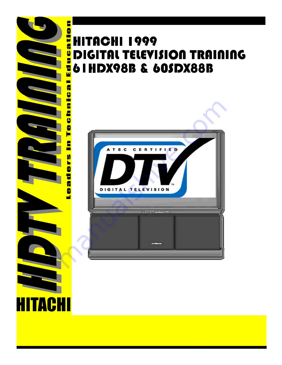
This training package is geared specifically to the 61HDX98B HDTV. However, most of 
the material will cross over to the 60SDX88B progressive scan HDTV capable set. The 
necessary understanding that the 60SDX88B requires a Set-Top-Box  to receive SDTV and 
HDTV signals is important. The 60SDX88B does NOT have a DM-1 module. This module  
is built into the 61HDX98B which allows this set to receive all ATSC formats as well as 
Direct TV,  NTSC, SDTV or HDTV. It does not have Component Inputs. 
The 60SDX88B has a built in FLEX  converter that translates any input into either 480P for 
NTSC or SDTV and/or 1080I for HDTV. It does have Component Inputs. 

The Power Supplies are the same for either set.  
The Deflection circuit is very similar between the two sets. 
The Signal PWB is very similar between the two sets, minus the differences mentioned 
above. 
Digital Convergence is the same between the two sets. 
61HDX98B is a DP-85 chassis with a 16X9 aspect screen. 
60SDX88B is a DP-86 chassis with a 3X4 aspect screen. 

SEE DP-86 TRAINING SECTION IN THE BACK OF THE PACKAGE. 

Summary of Contents for 60SDX88B

Page 1: ... this set to receive all ATSC formats as well as Direct TV NTSC SDTV or HDTV It does not have Component Inputs The 60SDX88B has a built in FLEX converter that translates any input into either 480P for NTSC or SDTV and or 1080I for HDTV It does have Component Inputs The Power Supplies are the same for either set The Deflection circuit is very similar between the two sets The Signal PWB is very simi...

Page 2: ...UT DOWN Circuit Diagram 02 02 Digital Circuit Power Supply Visual Trouble Shooting LED s Diagram 02 03 Digital Circuit Power Supply Distribution Diagram 02 04 Deflection and High Voltage Power Supply SHUT DOWN Block Diagram 02 05 Deflection and High Voltage Power Supply SHUT DOWN Circuit Diagram 02 06 Deflection Power Supply Visual Trouble Shooting LED s Diagram 02 07 Deflection Power Supply Distr...

Page 3: ...stment 08 11 Beam Alignment Adjustment 08 12 Centering Magnet and Beam Shape Magnet Identifications 08 13 Static Centering and Center Adjustment 08 14 Horizontal Blanking Phase Adjustment 08 15 Horizontal Vertical Size Adjustment 08 16 Trapezoid Distortion Adjustment 08 17 Side Pincushion Distortion Adjustment 08 18 Beam Form Adjustment 08 19 Optical System Alignment Lens 08 20 Blue Defocus Adjust...

Page 4: ...ustments Needed 08 40 Accessing Digital Convergence Error Codes 08 41 Adjustments Continued Memory Initialization Procedure 08 42 9 TROUBLE SHOOTING No Raster No Power 09 01 A and B No Relay Click Def Red LED Blinking 09 02 C and R No Red LED B 09 03 D E and F All LED s going off at the same time Def and Power PWB 09 04 G One LED going off a little before the others Dig and Sig Power PWB 09 05 DM ...

Page 5: ... This supply only operates when the set is turned ON When the ON command is received from the DM 1 module relay S 901 energizes and delivers AC to the main bridge rectifier D903 located on the Sub Power Supply PWB This supplies power primarily to the Deflection circuit for the collector of the High Voltage generation circuit and the collector of the Deflection Output transistor Also the Convergenc...

Page 6: ...Out Convergence Vertical Vertical M13 DCU Heater To Signal Block POWER SUB P W B DP85 POWER SUPPLY BLOCK DIAGRAM Fuse 130V Reg 220V 28V 28V 13V Reg 13V Sw Reg 5V Reg 6 3V AC108 132V 60Hz AC Inlet Type To Deflection Block Page 01 02 POWER DEFLECTION P W B 33VS Reg 5V Sw Reg 28V 21V Power Fail L NB Sw Reg A12V Sw Reg 9V Sw Reg TV9V 5V Sw Reg TV5V 3 3V Sw Reg 3 3V Sw Reg HVcc 12V A12V 5V Reg TV9V DCU...

Page 7: ...ATSC formats NTSC Receives the Terrestrial Signal and route it to the NTSC Tuner The NTSC signal is routed out of this block on the line labeled Composite Video to the Signal Selec tor IC which selects the appropriate signal accord ing to the consumer s choice Either Tuner AVX1 2 or 3 and or S In 1 2 or 3 The NTSC audio IF signal is routed to the MTS STEREO DECODER SPLITTER The splitter routes the...

Page 8: ...om the ARM TRANSPORT or the block A Ds AUDIO which is the NTSC audio processed by the Pro Logic decoding circuit labeled as 5 1 Front Left Front Right Center Rear Left and Rear Right Sub Woofer audio also called LFE Then this block processes the signal and outputs all audio to the Audio D As AUDIO D As This block is the Digital to Analog converter which con verts the digital audio signal sent to i...

Page 9: ...TSC UPCONVERSION OSD YUV D As SRAM A D s AUDIO EEROM AUDIO D A s SD A V MODEM Phone SD Satellite Card DM 1 Module Satellite RF Out PinP Tuner Cable Terrestrial L R Composite Video 1HYIQ From Main Micro L R LS RS C LFE L R Data Address Handshake 5 1 Audio DP85 FRONT END BLOCK From Main Micro 2 14YUV YIQ 2 14 HYPBPR Page 01 05 VSB IR from Ft Panel Dimmer AD Key In To 2H Video Circuit Digital ...

Page 10: ...AUDIO VIDEO SELECTOR TA8851BN This is the selector IC Dependant upon the customer s viewing preference the DM 1 will communicate via I2C bus communications and select the NTSC signal which is sent to the demodulator The demodulator prepares the NTSC signal for the DM 1 module This IC selects the following inputs Main tuner Video One Two or Three S In One Two or Three PinP Video and Audio outputs T...

Page 11: ...ut PWB C Video Main R L Audio Main Selected L R NTSC Main Audio Video 4 V4 S4 L R4 PinP Video to PinP Unit Video D YC To 3DYC 9V V1 S1 L R1 V2 S2 L R2 V3 S3 L R3 Video One In Video Two In Video Three In DM 1 I F B4558 I2C AUDIO VIDEO SELECTOR TA8851BN PinP Tuner U001 RF from DM 1 VT 33V Lock Clock Data Enable 5V 9V PinP Video Mono ...

Page 12: ... This will expand the picture side ways and fill the screen However the picture will be non linear Smooth Wide This will keep the center of the pic ture linear and stretch the outside edges to fill the screen With the four choices above the DM 1 module controls the signal for 3 of them Normal Fill and Full However during Smooth Wide the deflection circuit is switched to perform the stretching of t...

Page 13: ... are utilized by the Micro processor for Service OSD positioning HV BLK PH Output during Service Adjustment and in the NTSC normal mode This picture doesn t fill the screen The areas on the side of the picture are called Side Panels This can be adjusted The HV BLK PH controls the timing of the side panel OSD outputs SIDE PANEL APL FROM 2H VIDEO PWB Input the Microprocessor receives a pulse created...

Page 14: ...ervice Menu HBlk S Wide Cut Off D Size Magic Sw Closed Cap Data MEMORY I2 C I2 C VIDEO CHROMA DEMOD 3D Y C Unit PinP Unit Sync Det Sync Det DM 1 I F OSD MIX Digital OSD Busy OSD RGB Ys OSD RGB Ys V Sync I2C Y C Y PinP Video Y C PinP Video from Selector IC 1 H Composite Sync 1HYIQ Main Video from Selector IC YIQ YIQ Mix Clamp AD8056 CCD Video Main CCD Video PinP H BLK PH HV BLK Side Panel APL from ...

Page 15: ...eparation OSD RGB from either the DCU or the Slave Microprocessor is input here Remember that the OSD for Customer usage such as the Channel numbers clock Main Menu etc is generated by the DM 1 Mod ule Also ABL controls the brightness and Contrast as well as the color level at this chip The Velocity modulation control signal is produced from the Rainforest IC This signal is a representative of the...

Page 16: ...5 CHASSIS 2H VIDEO P W B Page 01 12 YUV RGB 9V RGB APL DETECT HV Blk Gen HV Blk HBLK PH 9V DM 1 I F CLAMP GEN 5V 5V 2 14 HV SYNC 2 14 HV SYNC SPANEL Side Panel APL 2 14 SYNC 5V Clamp H V Blk VM YUV YIQ YPBPR Y Clamp YUV YIQ Y PB PR 2 14 HV SYNC OSD RGB ABL I2 C ...

Page 17: ...conditions such as Magic Focus Sensor Initializa tion Data Storage etc Busy notifies the sub Microprocessor I901 which in turn notifies the DM 1 module that the DCU has en tered the DCAM During this time the DM 1 module ignores the remote control commands MAGIC SW When the customer presses the Magic Focus button on the front of the set it produces a command for the DCU to begin the Magic Focus pro...

Page 18: ...R I702 on the Sub Deflection PWB generates the Verti cal Saw signal This signal is controlled by several factors The Sync Processor detection and I2C data communication DIST CONTROL Distortion control is another signal produce by I702 and sent to the Side Pin cushion circuit These com pensation parabolic wave forms are combined with the horizontal circuit to compensate for Side pincushion errors H...

Page 19: ...rovided by the Deflection circuit and I702 on the Sub Deflec tion PWB and impresses these wave forms onto the static DC voltage use for focus This keeps the beam as sharp or focused as possible in the corners of the screen HIGH VOLTAGE REGULATION DETECTOR This circuit monitors a feed back voltage produced from the High Voltage Flyback transformer and routes an output signal to two circuits 1 A sam...

Page 20: ...SOR DISTRIBUTION PHOTO SENSOR SERVICE SWITCH CONV OUT Focus 9KV Screen 700V ABL 6 8 8 DIGITAL CONV UNIT B 130V 34v 34v 6 HV Parabola 1100V Vcp 26V 26V S Wide S Wide D Size Magic SW V Blk H Blk HV Blk Dig RGB Busy IR H Blk V Parabola Saw Size Regulation Control VERTICAL RAMP GEN Diode Modulator To Deflection Yokes To Deflection Yokes 32Kv HV Focus 12Kv 3 3 DF Out Retrace Pulse HDT T752 Cut Off I 2 ...

Page 21: ...REEN FOCUS CONV VIDEO OUTPUT AMP CPT P W B G VIDEO OUTPUT AMP CPT P W B B Def Yokes 30KV HV R G B Beam Shape Beam Alignment Focus VM Coil Deflection and Convergence Yokes Page 01 17 DP 85 CRT PWB BLOCK DIAGRAM RGB VM 220V 12V 220V 12V 220V 12V 220V 26V ...

Page 22: ... 9V 9V From Audio Video Selector IC 9V 9V PinP L R From Selector IC AUDIO OUTPUT SECTION DP 85 CHASSIS To Headphone Jack L R From DM 1 9V HL R HL R I2 C 9V L R RL RR PinP L R L R FL FR L R C LFE 9V L R C 9V LS RS Clock Data RL RR HP L R LFE C L R I2C Clock Data 9V Page 01 18 I2C TL TR TL TR FR Ext Out FL Ext Out Fixed Vari Out L R FL R 26V Sub Woofer FR to Spk FL L R LS RS C LFE 21V 28V ...

Page 23: ...1 MODULE Rear Panel 1 ANT B ANT A L VIDEO MONO AUDIO AUDIO AUDIO MONO VIDEO VIDEO INPUT 1 INPUT 2 L R S VIDEO S VIDEO L R L R L R R TRANSMITTER OUT R L R L FIX VARIABLE OUT INT EXT FRONT SPEAKER 8 ONLY REAR SPEAKER 8 ONLY LFE SUB WOOFER OUT INPUT 3 MONO Page 01 19 AC 3 Jack ...

Page 24: ...ed Cropped DP 85 CHASSIS 4 MODES TO DISPLAY A 4x3 IMAGE ON 16X9 DISPLAY DM 1 Module controls the video content for Normal Full and Fill modes while the deflection circuit is manipulated for the Smooth Wide mode NORMAL MODE 4x3 FULL MODE 4x3 SMOOTH WIDE MODE 4x3 Full Mode 4X3 Stretched to fit Non Linear Normal Mode 4X3 with Black Mask Linear Fill Mode 4X3 Cropped Linear Smooth Wide Mode 4X3 Center ...

Page 25: ...K Page 02 01 I905 Photocoupler I901 ShutDown Pin 7 on Power Supply Driver Output IC 7 3 2 Shut Down SCR 5V Short Det 3 3V Short Det 9V Short Det 5V Loss Det 3 3Vs Too Hi Det 5V Too Hi Det 5Vs Too Hi Det 9V Too Hi Det 12VS Too Hi Det D3 3V Too Hi Det ...

Page 26: ...R976 TV 5V Short Det TV 9V Short Det 5V Loss Det 5VS 5VS B E C Power 5 PQS1 Q914 E C B Off On Off On Off On No Start Up B Off Normal Glowing Blinks during Shutdown because of the internal current draw 15 1V 22 5V pin 5 I901 DIGITAL SIGNAL POWER SUPPLY SHUT DOWN Active High 5 R907 R908 D964 1 2 AC In D905 Run B Start Up B TV 5V Too Hi Det 5V 3 3Vs D934 3 3V Too Hi Det D974 TV 9V Too Hi Det 9V D975 ...

Page 27: ...io F R 28V R956 12VS R939 R965 5VS R966 5VS DP 85 CHASSIS L E D VISUAL TROUBLE DETECTION DIODES SUB POWER PWB DIGITAL POWER SUPPLY 10 GREEN L E D s and 1 RED L E D 11 Total L E Ds for visual trouble sensing observation 3 1 2 Vcc ALL GREEN L E D s 12 Shut Down Inputs Start Up or Run 24 2V 1 9V 24 2V 1 9V Audio Center 21V LNB Power 13V 19V R969 3 3VS R972 D3 3V Page 02 03 D947 D920 D930 D971 D919 D9...

Page 28: ...D 33VS 33V Audio 21V STAND BY 12V CENTER 21V D920 C21 D925 4V Audio 28V AC Plug Live Cold AC Input Noise Filter L901 2 3 Rectifier D901 Protector E992 7K AC Clock I906 RELAY S901 To Deflection Power Supply Protection Block AC Clock 60Hz TV Main ON OFF ON LO OFF Hi D Regulator TV5V I914 Regulator TV9V I908 Regulator 12 I907 5V D971 TV5V ZD ZD 9V 12VS D936 14 7V D928 12V D930 TV9V D925 4V D975 10 8V...

Page 29: ...river Output IC 220V Short Det Heater Short Det 13V Short Det 28V Short Det DP23 DP34 Heater Loss Det Excessive High Voltage Det Flyback Excessive Current Det Side Pin Failure High Det Side Pin Failure Low Det High Voltage Stability Too High Det Deflection Transformer Failure Det DP25 X RAY PROTECT QP06 Q754 Deflection B 130V Excessive Voltage Det Deflection B 130V Excessive Current Det ...

Page 30: ...P41 RP40 13V DP32 DP33 RP42 Heater from Def Power Supply Goes to CRT s DP36 DP37 220V DP35 Heater DP30 13V DP31 28V DP11 CP16 DP17 DP18 13 TP91 Deflection B 130V Excessive Voltage Det Deflection B 130V QP04 RP31 0 47 Deflection B 130V Excessive Current Det QH03 RH23 1 2 9 Flyback TH01 Deflection Flyback Excessive Current Det 10 5 Heater DH31 DH24 DH25 DH26 QH07 DH30 QH06 D754 D753 Q754 1 6 7 8 Def...

Page 31: ...1 B On Bright Shutdown 28V DP 85 CHASSIS L E D VISUAL TROUBLE DETECTION DIODES DEFLECTION PWB 5 GREEN L E D s and 1 RED L E D 6 Total L E Ds for visual trouble sensing observation 3 1 2 Vcc ALL GREEN L E D s 16 Shut Down Inputs Start Up or Run 24 2V 1 9V 24 2V 1 9V 130V Deflection B Page 02 07 RP23 13V RP46 M28V M13V RP26 RP38 RP39 RP37 DP15 DP21 DP16 DP22 DP20 DP06 ...

Page 32: ...Switching Transformer TP91 Protector EP91 4K Switching Control IP01 Feedback IP05 Protect IP06 Voltage Control 130V IP04 Protector SCR QP05 DP06 Protect Red LED HVcc Switch QP08 HVcc 12V Power On Off DP 85 Deflection Circuit Protection Protect In Over Voltage Detector Short Circuit Detector D D D D D D D ZD ZD ZD ZD Deflection 130V Conver 28V Conver 28V Vert 13V Vert HVcc 13V Heater 6 3V DP22 130V...

Page 33: ...702 1 I701 5V Reg 1 23 3 DVcc VRef In I703 Comp 8 Power ON Driver Relay Driver DP 85 DEFLECTION Vcc PRODUCTION CIRCUIT Page 02 09 Other Power On Off Circuits 13V RP66 From IP03 13V Reg PQD2 5 5 DP41 Start Up Power Run Power DEFLECTION PWB SUB POWER PWB SIGNAL PWB SUB DEFLECTION PWB From I907 A12V Reg A12V or STBY 12V ...

Page 34: ...SD2 6 To I001 OSD Position To PinP Unit H Blk 9 To Convergence Circuit To Sweep Loss Det Circuit IH01 1 A1 Q1 12 IH02 10 Osc 7 E r r o r 13 Clamp 12 14 1 Drive 9 10 High Voltage TH01 QH08 QH01 QH09 QH10 130V V2 12 QH05 QH04 FBP In Ref V QH06 HV Sample too High X Ray Protect DP 85 SERIES CHASSIS HORIZONTAL DRIVE CIRCUIT Page 03 01 To Side Pin Circuit To Dynamic Focus To Deflection Loss To X Ray Pro...

Page 35: ...n S 1 In 11 S Y2 S C2 V2 13 15 S 2 In 17 PST1 Cout1 3DYC Comb Filter PCX Comp S Y S C 3DY 3DC Q034 I008 21 22 6 40 Q041 Q040 I011 3 2 1 I010 3 2 1 R Y Out Y Out I009 3 2 1 DM1 PWB ATSC NTSC Q039 14 12 10 PMS2 V Cr U Cb Y IX01 Rainforest IC 53 IX02 3 2 1 QX01 3 5 1 PMZ V PR U PB Y Y IX03 3 2 1 3 2 1 QX03 QX05 51 V PR 52 U PB 41 42 43 Y V PR U PB QX23 QX28 QX33 3 5 1 PZC B G R Signal Sub PWB To CRT ...

Page 36: ... 16 To Anodes ABL To QH01 Collector of Horz Output Transistor Signal Sub PWB Deflection PWB Clamp ABL Pull Up Resistors As Brightness goes Up ABL Voltage goes Down Inverse Proportional Current Path QX14 RX79 CX21 RX81 9 27 See uP Data Signal Path Page 04 02 DH33 RH23 RH22 QH03 CH18 See XRay Protect RH56 Deflection B 130V V1 PSD2 1 DX01 CX20 CX24 PSZ1 SCL2 SCL2 17 28 TH01 ...

Page 37: ...2 QN01 IH02 13 Error Out 12 Error In 1 14 Reference Feed Back 7 Drive High Voltage Driver IC Q610 PSD 2 2 3 Cut Off Stops High Voltage Drive Signals From being produced during 13V start up 10V P P RN16 DN07 0V RN17 CN06 DN08 RN18 ACK 5V 8 57V 8 57V RN14 From I906 Pin 3 AC Photo Coupler 9 72V QN06 RN17 I601 4 Non Invert Input 5 Invert Input Q601 Q602 Vertical Output IC R605 R602 Vert SAW R604 5V Sp...

Page 38: ... 43 SCL1 SDA1 PMT1 1 PinP Tuner 20 Mono PinP 1 3 PinP Audio In Left Select Right Select DM 1 Digital Control Center PSU1 PAS2 Audio Output PWB 4 6 I402 2 2 Center Spk Center Audio Output IC LFE SW Front Left Spk Front Right Spk Int Spk Ext Spk External Left Spk Jack External Right Spk Jack 1 PSP1 PCL 3 SS01 8 10 14 16 AVX 1 AVX 2 51 49 AVX 3 1 2 Surround PWB 2 of 2 12 I403 2 4 12 7 Rear Output IC ...

Page 39: ...er 32 1 IS04 5 6 7 3 2 1 R Ft Center L Ft Center ISO1 Ft Trans mitter Audio Cont 32 1 10 23 30 28 IG01 3 2 1 5 6 7 R Ft L Ft Graphic EQ 15 18 Rear Left 1 7 IS11 2 3 1 6 5 7 20 13 PHP 1 3 To Head Phone Jacks HPL HPR PAS2 To Audio Output PWB 2 1 R L Left Front 15 18 Right Front 13 20 QS03 QS04 QS01 QS12 Transmitter Out Jacks 6 4 Center LFE Sw 18 13 20 QS07 QS08 QS09 QS10 Fixed Vari Audio Out L Fixed...

Page 40: ...97 Micro Processor V MUTE RO52 14 IX01 25 DX05 FBP In SPOT MUTE Q022 R145 R098 2H Video PWB V Mute Mute 2 Signal PWB RO10 16 15 Surround PWB Page 05 03 A12V 56 10 A5V Spot RO51 RO92 9V V Mute 7 CRT PWBs 7 Spot HVBlk Rainforest Mute Mute 2 V Mute 2 Grounds Bias to Q8A3 Q853 Q803 Horizontal Vertical Sweep Loss Det AC Loss Det From Deflection PWB From QZ13 and IZ07 V Mute 2 PSZ2 PZC PZC PSU1 PSD2 ...

Page 41: ...e Left DS30 QS14 CS83 CS82 DS28 DS29 LFE Sub Woofer DP 85 MUTE CIRCUIT DIAGRAM SURROUND PWB Also see Audio and Video Mute Circuit Diagram Also see Mute Circuit Diagram Audio Output PWB PSA1 4 5 VMUTE2 MUTE2 MUTE VMUTE Transmiter Right Out Transmiter Left Out Fixed Variable Right Out Fixed Variable Left Out LFE Sub Woofer Out See Audio Output Mute Circuit Diagram Page 05 04 RSC6 RSC4 RSC5 RSC7 RSF2...

Page 42: ... D415 R418 C409 R415 VMUTE 4 D424 Q409 R448 R444 C440 D425 Rear Right I403 C442 Q410 R449 R413 C402 Rear Left C404 R446 R447 Q411 R452 C448 D426 D427 R450 C447 R451 Rear Spk Off 3 D419 Center Audio Output IC I402 Q406 R449 R431 C423 Rear Left C425 R433 Q407 R438 C430 D420 D421 R436 C429 R437 D418 Center Spk Off 2 Front Right Front Left Mute Rear Right Rear Left Mute Center Mute Page 05 05 Front Au...

Page 43: ...Convergence Yokes 5V 5V 5V SRAM HBlk D Size 5V Digital V Sync OSD R BUSY IR In OSDG ADJ OSDB STAT DCAM Digital Convergence Mode QK0 7 QK0 6 QK0 8 I001 Main Up PSD4 4 5 6 7 3 2 1 PFS I501 Rainforest PZC 5 3 1 41 42 43 33 34 35 Q013 4 5 1 2 10 D H OSD Sel 9 54 42 43 OSD B OSD G OSD R Adj B Adj G Adj R Adj B Adj G Adj R Dig OSD B Dig OSD G Dig OSD R PSZ1 13 12 11 To CRTs B G R OSD B OSD G OSD R I105 ...

Page 44: ...rgence alignment data is STORED for the following 4 Smooth Wide Mode mode MAGIC FOCUS AUTO DIGITAL CONVERGENCE Customer s function When the customer presses the magic focus button it will be necessary for them to perform Magic Focus in similar fashion Pressing Magic Focus will correct any one of the following Modes 1 Normal mode 2 Full mode 3 Fill mode Magic Focus must also be pressed for 4 Smooth...

Page 45: ...104 104 114 95 762 Page 06 03 DIGITAL CONVERGENCE OVERLAY DIMENSIONS B R H SIZE V SIZE Centering Offset 1350 41 49 97 97 97 97 97 97 49 41 20 88 113 4 20 88 113 4 113 4 113 4 113 4 113 4 113 4 113 4 762 DIGITAL CONVERGENCE OVERLAY FULL MODE DIGITAL CONVERGENCE OVERLAY SMOOTH MODE Part Number H312182A Part Number H312221 ...

Page 46: ...SER GREEN adjust Digital Cursor Blinks GREEN 3x3 adjustment mode Press 5 times can only be entered when R A M is cleared CURSOR KEYS ADJUSTMENT Adjust the selected color at the current stopping position Up Down Left Right MOVES DIGITAL CURSOR Moves Adjustment Point 2 Up 4 Left 5 Down 6 Right INPUT BLUE adjust Digital Cursor Blinks BLUE 13 x 9 adjustment mode Press 5 times 0 RED adjust Digital Curs...

Page 47: ... to IZ06 controlling the phase of the Side Pannel pulses High 12 P50 MAIN PinP Outputs a control signal to I012 for selection of Main Sync or PinP Sync High 13 P01 SCL Clock for the EEPROM Data 14 P47 Smooth Wide Outputs control signal to Q753 and I751 to switch deflection to Smooth Wide High 15 P02 SDA Data for the EEPROM Data 16 P51 4 3 When Fill Full or Smooth Wide mode is selected in NTSC outp...

Page 48: ...L1 SCL Clock for the PinP Front audio controller and AV switch IC Data 48 P65 Data Data to control the Front L R and Center Graphic Equalizer Data 49 P10 KEYIN Not Used n a 50 P20 KEYIN Notification of the OEM in which the chassis is used Diode D002 identifies it as Hitachi by feeding back Key Out2 pulses from pin 38 Data 53 P20 Power ON OFF When the DM 1 Module instructs the Slave Micro to turn O...

Page 49: ...EL Det P16 N A P BLK P66 V STOP P26 V MUTE P61 Power On Off P20 Auto Convergence SW P67 Rx SOUT SIN Tx SCLK Clock INT1 Request PWM4 P47 P27 AD2 AD3 TIM2 P43 Arm Up DP 85 SYSTEM CONTROL PORT DESCRIPTION Page 07 03 I001 10 8 7 5 6 14 11 19 23 17 21 44 53 56 9 46 40 59 60 57 55 62 63 64 61 1 2 58 16 12 CVIN 28 Reset CVIN 36 37 38 39 41 3 49 50 13 15 47 43 45 42 48 54 IG11 IG02 I702 U301 IS03 IS02 I30...

Page 50: ...04 6 4 5 3 PMS2 DM 1 MODULE 45 42 SCL2 SDA2 47 43 SCL1 SDA1 1 2 PSD1 9 8 PDD2 IOO2 EEPROM 5 6 SDA3 SCL3 I702 Sweep Control 4 3 SCL2 SDA2 SCL2 SDA2 3D Y C UNIT PCX SCL2 SDA2 PinP UNIT U002 3 2 1 2 5 4 PSU1 17 16 7 6 54 48 GEQ CLOCK GEQ DATA 13 12 Surround PWB IS01 Front Transmit Audio Control SCL1 26 27 SDA1 17 16 17 16 17 16 IS03 Rear Headphone Audio Control IS02 Center LFE Audio Control IG11 Cent...

Page 51: ...apezoid FULL NTSC CLEAR 14 Side Pin FULL NTSC CLEAR 15 Horz Size Adj SMOOTH NTSC CLEAR 16 Vertical Size Adjust SMOOTH NTSC CLEAR 17 Trapezoid SMOOTH NTSC DCU Grid CLEAR 18 Side Pin SMOOTH NTSC CLEAR 19 Beam Form NORMAL NTSC 20 Lens Focus Adjust FULL NTSC 21 Static Focus Adjust FULL NTSC 22 Blue Defocus FULL NTSC 23 White Balance Adjustment FULL NTSC 24 Sub Brightness Adjustment FULL NTSC Color Bar...

Page 52: ...63 12 PinP Unit 16 CONT Contrast CENTER 0 127 63 UNI COLOR 18dB to 0dB TA1276AN 17 CONT T Contrast Center offset Theater Mode 0 127 63 UNI COLOR 18dB to 0dB TA1276AN 18 BRT YIQ Brightness YIQ TA1276AN 19 BRT T Black Level Center offset Theater Mode 0 255 127 40IRE to 40IRE TA1276AN 20 C YIQ Color Center NTSC YIQ 0 127 63 Color Min 20dB to 4dB TA1276AN 21 C 170 Color Center SMPTE 170M 0 127 63 TA12...

Page 53: ...31 15 uPc1885 45 Don t Care 46 Don t Care 47 Don t Care 48 RGBBRT RGB Black Level Digital Convergence 0 127 63 4dB to 0dB to 3dB TA1276AN 49 RGBCNT RGB Contrast Digital Convergence 0 127 90 18dB to 0dB TA1276AN 50 WPSL White Peak Suppressing Level WPSL 0 1 1 0 130IRE 1 110IRE TA1276AN 51 HIBRT High Bright Color HIBRT 0 1 0 0 Off 1 On 52 CGAMMA Color Gamma Correction Point 0 3 0 0 Off 1 O 2Vp p 2 0...

Page 54: ... 0ns 3 20ns TA1276AN 72 PIPVOL PinP Volume 73 APC NT APACON PEAK f0 NTSC 0 7 7 0 Off 1 4MHz 2 3 3MHz 4 2 5MHz TA1276AN 74 APC SD APACON PEAK f0 SDTV 0 7 6 5 Off 6 13MHz 7 10MHz 8 8MHz TA1276AN 75 APC HD APACON PEAK f0 HDTV 0 7 5 TA1276AN 76 SVMLMT Velocity Modulation Limit 0 1 0 0 Parabola Modulation OFF 1 On TA1276AN 77 DCR PO D C Restoration Point 0 7 0 0 0 to 7 42 TA1276AN 78 DCR RA D C Restora...

Page 55: ...inP Unit 99 CLR P Color PinP 0 255 121 PinP Unit 100 TNT NT Tint Main Picture NTSC 0 127 56 TA1270AF 101 CNT NT Contrast Main Picture NTSC 0 31 27 TA1270AF 102 CLR NT Color Main Picture NTSC 0 31 12 TA1270AF 103 CCD D CCD Data Slice Line 00E0H 0 255 17 104 CCD S CCD Start Bit Position 00E1H 0 255 210 105 CCD W CCD Window Position 00E2 0 255 41 106 CCD C CCD Clock Line Counter 00E6H 0 255 5 107 CCD...

Page 56: ... Beam Alignment magnets 6 Focus Block Assembly RED GREEN BLUE Also Drive Adjustment controls for RED GREEN BLUE 1 Centering magnet RED 2 Centering magnet GREEN 3 Centering magnet BLUE 4 Beam Form Magnets DP 85 MAGNETS Adjustment Points RED CRT GREEN CRT BLUE CRT 2 1 3 4 5 6 4 4 5 5 FRONT ...

Page 57: ... Blue C R T Pre set between the 1 2 o c l o c k and 2 o clock position 2 SCREEN VR ON FOCUS PACK Pre Set fully counter clockwise 3 Focus VR on focus pack Pre Set fully clockwise PRE HEAT RUN CONDITION DP 85 Series Chassis 12 2 DRIVE VR SCREEN VR FOCUS VR Projection Front View R G B R G B Screen VR Focus VR FOCUS PACK RED CRT GREEN CRT BLUE CRT ...

Page 58: ...hat particular color is barely visible 4 Repeat for the other t w o colors FOCUS ADJUSTMENT 1 Short the 2pin sub miniature connector on the C R T P W B TS to remove any color not being adjusted and adjust one color at a time The adjustment order of R G and B is just an example 2 Adjust the Focus VR for Red until maximum Focus is achieved 3 Repeat for Blue and Green 4 To Return to Service Menu pres...

Page 59: ...dicated in the chart until the data matches the values indicated in the chart Exiting Adjustment Mode 6 Press Help key on remote control 7 Press SWAP key TWICE to store the information 8 When Green dots are displayed press the 8 key on remote 9 Press the SERVICE ONLY switch to return to normal mode SMOOTH Mode Adjustment Mode 1 0 Change the Display Format to SMOOTH WIDE Mode 1 1 Repeat steps 3 thr...

Page 60: ...nt menu and select Item 4 HPOS F and adjust the data so that the center of Video matches the location of the Digital Cross hatch pattern noted in step 4 6 Write do w n the data value 7 Exit from the I2 C M e n u SMOOTH WIDE Mode Adjustment 1 Receive any NT S C crosshair signal 2 Screen Format is SMOOTH 3 Press the SERVICE ONLY switch on the deflection P W B and display the Digital C o n vergence C...

Page 61: ...press the POWER but ton The Service Only switch is on the De flection P W B Adjustment Procedure GREEN 1 A p ply covers to the RED and BLUE lenses or short the 2P Sub M i ni connector TS on each CRT P W B to pro duce only GREEN 2 Turn the Green deflec tion yoke and adjust the TILT until the green is level 2mm tolerance See diagram RED 1 Remove cover fro m RED C R T and align RED with GREEN 2 1mm t...

Page 62: ... does move repeat steps 2 through 6 8 Conduct beam alignment for Red and Blue in the same way 9 Red R focus on focus pack 1 0 Blue B focus on focus pack 1 1 Upon completion of adjust ment place a small amount of white paint on the beam alignment mag nets to assure they don t move If available BEAM SHAPE Preparation for adjustment IMPORTANT Screen format should be NORMAL 1 The beam alignment should...

Page 63: ...ly made of metal and is located up against the back side of the yoke assembly Not down on the neck of the CRT Figure 2 shows the Beam Form and Alignment magnet This magnet is normally made of plastic and is located close to the CRT PWB on the neck of the CRT NO ADJUSTMENT ZERO FIELD SPACER PICTURE TUBE SIDE 4 POLE BEAM SHAPE CORRECTION MAGNET 2 POLE BEAM ALIGNMENT MAGNET ADJUSTMENT TABS BEAM FORM ...

Page 64: ... Digital Convergence adjustment procedure 2 Apply the Digital convergence overlay 3 Press the Menu button on the remote to turn off Red and Blue 4 Adjust the centering magnets for G on the back side of the Deflection Yoke and align the center of the G Crosshatch to the center of the overlay 5 Select Red adjustment Mode 0 on the remote control 6 Adjust the R centering magnet and align the center of...

Page 65: ...wn button together to display Service Adj Mode 2 Choose item 7 HSIZE F with the remote up do w n keys and NOTE the current data value Reduce to mini m u m 3 Display only Green by shorting the sub mini 2pin connector on the Red and Blue CRT P W B 4 Select item 3 HBLKPH with the remote up do w n keys 5 Adjust until l2 is equal with l1 See figure below 6 Choose item 7 HSIZE F with remote up down keys...

Page 66: ...overlay 7 Press the MENU key on remote control to exit Ser vice Menu HORIZONTAL SIZE Display Mode FULL or SMOOTH WIDE as Depicted 1 Enter I2 C Service Mode and choose Item 7 HSIZ F FOR SMOOTH WIDE MODE Smooth Wide select Item 12 HSIZ S 2 Adjust data value using left and right cursor until the 5th line from center matches the lines indicated on the left and right hand side of the overla y 3 Press t...

Page 67: ...C signal and Display Format is set to FULL mode 2 Go to I2 C Service Adj m o d e Press the TV SAT and Channel Down button together to display Service Adj Mode 3 Choose item 6 TRAP F with the remote up do w n keys 4 Adjust Trapezoid as sho w n 5 Press MENU key on re mote to exit Service Menu Adjustment procedure SMOOTH WIDE MODE 1 Receive any NT S C signal and Display Format is set to SMOOTH WIDE m...

Page 68: ...ignal and screen format is set to FULL mode 2 Go to I2 C Service Adj m o d e Press the TV SAT and Channel Down button together to display Service Adj Mode 3 Choose item 5 SPIN F with the remote up do w n keys 4 Adjust Side Pin as sho w n 5 Press the MENU key on remote to exit Service A d justment Mode Adjustment procedure SMOOTH MODE 1 Receive any NT S C signal and screen format is set to S M O O ...

Page 69: ...ctors on Red and Blue C R T PWB to project only the Green beam 3 Turn the green static focu s VR fully clockwise 4 M a k e the dot at the screen center a true circle as sho w n in Figure 2 using the 4 Pole magnet sho w n in Figure 1 5 Also adjust the Red and Blue CRT beam shapes ac cording to the steps 1 to 3 6 A f t er the adjustment is c o m pleted return R G and B static VRs to the Best Fo cus ...

Page 70: ... that the lens cyl inder can be turned Be careful not to loosen the screw too much as this may cause movement of the lens cylinder when tightening 3 Rotate the cylinder back and forth to obtain the best focus point while observ ing the Cross Hatch Observe the center of the screen Hint Located just belo w the screen are the two cen ter speakers These speak ers are mounted on t w o wooden panels Rem...

Page 71: ...should be FULL mode Adjustment Procedure NORMAL MODE 1 Receive any NT S C cross hatch signal 2 Screen Format is FULL 3 Turn the B FOCUS VR fully clockwise 4 Adjust BLUE defocus a c cording to the follo w i n g specifications 1mm on each side equaling 2mm total See figure Blue Defocus Sticking Out Center of Blue crosshatch line R G B R G B Screen VR Focus VR FOCUS PACK Blue Focus VR on FOCUS PACK ...

Page 72: ...procedure 1 Go to I2 C A D J Mode With power ON press DTV SAT and Cursor Down buttons at the same time Service Menu is displayed 2 C h o o s e S E R VI CE item Number 1 of I2 C A D J M o d e Select ON by Cur sor Right and the Vertical will collapses 3 Gradually turn the screen adjustment VRs red green blue clockwise and set them where the red green and blue lines are equal and just barely visible ...

Page 73: ...nt 1 Start adjustment 20 min utes or more after the p o w er is turned on 2 Receive a tuner signal 3 Set the contrast and color controls to minimum 4 Set the brightness to mini mum position on the dis play 5 The room light should be very lo w ADJUSTMENT PROCEDURE 1 Go to I2 C A D J Mode With power ON press TV SAT and Cursor Down buttons at the same time Service Menu is displayed 2 Adjust Sub Brigh...

Page 74: ... MENU button to exit from the Service M e n u SMOOTH Mode Adjustment 1 Receive any NT S C cross hatch signal 2 Display Format is SMOOTH WIDE mode 3 Enter the I2 C Bus alignment menu and select Item 9 HPOS S 4 Adjust the data using the left and right cursor keys but D O N O T b alance the Left and Right hand side Smooth mode with have a shift due to the D M 1 m o d ule This is normal See fig ure be...

Page 75: ... 5 95 5 95 5 47 8 46 7 26 119 26 95 119 107 107 107 104 104 114 DIGITAL CONVERGENCE OVERLAY SMOOTH MODE 95 762 Red and Blue Centering Offset is necessary to free up memory in the Digital Convergence Unit It is important to offset the Red and Blue centering during Magnet Centering Failure to do so could produce a Memory Overrun error Red Offset 10mm and Blue Offset 30mm for Normal and Smooth Wide M...

Page 76: ... 5 times to access the 3 X 3 Mode NOTE Old ROM data can be restored by pressing the PIP button TWICE The set will be restored to the last condition when data was stored 1 2 3 4 5 6 7 8 9 MUST USE OVERLAY IN THIS MODE Begin with Green in this mode 1 2 3 4 5 6 7 8 9 10 11 12 13 14 15 20 21 22 16 17 18 19 23 24 25 26 27 28 29 30 31 32 33 34 35 5 X 7 MODE 35 stopping positions DIGITAL CONVERGENCE CURS...

Page 77: ...2 113 114 115 116 117 13 X 9 MODE 117 stopping positions Press the INPUT button on the CLU 914MP remote 5 times to activate the 117 stopping positions The raster will blink and the cursor will flash indicating 13 X 9 MODE NOTE This is the normal mode when entering the digital convergence adjustment mode Sometimes during adjustment S Distortion can occur This is when the line has a noticeable wavy ...

Page 78: ...Digital Cursor Blinks GREEN 3x3 adjustment mode Press 5 times can only be entered when R A M is cleared CURSOR KEYS ADJUSTMENT Adjust the selected color at the current stopping position Up Down Left Right MOVES DIGITAL CURSOR Moves Adjustment Point 2 Up 4 Left 5 Down 6 Right INPUT BLUE adjust Digital Cursor Blinks BLUE 13 x 9 adjustment mode Press 5 times 0 RED adjust Digital Cursor Blinks RED 7x5...

Page 79: ...tton then press the POWER Button simultaneously until the set is on When video appears press SERVICE SWITCH again Internal Digital Cross Hatch Signal is projected Service only switch is on the deflection PWB Receive any NTSC signal Crosshair if possible Set SCREEN FORMAT TO FULL mode A l i g n t h e G R B individual center crosses to their respective marks on the Overlay using the Yoke Center Magn...

Page 80: ... Cursor buttons to match the selected Crosshatch red and blue to the green Align Red and Blue static centers Press the Remote MOVE button to exit Static Centering extra lines will disappear Green should already be centered Internal Cross Hatch Signal selected B Extra Lines appear indicating Raster Mode Adjust Color Left Adjust Color Up Adjust Color Down Adjust Color Right Remote FAV CH FAV CH MENU...

Page 81: ... button to project the green tube only Selects GREEN Before Adjustment After Adjustment Moves location of Adjustment Point Intersection of blinking cursor Remote 4 5 6 2 Lines symmetrically aligned at Adjustment Points Cursor blinks at intervals of 3 to indicate the 3X3 Adjustment Mode C Green Only 3X3 Mode 9 Adjustment Points USER Button is used for selecting the 3X3 Adjustment Mode when pressed ...

Page 82: ...o converge the selected color onto green Convergence 3x3 Mode 9 Point Adjustment Red Blue Coarse Alignment Green always projected Selects Blue Crosshatch is yellow when the red and green crosshatches align Crosshatch is cyan when the blue and green crosshatches align Has the Blue 3x3 Convergence Mode been aligned Yes Press Menu Button D No White internal crosshatch should be projected Calculation ...

Page 83: ...INPUT C S 0 9 8 7 6 5 4 Remote Selects the 7X5 mode Press the Remote INFO button to interpolate points in between the adjustment points 35 convergence adjustment points in 7X5 mode E Use the Remote Cursor and 2 4 5 6 buttons to perform convergence point adjustment at every other intersection of the crosshatch Adjust Color Left Adjust Color Up Adjust Color Down Adjust Color Right Remote FAV CH FAV ...

Page 84: ...at every other intersection of the crosshatch Press the Remote INPUT button to select the Blue Convergence Adjustment Mode INPUT C S 0 9 8 7 6 5 4 Remote Perform adjustment at every other intersection Has the Blue 7X5 Convergence Mode been aligned Yes Press Menu Button E White Internal Crosshatch should be projected Cursor Blinks Blue Cursor blinks red at intervals of 2 to indicate the 7x5 mode Se...

Page 85: ...e INPUT C S 0 9 8 7 6 5 4 Remote Selects the 13X9 mode Use the Remote Cursor and 2 4 5 6 buttons to perform convergence point adjustment at every other intersection of the crosshatch 117 convergence adjustment points in 13X9 mode G Press the Remote INFO button to interpolate points in between the adjustment points Adjust Color Left Adjust Color Up Adjust Color Down Adjust Color Right Remote FAV CH...

Page 86: ...f t h e crosshatch Press the Remote INPUT button to select the Blue Convergence Adjustment Mode INPUT C S 0 9 8 7 6 5 4 Remote Perform adjustment at every intersection Has the Blue 13X9 Convergence Mode been aligned Yes Press the Menu Button to Display all colors G White Internal Crosshatch should be projected Cursor Blinks Blue Cursor blinks red indicating the 13X9 mode Selects Blue for adjustmen...

Page 87: ...ust be done after a Write to Rom STORE in order for MAGIC FOCUS to operate If this is not done when the MAGIC FOCUS button is pressed the Static Centering Mode will be entered Return to the Digital Conv Adjustment Mode and Initialize the Magic focus I This screen appears with a series of green dots indicating a successful Write to Rom or Store Note If Red dots appear retry the process If Red dots ...

Page 88: ... Switch to Exit to Normal Mode I MAGIC FOCUS Press the Remote PIP CH button to begin the Initialization Mode Screen projects different light patterns during the Initialization Mode Press the Remote SWAP button once Change the screen format to SMOOTH WIDE mode Install the Smooth Wide Overlay Press the Service Only switch to enter the DCAM Return to D and align to the Overlay After completing NORMAL...

Page 89: ...en Release Button Release Button CENTER ADJUSTMENT Internal crosshatch should appear Internal Crosshair or Center Cross should appear Press MAGIC FOCUS Button to Exit to normal Mode Static or Center alignment is off STATIC ADJUSTMENT STATIC CENTER Center Cross will blink indicating which Color can be adjusted Adjust using the cursor keys on the Remote To select other color press the Menu Button Ce...

Page 90: ...djusted Touch Up complete Convergence Point Adjustment IMPORTANT Begin in FULL mode When adjustment is complete STORE the New DATA by pressing the SWAP button twice Press the Service Only Switch to Exit to Normal mode Press following for Selected Color to Adjust USER Green 0 Red INPUT Blue Press 0 five times to select the 7X5 Mode Press INPUT five times to select the 13X9 Mode Note 3X3 mode can no...

Page 91: ...measure Application Initialize Magic Focus 1 VF Error Replace DCU X X 2 2 Connect 1 1 Darken Outside Light 2 Placing of Sensor 3 Is pattern hitting sensor 4 Check connection and solder bridge of sensor 5 Replace Sensor 6 Replace Sensor PWB 7 Sensor Connector check 8 Replace DCU 9 Adjustment check H V size centering X 3 2 A D Level Same as Error Code 2 X X 4 Over Flow 1 Check the placement 2 Adjust...

Page 92: ...the past Service Adjustment Data will be erased All Service Adjustment Data will be lost EEPROM REPLACEMENT When the EEPROM is replaced new data for the Service I2C will be in volved Before operating the set the EEPROM must be initialized To Initialize the EEPROM 1 If possible write down the data values for all Service Adjustments 2 With Power Off remove the old EEPROM and install the new EEPROM 3...

Page 93: ... Deflection PWB Is Red LED Blinking Protection Deflection PWB 1 Trun OFF Power SW 2 Turn ON again after several minutes and carefull observe ALL green LED s Deflection PWB 1 Trun OFF Power SW 2 Turn ON again after several minutes and carefull observe ALL green LED s Power PWB Is Red LED OFF Protection Deflection PWB Did 5 green LED s turn OFF same Time Deflection PWB Did 5 green LED s turn OFF sam...

Page 94: ...L001 L004 No Signal PWB Is Voltage at pin 6 of I001 AC Clock In 2 5Vdc Signal PWB Check I001 I003 Reset IC X001 Crystal Yes No Signal PWB Check Q015 Q016 I003 Reset IC X001 Crystal Power PWB I906 D909 Deflection PWB Is Voltage at pin 5 of IP01 21V 24V Yes B No Deflection PWB Check DP02 RP05 RP06 CP05 Deflection PWB Signal PWB No Relay Click Heard Deflection PWB Has Protector EP91 blown Yes No Defl...

Page 95: ...5 CHASSIS TROUBLESHOOTING 1 No Raster and No Power Power PWB Check D907 Replace I901 Power PWB Is Voltage at pin 5 of I901 21V 24V C Yes No Power PWB Check I901 R912 R913 R914 Power PWB Power PWB Check I901 D961 Shorts on B Lines Replace E992 Power PWB Has protector E992 blown R Yes All HOT Ground All HOT Ground All HOT Ground All HOT Ground ...

Page 96: ...n PWB Check T751 R754 R755 EP96 LP13 No Power PWB Does raster appear with G and K of Q913 shorted Power PWB Check Q913 Yes E No Power PWB Power PWB Check Q913 I905 D954 D961 I904 Q915 D955 F Deflection PWB Deflection PWB Find which LED is going Dark or OFF Other LED s are going OFF a little latter Deflection PWB DP22 130V Check EP98 DP11 Q777 QH01 TH01 DH11 etc Deflection PWB DP15 13V Check EP94 I...

Page 97: ...k 5VS PMQ1 PMQ2 PMQ3 disconnect Power Check 5VS line Q909 etc Check DM 1 Bright Power Is D928 dark Dark Power D928 is Dark 5VS PMQ1 PMQ2 PMQ3 disconnect Check Standby 12V line Power D927 I907 Signal PWB Q001 I001 etc Check DM 1 Bright Power Is D945 dark Dark Power D945 is Dark 3 3VS PMQ1 PMQ2 PMQ3 disconnect Power Check 3 3VS line I911 D946 etc Check DM 1 Bright Power Is D947 dark Dark Power D947 ...

Page 98: ...output To measure hook scope probe to convenient ground and measure signal The reference for any given signal is the same but 180 degrees out of phase Always consult the schematic for the actual pin number of the desired signal Connecting the ground clip of a grounded scope to the REF line will cause damage to components DP 85 HDTV DM 1 TO CHASSIS INTERFACE 1 3 5 1 3 5 NTSC IN 1H Video 2H PB PMZ L...

Page 99: ...s powers on OSD pre sent but no video 1 Check signal sources 2 Apply ATSC BSS signal check for Link Locked LED inside DM 1 3 If Link LED is on Link Locked check 2H Y H V at PMZ See drawing Functional DM 1 will generate OSD with out a signal source attached Chassis powers on but no OSD Power LED blinks twice when AC Power is applied DM 1 is functional Note New DM 1 modules do NOT blink the power LE...

Page 100: ...Request After checking all the DC voltages between the DM 1 and the Main chassis investigate the Waveforms Check on Connector PMS2 Pin 4 IP Clock Check on Connector PMS2 Pin 6 IP RX Check on Connector PMS2 Pin 5 IP TX Waveform only available during Power On and Off WAVEFORMS FOR DM 1 VIDEO TROUBLESHOOTING See Page 09 06 for DC Voltages Check on Connector PMT1 Pin 1 Video NTSC Check on Connector PM...

Page 101: ...OUBLESHOOTING Continued Check on Connector PMZ Pin 1 Y 2 14 After checking all the DC voltages between the DM 1 and the Main chassis investigate the Waveforms Check on Connector PMZ Pin 3 2H Pr 2 14 Check on Connector PMZ Pin 2 Y Ref Check on Connector PMZ Pin 3 2H Pr 2 14 Check on Connector PMZ Pin 9 V Sync Check on Connector PMZ Pin 5 2H Pb 2 14 Check on Connector PMZ Pin 11 H Sync Check on Conn...

Page 102: ...ff the Collector of Q777 and or Pin 1 of T752 is routed to the Base of Q755 Q755 functions as an Emitter follower and produces the Horizontal Blanking signal from it s Emitter Another signal produced is utilized by the Conver gence section The nega tive 28Volts from the Power supply is sent through T752 and a Pulse is added to it This in turn is routed to the Conver gence output Transistors and is...

Page 103: ...ive signal This signal must be present for the High Voltage section to function This signal is routed to IH01 to be processed into the actual drive signal for the High Voltage section HORIZONTAL WAVEFORMES COMPARED TO H DRIVE The Deflection H Drive signal developed by Q755 See Figure 7 is routed to IH01 pin 1 See Figure 11 The following waveforms give a visual example of the Signal Process as it e...

Page 104: ...r ON command is generated from I001 pin 55 high the power on driver Q007 is turned on A LOW is produced at it s collector and routed through the PQS1 connector pin 3 This low is then routed to the PQD2 connector pin 5 to the base of QP08 turning it ON and supplying 12V to the connector PDD1 pin 1 and 2 This 12V then is routed to I702 pin 1 I701 pin 1 and I703 pin 8 on the sub de flection PWB This ...

Page 105: ...CX Pin 9 09 15 Video Out PinP Tuner U001 Pin 23 09 15 VSAW Out PDD2 Pin 3 09 15 VPARA1 PDD2 Pin 5 09 15 VPARA2 PDD2 Pin 6 09 15 QH08 Base High Voltage Driver 09 15 QH08 Collector High Voltage Driver 09 15 QH10 Emitter High Voltage Driver 09 15 Anode of DH24 Excessive Hi Volt Det 09 15 FBP In IX01 Pin 25 09 15 B Out IX01 Pin 41 09 15 G Out IX01 Pin 41 09 15 R Out IX01 Pin 43 09 15 VSM Out IX01 Pin ...

Page 106: ... Varies DC 4 25 V SCL1 PSU1 Pin 6 Vp p 5 250 V Freq 52 63 kHz DC 4 82 V SDA1 PSU1 Pin7 Vp p 4 969 V Freq 55 56 kHz DC 4 82 V Infrared PFS Pin 2 AC 50 60 I001 Pin 6 Y PinP U002 Pin 5 Vp p 4 875 V Freq Varies DC 4 96 V H Sync I001 Pin 1 Vp p 4 906 V Freq 33 75 kHz DC 4 21 V Vp p 4 875 V Freq 59 97 Hz DC 2 54 V I PinP U002 Pin 6 Vp p 575 0 mV Freq 15 75 kHz DC 3 15 V Vp p 706 2 mV Freq 15 75 kHz DC 3...

Page 107: ... p 2 281 V Freq 59 70 Hz DC 4 99 V 3D Y PCX Pin 9 Vp p 1 406 V Freq 15 75 kHz DC 2 69 V VPARA2 PDD2 Pin 6 Vp p 600 mV Freq 59 70 Hz DC 2 11 V Vp p 12 06 V Freq 33 75 kHz DC 4 52 V Emitter of QH10 B Out IX01 Pin 41 G Out IX01 Pin 42 Vp p 12 0 V Freq 33 78 kHz DC 4 31 V FBP In IX01 Pin 25 Vp p 4 187 V Freq 33 78 kHz DC 1 09 V Vp p 3 172 V Freq 33 78 kHz DC 2 56 V R Out IX01 Pin 43 Vp p 3 219 V Freq ...

Page 108: ...kHz DC 0 02 V 3 58Mhz I008 Pin 3 Vp p 75 0 mV Freq 3 57 MHz DC 3 80 V Vp p 148 4 mV Freq 504 kHz DC 5 88 V Vp p 631 2 V Freq 58 57 kHz DC 0 28 V Vp p 11 0 V Freq 59 97 Hz DC 4 36 V Sync Out I008 Pin 9 Vp p 2 563 V Freq 15 75 kHz DC 2 46 V SMFET I901 Pin 1 Vp p 306 3 V Freq 80 16 kHz DC 147 1 V VD Out to PinP I008 Pin 13 Vp p 4 937 V Freq 59 70 Hz DC 4 78 V Y S Out I008 Pin 20 Vp p 850 0 mV Freq 15...

Page 109: ...OTING Y Out 1 I301 Pin 44 Vp p 1 875 V Freq 15 75 kHz DC 3 70 V SMFET Source IP01 Pin 2 Vp p 3 016 V Freq 59 08 kHz DC 0 06 V CV Sync Q036 Emitter Vp p 2 578 V Freq 15 75 kHz DC 2 65 V Vp p 275 0 V Freq 59 08 kHz DC 129 3 V SMFET Drain IP01 Pin 1 ...

Page 110: ...300 Direct TV promo and the Smart Card is taken out or switched the set will go to same channel 300 on the new card 5 If channel 500 5 1 Dolby Digital promo was selected on a card that has access to it and a different Smart Card is inserted that doesn t have access to this channel the unit will display To start service please call customer service ext 711 Or it may display You have inserted the wr...

Page 111: ...S901 FJ00071 BRIDGE RECTIFIER On Power PWB D903 2338313 RAW 150V PROTECTOR EP91 AZ00109M SWITCHING REGULATOR Driver IC IP01 CZ00451 130V B CURRENT SENSING QP04 2321112M 130V REGULATOR IP04 2381344 130V REGULATOR Photo Coupler IP05 2000465 FLYBACK TRANSFORMER High Voltage TH01 BW00633 HORIZONTAL OUTPUT High Voltage QH01 2390851 TRANSFORMER Deflection T752 BT01231 HORIZONTAL OUTPUT Deflection Q777 2...

Page 112: ...TER 21V PROTECTOR E998 AZ00101M 7V PROTECTOR E999 AZ00108M AUDIO RELAY S902 FJ00071 AUDIO RELAY DRIVER Q918 2320663M CONTROL PANEL PWB JT08101 INFRARED RECEIVER HM01 CZ00832 VELOCITY MODULATION PWB Comes with CRT PWB s JT08091 AUDIO OUTPUT PWB JT08341 FRONT AUDIO OUTPUT IC I401 2004751 CENTER AUDIO OUTPUT IC I402 2004751 REAR AUDIO OUTPUT IC I403 2004751 SUB DEFLECTION PWB JT08061 HORIZONTAL Vcc R...

Reviews: