background image

PA

No. 0

2

18

55

HD

X

99

/DW

2

-U

55

HDT

79

/DW

2

-U

55

HDS

69

/DW

2

-U

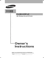
PLASMA DISPLAY PANEL

SPECIFICATIONS AND PARTS ARE SUBJECT TO CHANGE FOR IMPROVEMENT

R/C: 

CLU-4352UG2  

55

HDS69

N T S C

DW 2-U

Chassis

SERVICE MANUAL

SERVICE MANUAL REVISION HISTORY INFORMATION

DATE        REVISON #

 REASON

May , 06     SM00001         FIRST ISSUE OF MANUAL 

R/C: CLU-3861WL   

55HDT79/55HDX99

A

T S C

MAY 2006


HHEA


MANUFACTURIN

G DIVISION

Added part number for interconnect cable

CH 4

Summary of Contents for 42HDT79 - UltraVision CineForm - 42" Plasma TV

Page 1: ... TO CHANGE FOR IMPROVEMENT R C CLU 4352UG2 55HDS69 N T S C DW 2 U Chassis SERVICE MANUAL SERVICE MANUAL REVISION HISTORY INFORMATION DATE REVISON REASON May 06 SM00001 FIRST ISSUE OF MANUAL R C CLU 3861WL 55HDT79 55HDX99 A T S C MAY 2006 HHEA MANUFACTURING DIVISION Added part number for interconnect cable CH 4 ...

Page 2: ...by qualified service personnel only To reduce the risk of electric shock do not perform any servicing other than that contained in the operating instructions unless you are qualified to do so Before servicing this chassis it is important that the service technician read the IMPORTANT SAFETY INSTRUCTIONS in this service manual SAFETY NOTICE USE ISOLATION TRANSFORMER WHEN SERVICING Components having...

Page 3: ... Line 1 and Line 2 of the three plug prongs do not connect with the third prong which is physical ground Using an insulation tester DC500V connect one of its leads to the AC plug jumper and touch with the other lead each exposed metal part antennas screwheads metal overlays control shafts etc particularly any exposed metal part having a return path to the chassis should have a resistor reading ove...

Page 4: ...e take special care with this fragile circuitry particularly Flexible Printed Circuits bonded to surrounding edges of the glass panel They are not strong enough to withstand harsh outer mechanical forces Avoid touching the flexible printed circuits by not only your hands but also tools chassis or any other object Extreme bending of the connectors must be avoided too In case the flexible printed ci...

Page 5: ...statically Sensitive ES Devices Some semiconductor solid state devices can be damaged easily by static electricity Such components commonly are called Electrostatically Sensitive ES Devices Examples of typical ES devices are integrated circuits and some field effect transistors and semiconductor chip components The following techniques should be used to help reduce the incidence of component damag...

Page 6: ...lly insert the replacement IC in the circuit board 2 Carefully bend each IC lead against the circuit foil pad and solder it 3 Clean the soldered areas with a small wire bristle brush It is not necessary to reapply acrylic coating to areas Small signal Discrete Transistor Removal Replacement 1 Remove the defective transistor by clipping its leads as close as possible to the component body 2 Bend in...

Page 7: ...ue only on IC connections 1 Carefully remove the damaged copper pattern with a sharp knife Remove only as much copper as absolutely necessary 2 Carefully scratch away the solder resist and acrylic coating if used from the end of the remaining copper pattern 3 Bend a small U in one end of a small gauge jumper wire and carefully crimp it around the IC pin Solder the IC connection 4 Route the jumper ...

Page 8: ... soldering pads with tweezers or with a miniature alligator clip and apply heat to the pad area with a 30 watt iron until solder flows Do not apply heat for more than 3 seconds How to Replace Flat lC Required Tools Soldering iron iron wire or small awl De solder braids Magnifier 1 Remove the solder from all of the pins of a Flat lC by using a de solder braid 2 Put the iron wire under the pins of t...

Page 9: ...move previous solder as much as possible from the soldering point When soldering please perfectly melt the lead free solder to mix well with the previous solder 3 Soldering iron for lead free solder Melting point of lead free solder is higher than solder containing lead Use of a soldering tool with temperature control and with much thermal capacitance is recommended Recommended temperature control...

Page 10: ... cause harmful interference to radio communications However there is no guarantee that interference will not occur in a particular installation If this equipment does cause harmful interference to radio or television reception which can be determined by turning the equipment off and on the user is encouraged to try to correct the interference by one or more of the following measures Reorient or re...

Page 11: ...ESA is a trademark of a nonprofit organization Video Electronics Standard Association This Class B digital apparatus meets all requirements of the Canadian Interference Causing Equipment Regulations This Class B digital apparatus complies with Canadian ICES 003 Cet appareil numérique de la classe B est conforme à la norme NMB 003 du Canada Cable Compatible Television Apparatus Tèlèvision câblocomp...

Page 12: ...nel The 42 and 55 TV s contain the displaying device which is the plasma display panel module and the driving circuitry which receives the signal from the Digital AV Block and after processing delivers the image to the display module This HITACHI Service Manual is intended for the qualified service personnel and it contains the necessary information for troubleshooting the Plasma television set in...

Page 13: ...Contrast Mode Color Management Decoding Auto Color Noise Reductfon Auto Movie Mode Black Side Panel 24 Vol Balance Bass Treble Source Internal Speakers 25 Adjustment Settings for Sound 26 Auto Noise Cancel Perfect Volume Mute Soft Mute PinP Split 27 With ANT CABLE DIGITAL CHANNEL Video 480i 720p 1080i Mode Strobe 28 With 3Pix only ANT CABLE DIGITAL CHANNEL Video 480i Except Photo Input only HDT HD...

Page 14: ... 3 lnput HDMI 18P X3 Selected by component Video1 2 5 Digital input priority Audio In L R Lch mono 54 5 lnput RCApinx10 Auto Link 55 1 Input VIDEO2 LINK Auto Link Function Video Control Terminal BS 56 No U V Ant Input 57 CABLE AIR BS I F Input 58 No Video Monitor Out Terminal 59 1 Output RCA pin x 1 Audio Output Terminal 60 1 Output UR RCA pin x 2 Common input for No 59 Audio Monitor Out Terminal ...

Page 15: ...r Ext SPLIT X Rotate PANA Black X X X AC3 Downmix Digital Tuner Ext SPLIT Rotate PANA Black X X AC3 Downmix Digital Tuner Ext SPLIT TVU Hoshiden BLACK X AC3 Downmix Remote Sound function Model Name Class 55HDX99 HDX 55HDT79 HDT 55HDS69 HDS TV Output Speaker RS232C IR Out YPbPr S IN AV IN S V AUDIO Y As 6CH RF Center Watt IEEE1394 HDMI Ver1 1 OUT OUT OUPUT Composite OUT L mono 36 2FR2W 1 2 1 2 2 1H...

Page 16: ...ch PUSH LOCK 1 switch Panel Operation Power Switch PUSH NON LOCK 1 switch Input Terminal Video Audio Input RCA HDMI DV connector Audio Line Output Sub Woofer Output 1 system Output Terminal Speaker Output Connector 3 Polarity Receptacle Power Supply Source Input Voltage Single Phase AC108 132V 6 OHz Temp Operating 5 35 C 41F 95F Temperature Stored 15 60 C 5F 140F Humidity Operating 20 80 RH Non co...

Page 17: ... Yes Yes Yes Yes Input 3 YPBPR 1080i 720p 웎 16x9 Yes Yes Yes 웎 Yes 웎 웎 480p Auto ON 16x9 Yes Initial 웎 Yes 웎 웎 웎 웎 480i Letter 웎 웎 웎 Yes Yes Yes Initial Yes 4x3 웎 웎 웎 Yes Yes Initial Yes Yes No ID Yes 웎 Yes Yes Yes Yes Yes Auto OFF 웎 No Signal 웎 웎 Video NTSC Auto ON 16x9 Yes Initial 웎 Yes 웎 웎 웎 웎 Letter 웎 웎 웎 Yes Yes Yes Initial Yes 4x3 웎 웎 웎 Yes Yes Initial Yes Yes No ID Yes 웎 Yes Yes Yes Yes Yes...

Page 18: ...x3 4 3 Standard 16 9 Standard2 16x9 90 16x9 4 3 Expanded 75 75 16 9 Zoom 4x3 75 56 4x3 4 3 Zoom2 75 4 3 Zoom1 4x3 90 4x3 4 3 Expanded 75 75 16x9 16 9 Zoom 162 113 4 3 Expanded Mode Horizontal Expansion Ratio Horizontal Position 100 4x3 Format 100 16x9 Format 4 3 Expanded 162 113 162 17 DW2U ...

Page 19: ... Aspect 4x3 Aspect Key Aspect Key Aspect Key Aspect Key 4 3 Standard 4 3 Zoom2 4 3 Expanded 4 3 Zoom1 3 HDMI YPBPR 1080i 720p 4 HDMI YPBPR 480p 480i Video S Video 4 1 Auto Aspect OFF 4 2 Auto Aspect ON a Video ID HDMI Info 16x9 4 3 Zoom1 16 9 Zoom 4 3 Expanded 16 9 Standard1 4 3 Zoom2 4 3 Standard Aspect Key Aspect Key Aspect Key Aspect Key Aspect Key Aspect Key Video ID 16x9 Power ON Initial Aspe...

Page 20: ...50 lines Input 1 2 HDMI 1080i 720p 16x9 0 step Gray out 10 step 30 lines 웎 10 step 10 lines 웎 웎 480p 480i 16x9 4x3 0 step Gray out 10 step 30 lines 0 step Gray out 10 step 10 lines 10 step 30 lines 10 step 50 lines S Video Video NTSC 웎 0 step Gray out 10 step 30 lines 0 step Gray out 10 step 10 lines 10 step 30 lines 10 step 50 lines Input 3 4 YPBPR 1080i 720p 16x9 0 step Gray out 10 step 30 lines...

Page 21: ... 웎 웎 웎 웎 웎 웎 웎 웎 웎 웎 웎 웎 1080i 16x9 웎 웎 웎 Yes 웎 Yes 웎 웎 웎 웎 웎 웎 720p 16x9 웎 웎 웎 Yes 웎 Yes 웎 웎 웎 웎 웎 웎 480p 16x9 웎 웎 웎 Yes 2 웎 Yes 2 웎 웎 웎 웎 웎 웎 480p 4x3 웎 웎 웎 웎 웎 웎 웎 웎 웎 웎 웎 웎 480i 16x9 웎 웎 웎 Yes 2 웎 Yes 2 웎 웎 웎 웎 웎 웎 PIP 4x3 Component Composite S IN HDMI 480i 4x3 웎 웎 웎 웎 웎 웎 웎 웎 웎 웎 웎 웎 1080i 16x9 웎 웎 웎 웎 웎 웎 Yes Yes Yes Yes Yes Yes 720p 16x9 웎 웎 웎 웎 웎 웎 Yes Yes Yes Yes Yes Yes 480p 16x9 웎 웎 웎 웎...

Page 22: ...RF Mode is not displayed at a V Chip setup SPLIT Mode is displayed at this time When EXIT Key is pushed PIP turns off When PIP is turns off PIP Mode of a display turns into Last Mode 2 Freeze Operation Exit Key Freeze Key Freeze Key Freeze Key Freeze Key STROBE Sub Frozen Main Moving Main Frozen 3 SWAP Operation Key B A B PIP OFF PIP OFF A A A B B B A B A Key Key Main Audio Sub Audio Sub Audio Mai...

Page 23: ...웎 YES S Video_1 YES YES YES YES Video_1 웎 YES YES YES Input2 HDMI_2 웎 웎 웎 YES S Video_2 YES YES YES YES Video_2 웎 YES YES YES Input3 YPBPR_3 웎 웎 웎 YES Video_3 웎 YES YES YES Input4 YPBPR_4 웎 웎 웎 YES Video_4 웎 YES YES YES Input5 HDMI_5 웎 웎 웎 YES Side YPBPR_5 웎 웎 웎 YES Video_5 웎 YES YES YES 4 2 Set the Monitor out TV out Monitor Out D B A B A B A B A Monitor Out C B A B A Key Key Key Main Audio Sub A...

Page 24: ...T YES ANT YES ANT YES ANT CABLE Digital Channel Macrovision S Video 웎 웎 웎 YES ANT Analog Channel Video 웎 YES ANT YES ANT YES ANT Input_1 HDMI_1 YPBPR S Video_1 Video_1 Input_2 HDMI_2 YPBPR S Video_2 Video_2 Input_3 YPBPR_3 Video_3 Input_4 YPBPR_4 Video_4 Input_5 HDMI_5 YPBPR Side YPBPR_5 Video_5 YES ANT Digital only YES ANT YES ANT YES ANT When Macrovision signal is included in the ANT Digital cha...

Page 25: ...r color TV antenna is recommended for best performance However if you are located in an exceptionally good signal area that is free from interference and multiple image ghosts an indoor antenna may be sufficient LOCATION Select an area where sunlight or bright indoor illumination will not fall directly on the picture screen Also be sure that the location selected allows a free flow of air to and f...

Page 26: ...ement for best performance ANTENNA CONNECTIONS TO REAR JACK PANEL VHF 75 Ohm antenna CATV Cable TV When using a 75 Ohm coaxial cable system connect CATV coaxial cable to the AIR CABLE 75 Ohm terminal Or if you have an antenna connect the coaxial cable to the same AIR CABLE terminal VHF 300 Ohm antenna UHF antenna When using a 300 Ohm twin lead from an outdoor antenna connect the VHF or UHF antenna...

Page 27: ... connect to inputs and outputs located on the rear jack panel and front control panel USB Cable HDT HDX only This cable is used to connect your digital camera to the Photo Input in the side of the Plasma television IR Mouse Cable Provided HDT HDX only Connect the IR Mouse to the IR output of your Plasma Television when A V Network is used You must place the IR mouse in front of the corresponding I...

Page 28: ...TONS TV DVD CBL STB PVR VCR AMP CD Used to manually enter the TV channel and used for numeric entry when navigating through the OSD INPUTS and AV NET menu systems GUIDE BUTTON TV STB CBL PVR Accesses the TV Guide On Screen system see page 54 of the TV or the program guide of other devices EXIT BUTTON TV CBL STB PVR VCR Exits out of the OSD INPUTS or AV NET menu systems if their menu is displayed L...

Page 29: ...ge the Picture in Picture mode EXIT BUTTON TV CBL SAT Exits out of the OSD or INPUTS menu systems if their menu is displayed FAVORITE CHANNEL FAV CH button TV Press to enter access Favorite Channel FAV mode GUIDE BUTTON SAT CBL Accesses the program guide of other devices INFO BUTTON TV CBL SAT Displays various information on the screen CHANNEL BUTTONS TV CBL SAT VCR Changes the channel LAST CHANNE...

Page 30: ...EXIT button Press this button to access the INPUT menu Press again to exit the MENU mode 햶 CHANNEL selector Press these buttons until the desired channel appears in the top right corner of the TV screen These buttons also serve as the cursor down and up buttons when in MENU mode 햷 VOLUME level Press these buttons to adjust the sound level The volume level will be displayed on the TV screen These b...

Page 31: ...f Lights Red Off OFF Lights Blue Off Off Turning ON OFF TV MAIN POWER is ON but no picture is shown TV MAIN POWER is ON picture is shown Lights Orange Off Off NOTES 1 Your HITACHI Plasma TV will appear to be turned OFF lights orange if there is no video input when INPUT 1 2 3 4 and 5 Check the Power Light to make sure the TV is turned off or in Stand by mode lights red when not in use 2 Remote Con...

Page 32: ...ion DTV signals remain in digital format HDMI assures that pristine high definition images retain the highest video quality from the source all the way to your television screen Use the HDMI input for your external devices such as Set Top Boxes or DVD players equipped with an HDMI output connection HDMI the HDMI logo and High Definition Multimedia Interface are trademarks or registered trademarks ...

Page 33: ... 19 When using IEEE1394 connections you enable video and audio digital data exchange between a compatible device This connection also enables you to control basic equipment functions such as VCR play rewind fast forward stop etc from your TV On Screen Display Only HDT HDX models Digital Cable INSERT INSERT NOTE 1 A digital cable subscription is required 2 Do not insert a PCMCIA card into the Cable...

Page 34: ...rd plugs when connecting to left side panel jacks If you do not the played back picture may be abnormal l e n a P e d i S t f e L R AUDIO L MONO Y VIDEO INPUT 5 specifications Note Special device cables will be according to the own device Video Game OUTPUT PB C B PR CR R L PR PB Y Video Camera COMPONENT OUTPUT CAPABILITY DVD Set Top Box Video Game Console l e n a P e d i S t f e L R AUDIO L MONO Y...

Page 35: ...rticular assortment of components and features For best performance video and audio cables should be made from coaxial shielded wire Before Operating External Video Source Connect an external source to one of the INPUT terminals then press the INPUTS button to show the INPUTS menu Use the CURSOR PAD and to select the Antenna or Input of your choice Then press the SELECT button or the CURSOR PAD to...

Page 36: ...itter Outside Antenna ANT IN OUTPUT S VIDEOV L R DIGITAL OUTPUT CAPABILITY DIGITAL OUTPUT Laserdisc player VCR camcorder etc OUTPUT Y P B PR L R HDTV Set Top Box DVD Player DVI to HDMI AUDIO OUT OUTPUT Y PB CB PR CR L R VCR 2 V L R OUTPUT S VIDEO V L R INPUT S VIDEO Optional Optional HDMI DIGITAL OUTPUT CAPABILITY HDMI OUTPUT HDMI to HDMI DVHS DV or 1394 OUTPUT CAPABILITY DV or 1394 OUTPUT ...

Page 37: ... in place of the standard video connection if your device has this feature Your component outputs may be labeled Y B Y and R Y In this case connect the components B Y output to the TV s PB input and the components R Y output to the TV s PR input Your component outputs may be labeled Y CBCR In this case connect the components CB output to the TV s PB input and the components CR output to the TV s P...

Page 38: ...ination the brightness of the phosphor will be degraded to such extent that stationary images would burn in that part of the screen as grayed out images Tips to prevent such image retention are Do not display images having sharp brightness differences or hi contrast images such as monochrome characters and graphic patterns for long Do not leave stationary images appearing for long but try to refre...

Page 39: ...ightness Check 40 4 POWER SUPPLY Vs Va Voltage Adjustment 41 5 White balance adjustment 42 5 1 Video Color Temperature Adjustment High 42 5 2 Video Color Temperature Adjustment Medium 42 5 3 Video Color Temperature Adjustment Standard 43 5 4 Video Color Temperature Adjustment Black and White 43 5 5 White Balance Adjustment OSD Flowchart Diagram 44 6 DIGITAL MAIN CHECK 43 7 Screen Check 46 8 HDMI A...

Page 40: ...Use any Hitachi remote control when making an adjustment keys are used for selecting adjustment item keys are used for changing data values MENU key is used to advance through the adjustment mode menus and pages Remote Control Buttons Change Selection Up Increase Data Value Change Selection Down Increase Data Value ADJUST MODE FACT RESET MEMORY INIT RGB WHITE BAL HIGH WHITE BAL MED WHITE BAL STD W...

Page 41: ... operation is complete and do not perform any key operation either after this operation each factory setting and all adjust mode data should reset to delivery settings automatically 7 After Memory Initialize it should be unplug AC cord Unplug and plug AC cord and then all settings and data are updated The adjustment item that is affected by the memory initialize operation is shown below Note Perfo...

Page 42: ...ithin r0 2V of the value specified in the label on the panel Va withinr0 2V 42 Adjusted by manufacturing 55 Need to be adjusted 3 Connect voltmeter which has an error within 0 02V or less leads to Vs or Va and GND test points of the power unit 3 Reconfirm that Vs voltage remains within r0 1V of the specified value Readjust if it s outside of the margin Label example Label position Reference Upper ...

Page 43: ...east one of the data should be FF Specification Video Color temperature HIGH x 0 273 42 0 005 y 0 273 0 005 Color temp 12000K x 0 273 55 0 005 y 0 273 0 005 Color temp 12000K Remarks 1 Color temperature should be adjusted under the condition in which the screen is the brightest thus the initial value for adjustment is set to its maximum 2 Adjustment is made by reducing brightness only Reduce a bri...

Page 44: ...0K Specification Video Color temperature B W x 0 335 42 0 005 y 0 343 0 005 Color temp 5400K x 0 335 55 0 005 y 0 343 0 005 Color temp 5400K 6 DIGITAL MAIN CHECK 6 1 SYSTEM SOFTWARE VERSION CHECK Please Insert MMC card ove Return 5 The upgrading process begin by filling a bar when finish the message will say Upgrade complete when this appear unplug the TV from the AC line outlet to complete the pr...

Page 45: ... WHITE BAL HIGH WHITE BAL MED WHITE BAL STD WHITE BAL B W CH U D INPUT ًٕ ًٕ ًٕ CYAN GREEN Finish Normally RED Finish Abnormally EXIT Press for 2 seg ADJUST MODE MEMORY INIT FACT RESET RGB WHITE BAL HIGH WHITE BAL MED WHITE BAL STD WHITE BAL B W CH U D INPUT ADJUST MODE MEMORY INIT FACT RESET RGB WHITE BAL HIGH WHITE BAL MED WHITE BAL STD WHITE BAL B W CH U D INPUT MAGENTA GREEN Finish Normally RE...

Page 46: ...to adjust ًٕ 45 DW2U BACK TO ADJUSTMENTS 5 7 1 Adjustment OSD Flowchart Cont ًٕ G DRV R DRV B DRV ًٕ G DRV HIGH R DRV HIGH B DRV HIGH Select DRV and Press key Press EXIT key ADJUST MODE MEMORY INIT FACT RESET RGB WHITE BAL HIGH WHITE BAL MED WHITE BAL STD WHITE BAL B W CH U D INPUT ADJUST MODE MEMORY INIT FACT RESET RGB WHITE BAL HIGH WHITE BAL MED WHITE BAL STD WHITE BAL B W CH U D INPUT ...

Page 47: ...color bar and small multi burst Confirm that the picture appears as shown below or similar 2 Press INFO button on remote control to confirm that 1080i Format indication appears 3 Confirm that Horizontal and Vertical position meet the following spec BACK TO ADJUSTMENTS 9 FACTORY RESET After all of the adjustments of main chassis are finished perform FACTORY RESET 1 Enter Adjustment Mode by the meth...

Page 48: ...T79 55HDT79 42HDX99 55HDX99 Input Mode Air X X X Channel 03 1ch X X X Favorite Channels Not Registered X X X PIP On Off Off X X X PIP Mode SPLIT X X X POP Position Middle Right X X X PIP Position Bottom Right X X X Freeze Mode Main Freeze 1pix X X X Master Volume 20 Step X X X Video Picture Mode Dynamic X X X Contrast White Lebel 100 X X X Brightness Black Lebel 50 X X X Color 50 X X X Tint CENTER...

Page 49: ... X X X Reset 웎 X X X Start 웎 X X X Channel List FAV Not Set X X X CH Air Cable 2 13CH X X X Scan On X X X Lock Off X X X ID 웎 X X X Locks Change Access Code 0000 7777 X X X Engage Lock Set Channel Lock Not Set X X X Set Front Panel Lock Not Set X X X Movie Ratings Not Set X X X TV Ratings Not Set X X X Canadian Ratings Eng Not Set X X X Canadian Ratings Frn Not Set X X X Alternate Ratings U S X X ...

Page 50: ...Input4 Auto Link Auto Remote Off Off X X X Input5 Rename None X X X Set the AV Net Wizard will be starting X 웎 웎 Set Closed Caption Caption Display Auto X X X Mode Captions Text Captions X X X Channel 1 2 3 4 1 X X X Digital Captions Language 1 English X X X Font Default 1 2 3 4 5 6 7 8 Default X X X Size Small Standard Large Standard X X X Style Standard High Visibility Standard X X X Set The Out...

Page 51: ... button to set 4 Unpluged and pluged to update the OSD Design Adjustment Procedure 1 According to a list shown below select an OSD design Class Model DATA OSD Design X 42 55HDX99 5 웛 LUHFWRUV T 42 55HDT79 웛5HJLRQDO S 42 55HDS69 웛1DWLRQDO DATA 2웛DIREC웉Directors Model웊 DATA 1웛A웉Regional Model웊 DATA 0웛B웉National Model웊 ADJUST MODE IR BLAST CLOCK TEST MAINTENANCE DEVICE M306H3 V01 00 ADJ REV V01 00 PA...

Page 52: ...is turn off the LED is Lighting the LED After Program is loaded without error all LED will be turned off Any LED should not light If some errors occur LED will show the error pattern 1 Check that LED is not lit 2 If LED is lit refer to the following table and check the involved devices TROUBLE SHOOTING for DIGITAL MODULE Device error check TABLE OF CONTENTS TROUBLESHOOTING FLOW CHARTS Location of ...

Page 53: ...Cable Air 4 ٤ ٤ ٨ ٤ ٤ MPEG Seine2 Video Audio of Cable Air 5 ٤ ٤ ٨ ٤ ٨ Graphics Seine2 All OSD 6 ٤ ٤ ٨ ٨ ٤ Flash Memory Loading Program 7 ٤ ٤ ٨ ٨ ٨ I 2 C Seine2 8 ٤ ٨ ٤ ٤ ٤ IEEE1394 9 ٤ ٤ ٤ ٨ ٨ DEMUX Seine2 10 ٤ ٨ ٤ ٨ ٤ 㧙 㧙 11 ٤ ٨ ٤ ٨ ٨ 㧙 㧙 12 ٤ ٨ ٨ ٤ ٤ 㧙 㧙 13 ٤ ٨ ٨ ٤ ٨ 㧙 㧙 14 ٤ ٨ ٨ ٨ ٤ 㧙 㧙 15 ٤ ٨ ٨ ٨ ٨ 㧙 㧙 16 ٨ ٤ ٤ ٤ ٤ 㧙 㧙 17 ٨ ٤ ٤ ٤ ٨ PDP Panel 18 ٨ ٤ ٤ ٨ ٤ Sub Micro 19 ٨ ٤ ٨ ٤ ٨ Seine OSD 20 ٨ ...

Page 54: ...te Control LED PWB IR Receiver LED POD Card I F Side Terminal PWB A V Control PWB Key SW RGB LVDS CPUgo PDPgo Power2 Power1 Sub PWB OPT Audio Output A V SD MMC Card I F RS 232C Filter PWB Main Power SW AC Inlet Demodulator Video SW Digital Analog Tuner A V Pin Jack Audio SW Power Supply Unit Main Digital PWB Sub Micro Audio DSP Seine2 A chip Seine2 D chip HDMI PWB Equalizer DC DC POD Vcc PLD Obero...

Page 55: ...V Control PWB Key SW RGB LVDS Photo CPUgo PDPgo Power2 Power1 Sub PWB IR Out OPT Audio Output A V SD MMC Card I F RS 232C Filter PWB Main Power SW AC Inlet Demodulator Video SW Digital Analog Tuner A V Pin Jack Audio SW Motor Driver Power Supply Unit Main Digital PWB Sub Micro Audio DSP Seine2 A chip Seine2 D chip HDMI PWB Equalizer DC DC POD Vcc PLD Oberon VCXO PLL PLD Stehano DC DC Conv Audio DA...

Page 56: ...B LVDS Photo CPUgo PDPgo Power2 Power1 Sub PWB IR Blaster Driver OPT Audio Output A V SD MMC Card I F RS 232C Filter PWB Main Power SW AC Inlet Demodulator Video SW Digital Analog Tuner A V Pin Jack Audio SW UEI Motor Driver Power Supply Unit Main Digital PWB Sub Micro Audio DSP Seine2 A chip Seine2 D chip HDMI PWB Equalizer DC DC POD Vcc PLD Oberon VCXO PLL IEEE 1394 PLD Stehano DC DC Conv Audio ...

Page 57: ... IR Blaster Driver 5V Reg OPT Output 9V Reg LPF 5V Reg Sync sep 5V Reg USB FAN Vari Reg 1 0V DC DC 1 8V Reg Demodulator 3 3V Reg 2 5V Reg 1 5V Reg 3 3V Reg Seine2 A 2 5V Reg Audio DSP HDMI PWB 3 3V Reg Cable Equalizer 9V Reg AV SW 5V Reg 5V Reg Tuner AGC OOB 3 3V Reg Audio ADC 3 3V Reg Audio DAC 9V Reg FAN 1 8V DC DC 1 3V DC DC 2 5V Reg Seine2 D DDR2 1 3V Reg 1 5V Reg IEEE1394 Vari Reg POD Vpp 3 3...

Page 58: ...F12 TPA3100 Digital Power Amp IF15 NJU26107 Volume Mute Balance Bass Treble Surround Bass Boost AGC IF11 TPA3100 Digital Power Amp I2S I2S IF09 WM8520 DAC W amp I2S IF10 WM8520 DAC W amp IF20 SN74LV C244AP W Woofer L Woofer R Speaker L Speaker R ...

Page 59: ...㪇 㪈㪍㪈 㪤㪧㪜㪞㪶㪧㪪㪰㪥㪚 㪛㪜㪪㪫㪇 㪈㪍㪉 㪈㪍㪊 㪤㪧㪜㪞㪶㪧㪜㪥 㪛㪜㪪㪫㪈 㪈㪍㪋 㪈㪍㪌 㪞㪥㪛 㪞㪥㪛 㪈㪍㪍 㪈㪍㪎 㪪㪫㪭㪶㪘㪝㪚 㪘㪭㪚㪫㪯㪛 㪈㪍㪏 㪈㪍㪐 㪤㪫㪭㪶㪘㪝㪚 㪘㪭㪚㪩㪯㪛 㪈㪎㪇 㪈㪎㪈 㪘㪭㪚㪚㪫㪪㪶㪥 㪈㪎㪉 㪈㪎㪊 㪘㪭㪚㪩㪫㪪㪶㪥 㪈㪎㪋 㪈㪎㪌 㪚㪈㪶㫀㪥 㪞㪥㪛 㪈㪎㪍 㪈㪎㪎 㪪㫀㪞㪶㪛㪜㪫 㪚㪩㪯㫀㪥 㪈㪎㪏 㪈㪎㪐 㪛㪩㪯㫀㪥 㪈㪏㪇 㪈㪏㪈 㪫㪭㪪㪶㪣 㪪㪮㪶㪪㪜㪣 㪈㪏㪉 㪈㪏㪊 㪞㪥㪛 㪛㫀㪧㪶㪛㪜㪫 㪈㪏㪋 㪈㪏㪌 㪫㪯㪛㪂 㪉㪊㪉㪚㪶㪪㪜㪣 㪈㪏㪍 㪈㪏㪎 㪞㪥㪛 㪜㪯㪫㪶㪩㪜㪪㪜㪫 㪈㪏㪏 㪈㪏㪐 㪫㪯㪛㪄 㪛㪫㪫㪶㪧㫆㪮㪜㪩 㪈㪐㪇 㪈㪐㪈 㪞㪥㪛 㪞㪥㪛 㪈㪐㪉 㪈㪐㪊 㪩㪯㫀㪥㪂 㪈㪐㪋 㪈㪐㪌 㪞㪥㪛 㪈㪐㪍 㪈㪐㪎 㪩㪯㫀㪥㪄 㪈㪐㪏 㪈㪐㪐 㪞㪥㪛 㪞㪥㪛 㪉㪇㪇 㪛㪂㪊㪅㪊㪭 㪏㪇 㪈 㪛㪂㪊㪅㪊㪭 㪪...

Page 60: ...㪶㪪 㪌㪍 㪧㪥㪣㫆㪥 㪊㪍 㪈 㪭㪚㪚 㪌㪎 㪪㪜㪣㪶㪩㪶㪪 㪞㪥㪛 㪌㪏 㪫㪜㪤㪧㪶㪘㪣㪫 㪊㪎 㪉 㪣㫆㪚㪢 㪌㪐 㪞㪥㪛 㪟㫀㪝㫀㪶㪩 㪍㪇 㪛㫆㫆㪩㪶㪘㪣㪫 㪊㪏 㪊 㪞㪥㪛 㪍㪈 㪪㪚㪣㪈㪶㪊㪭㪶㪈㪇㪇 㪟㫀㪝㫀㪶㪣 㪍㪉 㪠㪩㪨㪆㪝㪘㪥㪶㪘㪣㪫 㪊㪐 㪍㪊 㪪㪛㪘㪈㪶㪊㪭㪶㪈㪇㪇 㪞㪥㪛 㪍㪋 㪧㪛㪮㪥 㪋㪇 㪍㪌 㪞㪥㪛 㪟㪛㪛㪶㪣 㪍㪍 㪙㪣㪶㪧㪮㪤 㪋㪈 㪍㪎 㪍㪌㪍㪶㪛㪐 㪟㪛㪛㪶㪩 㪍㪏 㪍㪐 㪍㪌㪍㪶㪛㪏 㪞㪥㪛 㪎㪇 㪎㪈 㪍㪌㪍㪶㪛㪎 㪪㪜㪣㪶㪣㪶㪤 㪎㪉 㪎㪊 㪍㪌㪍㪶㪛㪍 㪪㪜㪣㪶㪩㪶㪤 㪎㪋 㪎㪌 㪍㪌㪍㪶㪛㪌 㪞㪥㪛 㪎㪍 㪎㪎 㪍㪌㪍㪶㪛㪋 㪬㪘㪫㪯㪛㪊 㪎㪏 㪎㪐 㪍㪌㪍㪶㪛㪊 㪬㪘㪩㪯㪛㪊 㪏㪇 㪏㪈 㪍㪌㪍㪶㪛㪉 㪞㪥㪛 㪏㪉 㪏㪊 㪍㪌㪍㪶㪛㪈 㪬㪘㪩㪫㪪㪊㪶㪥 㪏㪋 㪏㪌 㪍㪌㪍㪶㪛㪇 㪬㪘㪚㪫㪪㪊㪶㪥 㪏㪍 㪏㪎 㪞㪥㪛 㪤㪛㪤㪶㪛㪚㪛㪶...

Page 61: ...㪪㪛㪛㪘㪫㪉 㪪㪛㪛㪘㪫㪈 㪈㪋 㪍㪎 㪪㪛㪛㪘㪫㪈 㪪㪛㪮㪧 㪈㪊 㪍㪏 㪪㪛㪮㪧 㪪㪛㪛㪘㪫㪇 㪈㪉 㪍㪐 㪪㪛㪛㪘㪫㪇 㪪㪛㪚㪛 㪈㪈 㪎㪇 㪪㪛㪚㪛 㪪㪛㪚㪤㪛 㪈㪇 㪎㪈 㪪㪛㪚㪤㪛 㪞㪥㪛 㪐 㪎㪉 㪞㪥㪛 㪪㪛㪚㪣㪢 㪏 㪎㪊 㪪㪛㪚㪣㪢 㪞㪥㪛 㪎 㪎㪋 㪞㪥㪛 㪍 㪎㪌 㪂㪌㪅㪍㪭 㪌 㪎㪍 㪂㪌㪅㪍㪭 㪂㪌㪅㪍㪭 㪋 㪎㪎 㪂㪌㪅㪍㪭 㪂㪌㪅㪍㪭 㪊 㪎㪏 㪂㪌㪅㪍㪭 㪂㪌㪅㪍㪭 㪉 㪎㪐 㪂㪌㪅㪍㪭 㪂㪌㪅㪍㪭 㪈 㪏㪇 㪂㪌㪅㪍㪭 㪮㪧 㪉㪈 㪈 㪮㪧 㪟㪧㪛 㪉㪇 㪉 㪟㪧㪛 㪂㪌㪭㪛㪜㪫 㪈㪐 㪊 㪂㪌㪭㪛㪜㪫 㪞㪥㪛 㪈㪏 㪋 㪞㪥㪛 㪪㪛㪘 㪈㪎 㪌 㪪㪛㪘 㪪㪚㪣 㪈㪍 㪍 㪪㪚㪣 㪘㪚㪢 㪈㪌 㪎 㪘㪚㪢 㪪㪰㪥㪚㪂㪌㪭 㪈㪋 㪏 㪪㪰㪥㪚㪂㪌㪭 㪞㪥㪛 㪈㪊 㪐 㪞㪥㪛 㪩㪯㪚㪄 㪈㪉 㪈㪇 㪩㪯㪚㪄 㪩㪯㪚㪂 㪈㪈 㪈㪈 㪩㪯㪚㪂 㪞㪥㪛 㪈㪇 㪈㪉...

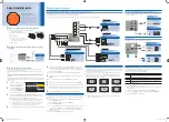
Page 62: ...DW2U 59 FINAL WIRING DIAGRAM TABLE OF CONTENTS ...

Page 63: ...QUICK DISASSEMBLE GUIDE Back Cover 1 TABLE OF CONTENTS 60 DW2U Remove Screw M3M 6 18HX 2 Pcs Remove Screw M3M 6 18HX 2 Pcs Remove Screw M3M 6 12X 2 Pcs ...

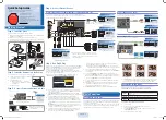
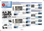
Page 64: ...QUICK DISASSEMBLE GUIDE Back Cover 2 61 DW2U BACK COVER Remove Screw M3D_4 10BD 34 Pcs ...

Page 65: ...QUICK DISASSEMBLE GUIDE Power Unit 62 DW2U POWER UNIT Remove Screw M3E 3 8 3 Pcs Remove Screw M3M 3 8 3 Pcs ...

Page 66: ...QUICK DISASSEMBLE GUIDE Chassis Block 63 DW2U Remove Screw M3E 4 10 2 Pcs CHASSIS BLOCK ...

Page 67: ...K DISASSEMBLE GUIDE Terminal Metal 64 DW2U Remove Screw M3E 3 8 4 Pcs Remove Screw D Su51 2 Pcs Remove Tuner Nut and Washer Remove Screw T2B 3 10 4 Pcs Remove Screw M3E 3 8 4 Pcs Remove Screw M3M 3 6 4 Pcs ...

Page 68: ...QUICK DISASSEMBLE GUIDE POD PWB 65 DW2U Remove Screw M3E 3 8 Remove POD PWB Assy ...

Page 69: ...QUICK DISASSEMBLE GUIDE Main Sub Digital PWB 66 DW2U Remove Main Digital PWB Assy Remove Sub Digital PWB Assy IS NECESSARY TO RELEASE MAIN PWB AND SUB PWB FROM BOARD HOLDERS 3 POSITIONS ...

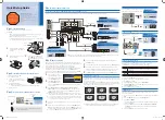
Page 70: ...FINAL ASSEMBLY GUIDE TABLE OF CONTENTS 67 DW2U ...

Page 71: ...FINAL ASSEMBLY GUIDE 68 DW2U ...

Page 72: ...FINAL ASSEMBLY GUIDE 69 DW2U ...

Page 73: ...FINAL ASSEMBLY GUIDE 70 DW2U ...

Page 74: ...FINAL ASSEMBLY GUIDE 71 DW2U ...

Page 75: ...FINAL ASSEMBLY GUIDE 72 DW2U ...

Page 76: ...FINAL ASSEMBLY GUIDE 73 DW2U ...

Page 77: ...FINAL ASSEMBLY GUIDE 74 DW2U ...

Page 78: ...FINAL ASSEMBLY GUIDE 75 DW2U ...

Page 79: ...FINAL ASSEMBLY GUIDE 76 DW2U ...

Page 80: ...ync 60 hz and a X10 probe Numbers inside circle correspond to locations shown in the circuit diagram Waveforms taken WAVEFORMS Signal amplitude and DC level shown at and respectively DW2U 4 0 V 4 0 V 4 0 V 4 0 V 4 0 V 4 0 V 4 0 V 4 0 V IT02 Pin 42 MPEG DATA 1 IT02 Pin 47 MPEG DATA 2 IT02 Pin 48 MPEG DATA 3 IT02 Pin 50 MPEG DATA 4 IT02 Pin 51 MPEG CLK 8 9 5 IT02 Pin 54 MPEG DATA 5 IT02 Pin 57 MPEG ...

Page 81: ...ync 60 hz and a X10 probe Numbers inside circle correspond to locations shown in the circuit diagram Waveforms taken WAVEFORMS Signal amplitude and DC level shown at and respectively 78 DW2U SUBDIGITAL PWB I001 AV SWITCH click here to go to circuit diagram 17 I001 Pin 29 PB OUT 1 I001 Pin 28 Y OUT I001 Pin 32 SUB Y V OUT ...

Page 82: ...age 4 5 1 14 12 PCM2 1 0 5 0 15 12 2 5 6 0 3 5 7 0 Symbol Pin No Voltage 4 5 8 80 PTF 1 0 5 0 9 80 2 0 10 80 3 0 Symbol Pin No Voltage 4 0 PSPK 1 5 3 Symbol Pin No Voltage 5 0 2 5 3 CN68 1 NC 6 0 3 5 5 2 3 1 7 2 1 4 5 5 3 3 1 8 2 1 5 5 3 4 2 2 9 0 6 5 3 5 1 6 10 0 7 5 4 6 0 11 0 8 5 4 7 0 12 0 8 0 13 9 Symbol Pin No Voltage 9 3 3 PFA2 1 NC 10 5 1 Symbol Pin No Voltage 2 0 11 5 1 PFA1 1 NC 3 0 2 0 ...

Page 83: ...T11 1 4 8 2 5 UT01 1 0 2 0 2 5 3 1 3 Symbol Pin No Voltage 3 0 4 1 8 IWP2 1 3 3 4 1 7 5 3 3 2 0 5 2 3 3 1 2 6 0 Symbol Pin No Voltage 4 3 3 7 5 IT12 1 2 5 5 8 8 1 9 2 0 9 4 8 3 1 3 Symbol Pin No Voltage 10 4 8 4 3 3 IWP1 1 2 3 11 2 8 5 5 8 2 5 8 12 1 9 3 5 8 13 2 2 Symbol Pin No Voltage 4 0 14 0 IW02 1 0 5 0 5 15 2 2 2 5 8 6 0 16 2 2 3 0 7 3 3 17 0 4 0 8 3 3 18 5 5 0 15 9 0 19 0 10 0 20 5 80 DC VO...

Page 84: ...degrade the safety of the receiver through improper servicing All DC voltage to be measured with a tester 100 kΩ V Voltage taken on a complex color bar including a standard color bar signal Since this is a basic circuit diagram the value of the parts is subject to be altered for improvement 1 2 3 4 5 6 A B C D E BASIC CIRCUIT DIAGRAM DW2U Subdigital 1 of 6 TUNER DEMOD TABLE OF CONTENTS 81 1 2 3 4 ...

Page 85: ...Manual Don t degrade the safety of the receiver through improper servicing All DC voltage to be measured with a tester 100 kΩ V Voltage taken on a complex color bar including a standard color bar signal Since this is a basic circuit diagram the value of the parts is subject to be altered for improvement 82 BASIC CIRCUIT DIAGRAM 1 2 3 4 5 6 A B C D E DW2U Subdigital 2 of 6 AV SWITCH 12 13 16 15 14 ...

Page 86: ...s Service Manual Don t degrade the safety of the receiver through improper servicing All DC voltage to be measured with a tester 100 kΩ V Voltage taken on a complex color bar including a standard color bar signal Since this is a basic circuit diagram the value of the parts is subject to be altered for improvement 83 BASIC CIRCUIT DIAGRAM 1 2 3 4 5 6 A B C D E TERMINAL DW2U Subdigital 3 of 6 ...

Page 87: ...Service Manual Don t degrade the safety of the receiver through improper servicing All DC voltage to be measured with a tester 100 kΩ V Voltage taken on a complex color bar including a standard color bar signal Since this is a basic circuit diagram the value of the parts is subject to be altered for improvement 84 BASIC CIRCUIT DIAGRAM 1 2 3 4 5 6 A B C D E 200 pin I F DW2U Subdigital 4 of 6 ...

Page 88: ...e to be measured with a tester 100 kΩ V Voltage taken on a complex color bar including a standard color bar signal Since this is a basic circuit diagram the value of the parts is subject to be altered for improvement 85 BASIC CIRCUIT DIAGRAM NOTE of this Service Manual Don t degrade the safety of the receiver through improper servicing 1 2 3 4 5 6 A B C D E POWER SWIVEL DW2U Subdigital 5 of 6 ...

Page 89: ...ervice Manual Don t degrade the safety of the receiver through improper servicing All DC voltage to be measured with a tester 100 kΩ V Voltage taken on a complex color bar including a standard color bar signal Since this is a basic circuit diagram the value of the parts is subject to be altered for improvement 86 BASIC CIRCUIT DIAGRAM 1 2 3 4 5 6 A B C D E UEI IR BLASTER DW2U Subdigital 6 of 6 ...

Page 90: ...of this Service Manual Don t degrade the safety of the receiver through improper servicing All DC voltage to be measured with a tester 100 kΩ V Voltage taken on a complex color bar including a standard color bar signal Since this is a basic circuit diagram the value of the parts is subject to be altered for improvement BASIC CIRCUIT DIAGRAM 1 2 3 4 5 6 A B C D E POD 1 of 1 POD DW2U 87 ...

Page 91: ... Service Manual Don t degrade the safety of the receiver through improper servicing All DC voltage to be measured with a tester 100 kΩ V Voltage taken on a complex color bar including a standard color bar signal Since this is a basic circuit diagram the value of the parts is subject to be altered for improvement BASIC CIRCUIT DIAGRAM 1 2 3 4 5 6 A B C D E Front HDMI 1 of 1 FRONT HDMI DW2U 88 ...

Page 92: ...C voltage to be measured with a tester 100 kΩ V Voltage taken on a complex color bar including a standard color bar signal Since this is a basic circuit diagram the value of the parts is subject to be altered for improvement BASIC CIRCUIT DIAGRAM NOTE of this Service Manual Don t degrade the safety of the receiver through improper servicing 1 2 3 4 5 6 A B C D E LED 1 of 1 LED DW2U 89 ...

Page 93: ...of this Service Manual Don t degrade the safety of the receiver through improper servicing All DC voltage to be measured with a tester 100 kΩ V Voltage taken on a complex color bar including a standard color bar signal Since this is a basic circuit diagram the value of the parts is subject to be altered for improvement BASIC CIRCUIT DIAGRAM 1 2 3 4 5 6 A B C D E OPT 1 of 1 OPT DW2U 90 ...

Page 94: ...this Service Manual Don t degrade the safety of the receiver through improper servicing All DC voltage to be measured with a tester 100 kΩ V Voltage taken on a complex color bar including a standard color bar signal Since this is a basic circuit diagram the value of the parts is subject to be altered for improvement 91 BASIC CIRCUIT DIAGRAM 1 2 3 4 5 6 A B C D E FILTER 1 of 1 FILTER DW2U ...

Page 95: ...rvice Manual Don t degrade the safety of the receiver through improper servicing All DC voltage to be measured with a tester 100 kΩ V Voltage taken on a complex color bar including a standard color bar signal Since this is a basic circuit diagram the value of the parts is subject to be altered for improvement BASIC CIRCUIT DIAGRAM 1 2 3 4 5 6 A B C D E SIDE TERMINAL 1 of 1 SIDE TERMINAL DW2U 92 ...

Page 96: ...ltage to be measured with a tester 100 kΩ V Voltage taken on a complex color bar including a standard color bar signal Since this is a basic circuit diagram the value of the parts is subject to be altered for improvement BASIC CIRCUIT DIAGRAM NOTE of this Service Manual Don t degrade the safety of the receiver through improper servicing 1 2 3 4 5 6 A B C D E CONTROL 1 of 1 CONTROL DW2U 93 ...

Page 97: ...1 D 2 IT02 C 4 IT03 A 5 IT04 C 4 D001 B 3 IT05 A 5 D006 B 3 IT07 A 3 DL01 D 5 IT09 C 5 DL02 D 5 IT10 B 3 DL03 D 5 IT11 C 3 DL04 D 5 IT12 C 4 DM01 D 4 IY01 A 3 DM02 C 4 IY02 A 3 DP01 C 5 IY03 B 3 DP02 C 5 DP10 B 1 DP12 C 5 DPT1 D 2 Q001 A 2 DY01 A 3 Q002 A 2 DY02 A 3 Q007 B 2 DY03 A 3 Q008 B 2 Q009 B 2 Q010 B 2 Q011 C 3 XM02 C 3 Q012 A 2 XPT1 D 3 Q014 A 2 XT01 C 5 Q016 B 2 XT02 B 5 QL01 B 2 XT03 B ...

Page 98: ... 5 I001 B 4 IM01 D 4 IM02 C 4 IM03 C 4 IM04 D 3 IM06 C 3 IM07 C 4 IM08 C 4 IT06 B 2 IT08 A 2 Q013 C 4 Q015 C 4 QM01 D 4 QM03 C 4 QM04 C 3 QP05 B 5 QPS1 B 2 QT01 C 2 QT02 C 2 DP09 B 5 DPS1 B 2 DPS2 B 2 DT02 A 1 DT03 C 2 DT04 D 2 XM01 D 4 XT06 B 1 XT07 B 1 XT08 B 1 XT10 A 1 XT11 C 2 CRYSTAL FILTER IC TRANSISTOR DIODE ...

Page 99: ...PRINTED CIRCUIT BOARDS DW2 U POD PWB Component side DW2 U 96 SEMICONDUCTOR LIST Component side IW02 IW03 IW04 IWP1 IWP2 DW01 DW02 XWP1 DIODE IC CRYSTAL FILTER ...

Page 100: ...PRINTED CIRCUIT BOARDS DW2 U POD PWB Solder side DW2 U 97 SEMICONDUCTOR LIST Solder side IW01 IWE1 IWE2 QW01 QWE1 IC TRANSISTOR ...

Page 101: ...W2 U FRONT HDMI PWB DW2 U QNJ1 QNJ2 QNJ3 QNJ5 TRANSISTOR Component side Solder side Component side Solder side 98 SEMICONDUCTOR LIST Component side IH01 IH03 IH04 IH05 DH01 DH02 QH01 QH02 QH03 QH04 IC DIODE TRANSISTOR IH02 IC ...

Page 102: ...PRINTED CIRCUIT BOARDS DW2 U LED PWB DW2 U 99 SEMICONDUCTOR LIST Component side Solder side Component side Component side Component side Solder side IN01 IN02 IC DN01 DN02 HN01 HN02 DIODE ...

Page 103: ...PRINTED CIRCUIT BOARDS DW2 U OPT PWB DW2 U 100 Component side Solder side Component side Component side ...

Page 104: ...PRINTED CIRCUIT BOARDS DW2 U FILTER PWB DW2 U 101 Component side Solder side Component side X9A1 X9A2 FILTER ...

Page 105: ...QNJ1 QNJ2 TRANSISTOR PRINTED CIRCUIT BOARDS DW2 U SIDE TERMINAL PWB DW2 U 102 Component side Solder side QNJ1 QNJ2 QNJ3 QNJ5 TRANSISTOR Component side Component side ...

Page 106: ...PRINTED CIRCUIT BOARDS DW2 U CONTROL PWB DW2 U 103 Component side Solder side QNJ1 QNJ2 QNJ3 QNJ5 TRANSISTOR Component side ...

Page 107: ...8CHIP 100PFJCH 50V TAPE 0 0 0 C014 AA01123R CCC105K10 B 16CT 0 0 0 C080 0893208R CAP 1608CHIP 1000PFKB 50V TAPE 0 0 0 C015 AA01136R CERAMIC CAPACITOR 0 47UF 6 3V 0 0 0 C081 AA01144R CERAMIC CAP 1608 B 1 0UF 16V 0 0 0 C016 AA01123R CCC105K10 B 16CT 0 0 0 C082 AA01185R CAP CHIP CERAMIC 22UF 16V B 32 0 0 0 C017 AA01123R CCC105K10 B 16CT 0 0 0 C083 AA01141R CERAMIC CAPACITOR 0 1UF 16V 0 0 0 C018 08931...

Page 108: ...179R CAP CHIP CERAMIC 100000PF 16V TAPE 0 0 0 CT46 0893179R CAP CHIP CERAMIC 100000PF 16V TAPE 0 0 0 CL22 0893179R CAP CHIP CERAMIC 100000PF 16V TAPE 0 0 0 CT47 0893179R CAP CHIP CERAMIC 100000PF 16V TAPE 0 0 0 CL23 0893179R CAP CHIP CERAMIC 100000PF 16V TAPE 0 0 0 CT48 0893179R CAP CHIP CERAMIC 100000PF 16V TAPE 0 0 0 CM01 0893179R CAP CHIP CERAMIC 100000PF 16V TAPE 0 0 CT49 0893179R CAP CHIP CER...

Page 109: ...2R GENERAL LOGIC IV TC74AC163FT 0 0 CTH6 0893222R CAP 1608CHIP10000PFKB 50V TAPE 0 0 0 IM07 CK51091R SN74LVC1G3157DCKR 0 0 CTH7 0893222R CAP 1608CHIP10000PFKB 50V TAPE 0 0 0 IM08 CK37218R MONO IC TK11150CSCL 0 0 0 CTJ4 0893125R CAP 1608CHIP 82PFJCH 50V TAPE 0 0 0 IP03 CK52481R TK73400TCB G 0 0 0 CTJ5 0893119R CAP 1608CHIP 33PFJCH 50V TAPE 0 0 0 IP05 CK50461R ANALOG MONOLITHIC IC BA6287F 0 0 CTJ6 0...

Page 110: ...TRS CHIP 2SC5343UFG_PF 0 0 R0A5 0790037R RES CHIP 1 16W 1 0K OHM 0 0 0 QM03 CA02091R SRC1204EF_PF 0 0 R0A6 0790015R RES CHIP 1 16W 22 OHM 0 0 0 QM04 1323294R TRS CHIP 2SA1774 TL R S 0 0 R0A7 0790037R RES CHIP 1 16W 1 0K OHM 0 0 0 QP04 1323294R TRS CHIP 2SA1774 TL R S 0 0 R0C3 AQ00448R CHIP RESISTOR 220 1608 0 0 0 QP05 CA14091R PHOTO TRANSISTOR 0 0 R0C4 AQ00483R CHIP RESISTOR 82K 1608 0 0 0 QP06 CA...

Page 111: ...6C16T1608 0 0 0 RPG1 0790001R CHIP RESISTOR RECJUMPER 1 16C16T1608 0 0 0 RL04 AQ00471R RES CHIP 1 16W 10K J 2 UNIT 0 0 0 RPG2 0790001R CHIP RESISTOR RECJUMPER 1 16C16T1608 0 0 0 RL05 AQ00421R CHIP RESISTOR 1608 2 0OHM 0 0 0 RPG3 0790001R CHIP RESISTOR RECJUMPER 1 16C16T1608 0 0 0 RL11 AQ00439R CHIP RESISTOR 47 1608 0 0 0 RPG4 0790001R CHIP RESISTOR RECJUMPER 1 16C16T1608 0 0 0 RL12 AQ00439R CHIP R...

Page 112: ...EQ00722 JACK YKC51 0002V 10P 2 5 0 0 0 RT79 0790051R RES CHIP 1 16W 10K OHM 0 0 0 JY02 EQ00733 JACK YKC52 0002V 3S 10P 0 0 0 RT80 0790024R RES CHIP 1 16W 100 OHM 0 0 0 JY03 EQ00741 JACK 0 0 RT81 0790024R RES CHIP 1 16W 100 OHM 0 0 0 JY04 EQ00741 JACK 0 0 RT82 0790032R RES CHIP 1 16W 390 OHM 0 0 0 JY05 EQ00771 JACK 0 0 0 RT83 0790052R RES CHIP 1 16W 12K OHM 0 0 0 PFA1 EA02192R 3P SMT ZH CONN POST S...

Page 113: ... AA00969R CAP CHIP2125 B 22UF6 3V 0 0 0 SWITCHES CWP5 0893118R CAP 1608CHIP 27PFJCH 50V TAPE 0 0 0 S9A0 FG00251 POWER SW SPW02N02SY17 2 1 U1D1 0 0 0 CWP6 0893128R CAP 1608CHIP 150PFJCH 50V TAPE 0 0 0 SNC1 FE00551R TACT SWITCH SKHVBDD010 0 0 0 CWP7 AA01144R CERAMIC CAP 1608 B 1 0UF 16V 0 0 0 SNC2 FE00551R TACT SWITCH SKHVBDD010 0 0 0 CWP8 AA01144R CERAMIC CAP 1608 B 1 0UF 16V 0 0 0 SNC3 FE00551R TA...

Page 114: ...019R RES CHIP 1 16W 47 OHM 0 0 0 PCM1 EA02331R 11P 1 0MM PITCH CONNE 501331 0 0 0 RW33 0790019R RES CHIP 1 16W 47 OHM 0 0 0 PW01 EA03014R 80P 0 5MM PITCH FPC CONNECTOR 0 0 0 RW34 0790019R RES CHIP 1 16W 47 OHM 0 0 0 PWS ED01055 CONNECTOR 0 0 0 RW35 0790019R RES CHIP 1 16W 47 OHM 0 0 0 RW36 0790019R RES CHIP 1 16W 47 OHM 0 0 0 MISCELLANEOUS RW38 0790019R RES CHIP 1 16W 47 OHM 0 0 0 01 NA75382 DW1 T...

Page 115: ...R DP2X 0 0 E202 EY01641 PJX IR BLASTER DP2X 0 0 E203 FQ00021 DRY BATTERY R6P AA 0 0 0 E204 FR00061 DRY BATTERY R03 AB E T 0 E301 2169513 COIL LX ZCAT2032 0 0 ESWVL EW08432 8P PLUG CODE L 165 MM 0 0 N01 QR66761 HDS69 INSTRUCTION BOOK 0 N01 QR66771 HDT79 INSTRUCTION BOOK 0 0 N02 QR66791 HDS69 EASY GUIDE 0 N02 QR66801 HDT79 EASY GUIDE 0 0 N202 QT47722 DIRECTOR S WARRANTY CARD 0 N203 QT44791 PLASMA WA...

Page 116: ...8R MONO IC TK11150CSCL 5 V VOLTAGE REGULATOR W ON OFF SW SUBDIGITAL 27 IP03 CK52481R TK73400TCB G 6 2 VOLTAGE REGULATOR FOR TV VTR USE SUBDIGITAL 28 IP05 CK50461R ANALOG MONOLITHIC IC BA6287F REVERSIBLE MOTOR DRIVER SUBDIGITAL ONLY HDT HDX MODELS 29 IPT1 CK54161R ANALOG MONOLITHIC IC MP2361DK DC DC CONVERTER SUBDIGITAL 30 IT02 CK54051U THEATER314 QAM VSB DEMODULATOR SUBDIGITAL 31 IT03 CK51091R SN7...

Page 117: ...1 55HDT79 UE26055 JP50322 JP50763 55HDX99 UE26056 JP50323 JP50762 NOTES Part Numbers for Boards and Assemblies 4 Main Digital PWB is not included with Chassis Included with POD PWB 1 Chassis includes everything EXCEPT the Main Digital PWB 2 Sub Digital PWB includes the Main Terminal Block 3 POD means Point Of Deployment which is another term for CableCard JP50332 JP50342 X480403 X480404 FPF31RABU0...

Page 118: ......

Reviews: