background image

C156-E205-01EN

MCJ3230AP

OPTICAL DISK DRIVE

PRODUCT MANUAL

Summary of Contents for MCJ3230AP

Page 1: ...C156 E205 01EN MCJ3230AP OPTICAL DISK DRIVE PRODUCT MANUAL ...

Page 2: ...onautic or space systems mass transport vehicle operating controls medical devices for life support or weapons firing controls where particularly high reliability requirements exist where the pertinent levels of safety are not guaranteed or where a failure or operational error could threaten a life or cause a physical injury hereafter referred to as mission critical use Customers considering the u...

Page 3: ...C156 E205 01EN Revision History 1 1 Edition Date Revised section 1 Added Deleted Altered Details 01 2001 07 24 1 Section s with asterisk refer to the previous edition when those were deleted ...

Page 4: ...This page is intentionally left blank ...

Page 5: ......

Page 6: ...apters glossary and abbreviation Chapter 1 General Description This chapter introduces the MCJ3230AP optical disk drive and describes its features drive configuration and system configuration Chapter 2 Specifications This chapter describes the specifications of the MCJ3230AP optical disk drive and the specifications of optical disk cartridges Chapter 3 Installation Requirements This chapter descri...

Page 7: ... alert symbol and a signal word or just a signal word The following are the alert signals and their meanings This indicates a hazardous situation likely to result in serious personal injury if the user does not perform the procedure correctly This indicates a hazardous situation could result in serious personal injury if the user does not perform the procedure correctly This indicates a hazardous ...

Page 8: ...f low tenperature burns The main alert messages in the text are also listed in the Important Alert Items Attention Please forward any comments you may have regarding this manual To make this manual easier for users to understand opinions from readers are needed Please write your opinions or requests on the Comment at the back of this manual and forward it to the address described in the sheet ...

Page 9: ...ned as a failure requiring adjustment repair or replacement Fujitsu is not responsible for failure due to misuse operation outside the specified environment conditions power line trouble controller problems cable failure or other failure not caused by the optical disk drive itself ...

Page 10: ... 1 Installation Device damage 1 Shock or vibration applied to the drive that exceeds the values defined in the standard damage the drive Use care when unpacking 2 Do not leave the drive in dirty or contaminated environments 3 Since static discharge may destroy the CMOS devices in the drive pay attention to the following points after unpacking Use an antistatic mat and wrist strap when handling the...

Page 11: ... when the power is on 3 23 Cleaning cartridge Device Damage Be sure to use the dedicated head cleaner described above 5 6 Damage for disk medium Use the cleaning solution and cleaning cloth specified in Table 5 2 If other than the specified items is used disk media surface may be damaged Damage for date medium Do not use this cleaning kit for the floppy disk or the optical disk cartridge used for ...

Page 12: ...NS 3 INSTALLATION REQUIREMENTS 4 HOST INTERFACE 5 OPERATION AND CLEANING 6 DIAGNOSTICS AND MAINTENANCE OPTICAL DISK DRIVES MAINTENANCE MANUAL C156 F043 This manual 1 MAINTENANCE AND DIAGNOSIS 2 FAULT ANALYSIS 3 REMOVAL AND REPLACEMENT PROCEDURES 4 PRINCIPLES OF OPERATION 5 CLEANING MANUAL ORGANIZATION ...

Page 13: ...m Optical Disk Cartridges rewritable and read only for data interchange ISO IEC 1 ISO IEC 13963 Data Interchange on 90mm Optical Disk cartridges Capacity 230 megabytes per cartridges ISO IEC 1 ISO IEC 15041 Data Interchange on 90mm Optical Disk Cartridges Capacity 640 megabytes per cartridges ISO IEC JTC1 1 Cherry Book GIGAMO 1 3GB 90mm Magneto Optical Disk System FUJITSU LIMITED SONY CORPORATION ...

Page 14: ...guration 1 10 CHAPTER 2 Specifications 2 1 2 1 Optical Disk Drive Specifications 2 1 2 1 1 Model and product number 2 1 2 1 2 Drive specifications 2 2 2 1 3 Environmental and power requirements 2 4 2 1 4 Error rate 2 5 2 1 5 Reliability 2 6 2 2 Optical Disk Cartridge Specifications 2 7 2 2 1 Recommended optical disk cartridge specifications 2 7 2 2 2 Optical disk cartridge 2 8 2 2 3 Disk specifica...

Page 15: ...onnections 3 13 3 4 1 Drive connectors 3 13 3 4 2 Cable connector specifications 3 14 3 4 3 Drive connection 3 14 3 5 Jumper Settings 3 15 3 5 1 Jumper settings at factory shipping 3 15 3 5 2 Mode setting 3 15 3 6 Notes on Drive Handling 3 18 3 7 Mounting 3 21 3 7 1 Checks before mounting the drive 3 21 3 7 2 Mounting procedure 3 21 3 8 Cable Connections 3 21 3 9 Operation Confirmation and Prepara...

Page 16: ...I Status register 4 11 4 4 Various Processes 4 13 4 4 1 Reset response 4 13 4 4 2 Signature 4 14 4 4 3 Defect sector management 4 14 4 4 4 Automatic alternate sector assignment function 4 14 4 4 5 Cache function 4 15 4 4 5 1 Data buffer 4 15 4 4 5 2 Read cache 4 15 4 4 5 3 MO write cache 4 16 4 4 6 Media status notification function 4 16 4 4 7 Power management function 4 17 4 4 7 1 Power mode 4 17...

Page 17: ... 52 4 6 5 MODE Select 10 command 4 53 4 6 6 MODE SENSE 6 command 4 55 4 6 7 MODE SENSE 10 command 4 57 4 6 8 PREVENT ALLOW MEDIUM REMOVAL command 4 59 4 6 9 READ 10 command 4 60 4 6 10 READ CAPACITY command 4 60 4 6 11 READ FORMAT CAPACITIES command 4 61 4 6 12 READ DEFECT DATA 10 command 4 62 4 6 13 READ DEFECT DATA 12 command 4 64 4 6 14 READ LONG command 4 65 4 6 15 RECEIVE DIAGNOSTIC RESULTS c...

Page 18: ...MA data out transfer host suspend timing 4 87 4 7 12 Ultra DMA data out transfer device end timing 4 88 4 7 13 Power on and Reset Timing 4 90 CHAPTER 5 Operation and Cleaning 5 1 5 1 Operating Optical Disk Drive 5 1 5 1 1 Optical disk drive 5 2 5 1 2 Note 5 3 5 1 3 Inserting cartridge 5 3 5 1 4 Ejecting removing cartridge 5 5 5 2 Cleaning Drive 5 6 5 3 Optical Disk Cartridge Operation 5 7 5 3 1 Op...

Page 19: ...Contents xiv C156 E205 01EN 6 2 1 Maintenance requirements 6 3 6 2 2 Revision number 6 4 Glossary GL 1 Abbreviations AB 1 Index IN 1 ...

Page 20: ...ure 3 10 Figure 3 7 Service clearance 3 11 Figure 3 8 Current waveform 5 VDC 3 12 Figure 3 9 Connector and terminal locations 3 13 Figure 3 10 Cable connection diagram 3 14 Figure 3 11 Jumper settings at factory shipping 3 15 Figure 3 12 Master device setting 3 15 Figure 3 13 Slave device setting 3 16 Figure 3 14 Cable select mode setting 3 16 Figure 3 15 Cable select examples 3 17 Figure 3 16 Ind...

Page 21: ...er indication 6 4 Tables Table 2 1 Model and order number 2 1 Table 2 2 Specifications 2 2 Table 2 3 Environmental and power requirements 2 4 Table 2 4 Recommended optical disk cartridge specifications 2 7 Table 2 5 Disk specifications 2 10 Table 3 1 Temperature requirements at measurement points 3 3 Table 3 2 Temperature at each measuring point Reference 3 4 Table 3 3 Cable connector specificatio...

Page 22: ...URES command 4 35 Table 4 32 FR register setting value 4 35 Table 4 33 Transfer setting values in the SC register 4 36 Table 4 34 Cylinder Low register 4 36 Table 4 35 Cylinder High register 4 36 Table 4 36 SLEEP command 4 37 Table 4 37 STANDBY IMMEDIATE command 4 38 Table 4 38 Packet command codes and parameters 4 39 Table 4 39 ERASE command 4 40 Table 4 40 FORMAT UNIT command 4 41 Table 4 41 FOR...

Page 23: ...Table 4 74 Block descriptor 4 57 Table 4 75 Mode Page Format 4 57 Table 4 76 MODE SENSE 10 command 4 57 Table 4 77 Mode Parameter List 4 58 Table 4 78 Mode Parameter Header 4 58 Table 4 79 PREVENT ALLOW MEDIUM REMOVAL command 4 59 Table 4 80 Response to Prevent Allow Eject 4 59 Table 4 81 READ 10 command 4 60 Table 4 82 READ CAPACITY command 4 60 Table 4 83 READ CAPACITY data 4 61 Table 4 84 READ ...

Page 24: ...109 START STOP EJECT processing 4 72 Table 4 110 SYNCHRONIZE CACHE command 4 73 Table 4 111 TEST UNIT READY command 4 73 Table 4 112 VERIFY command 4 74 Table 4 113 WRITE 10 command 4 74 Table 4 114 WRITE AND VERIFY command 4 75 Table 4 115 WRITE BUFFER command 4 76 Table 4 116 WRITE LONG command 4 77 Table 4 117 Register PIO data transfer timing parameters 4 79 Table 4 118 Multiword DMA data tran...

Page 25: ......

Page 26: ...This page is intentionally left blank ...

Page 27: ...tical disk drive is high performance 90 mm 3 5 inch commutative rewritable optical disk drive which incorporates an ATAPI controller The interface connecting the optical disk drive to the host system complies with the ATA ATAPI 4 The flexibility and expandability through ATAPI I F the high performance of the optical disk drive and the drive s commands set enable the user to construct high reliabil...

Page 28: ...g of inner disk tracks to prevent a reduction of inner disk rotation For random accesses the optical disk drive switches to ZCAV mode that is fixed to 3 637 rpm to prevent access performance degradation In the disk unit high speed data transfers at rates of 4 62 to 8 26 MB s 2 3 GB are realized The data transfer rate on the EIDE bus is 16 6 MB s in PIO mode 4 16 6 MB s in Multi word DMA mode and 3...

Page 29: ... accumulation on the disk This function can be set that time by the MODE SELECT command 1 1 2 Reliability 1 Mean time between failures MTBF This drive features a 120 000 hour MTBF 2 Error recovery For the error depending on the optical disk drive recovery process is made by a suitable retry This drive features Reed Solomon error correction ECC to assure error free operation 3 Automatic allocation ...

Page 30: ...is installed in a host system and meets the following standards EN55022 class B EN55024 European wave standards AS NZS3548 class B Australian wave standards CNS13438 Taiwanese radio interference standard 1 1 5 Interface 1 ATA ATAPI 4 This drive supports the basic ATA ATAPI 4 specifications ATAPI commands enable operation using logical block addresses that are independent of the physical attributes...

Page 31: ...sponded after completion of the data transfer to the data buffer without waiting the completion of the write and verify operations then the write and verify operations are made asynchronously with the interface operation Therefore the apparent write command processing time measured at the host system is reduced and the I O performance of the host system is improved The write cache feature is enabl...

Page 32: ...General Description 1 6 C156 E205 01EN 1 2 Drive Configuration 1 2 1 Drive model Figures 1 1 and 1 2 show the outer view Figure 1 1 Outer view with panel Figure 1 2 Outer view without panel ...

Page 33: ...m includes a cartridge mechanism which lowers the optical disk cartridge and mounts loads it on the spindle motor automatically when the optical disk cartridge is fully inserted in the optical disk drive s disk slot and a mechanism which automatically ejects the cartridge when the Eject button on the front panel is pressed 2 Spindle motor Optical disk cartridge hubs are linked through magnetic cla...

Page 34: ... optics section includes a laser diode for recording and playback and transmits one laser beam to the head actuator 5 Panel The central part of the panel is hollowed out deeply to provide pushing finger space for inserting the cartridge thereby facilitating the insertion The panel is also simply designed by making the eject button and LED light emitting part integral with each other 1 2 4 Control ...

Page 35: ...es ATAPI interface control and drive control such as drive read and write control and single beam control 2 Drive circuit section The drive circuit section consists of the following circuits Laser diode control circuit Signal reproduction circuit Servo seek control circuit Rotation control circuit Drive miscellaneous control circuit The DSP digital signal processor is used for the servo seek contr...

Page 36: ...ce IDE interface Figure 1 5 System configuration with one optical disk drive Host system HA Host adapter ODD AT bus Host interface IDE interface ODD Figure 1 6 System configuration with two optical disk drives The PC AT interface will not meet the specification if two optical disk drives not conforming to the ATA are connected The host adapter HA consists of an address decoder driver and receiver ...

Page 37: ...er Table 2 1 Model and order number Model Name Order No Panel Panel Color Mounting Screws MCJ3230AP CA05890 B501 with panel Light gray 2 5Y 7 2 0 4 Metric screws M3 CA05890 B701 without panel Metric screws M3 CA05890 B601 with panel Light gray 2 5Y 7 2 0 4 Metric screws M3 Note The panel colors 2 5Y 7 2 0 4 are indicated in Munsell symbols JIS Z8721 2 1 Optical Disk Drive Specifications 2 2 Optica...

Page 38: ... Number of alternate sectors side 1 024 1 025 2 250 2 244 4 437 8 976 Number of sectors track 25 17 Data transfer rate 1 65 MB s max 0 39 MB s continuous writing effective 1 16 MB s continuous reading effective 2 00 to 3 16 MB s max 0 47 to 0 75 MB s continuous writing effective 1 40 to 2 23 MB s continuous reading effective 3 45 to 5 94 MB s max 0 78 to 1 30 MB s continuous writing effective 2 33...

Page 39: ...6 6 MB s Ultra DMA Mode 2 33 3 MB s Data buffer 7 600 KB Error correction 5 Correctable up to 8 byte interleave Bit error rate 10 12 or less 1 The number of user tracks indicates the maximum user zone which includes the spare area and slipping area 2 Mathematical average of 1 000 times of seek and does not include command overhead nor track address recognition time Furthermore it may depend on the...

Page 40: ...480 g with panel Environmental requirements Operating Temperature 5 to 45 C 3 gradient 15 C h or less Relative humidity 10 to 85 Noncondensing Max wet bulb temperature 29 C or lower Non Operating Temperature 0 to 50 C Relative humidity 10 to 85 Noncondensing Max wet bulb temperature 36 C or lower Transport Temperature 40 to 60 C 24 hours or less Temperature 20 to 60 C 24 hours or more Relative hum...

Page 41: ...ment function 3 The efficiency is specified in an environment of a temperature of 25 C and 0 horizontal level placement 4 For details refer to section 3 1 3 Air Flow 1 Current limiter value for 5 VDC power 5 A or less 2 Specifications under transporting condition are under the packaging specified by Fujitsu 3 A voltage drop may occur depending on the used power supply or power cable 2 1 4 Error ra...

Page 42: ...nor defects during device handling operation outside environmental specifications power failure host system errors and interface cable errors are not included 2 Service Life Under appropriate handling and operation disk cleaning and optical head cleaning overhaul of the drive is not required for the first five years 3 Data security at power failure Except for the data of the block to which write o...

Page 43: ...nce Table 2 4 Recommended optical disk cartridge specifications Model Order number Figure number Optical disk cartridge 128 MB 0242110 CA90002 C010 Optical disk cartridge 230 MB 0242210 CA90002 C011 Optical disk cartridge 540 MB 0242410 CA90002 C012 Optical disk cartridge 640 MB 0242610 CA90002 C013 Optical disk cartridge 1 3 GB 0242810 CA90002 C015 Optical disk cartridge 2 3 GB 0242910 CA90002 C0...

Page 44: ...tical disk cartridge Figure 2 1 shows an optical disk cartridge The figure below shows the cartridge with its shutter open Shutter closed Shutter open Figure 2 1 Optical disk cartridge 3 Write protect tab 1 Cartridge case 2 Shutter 4 Disk 5 Hub ...

Page 45: ... labeled and has a write protect tab 2 Shutter Protects the disk against dust When the cartridge is inserted into the optical disk drive the shutter metallic door is opened 3 Write protect tab The write protect tab selects whether write is enabled or disabled 4 Disk Holds information which can be read by an optical beam 5 Hub The hub is placed at the center of the disk and is linked to the spindle...

Page 46: ...isk specifications Item Specification Reliability Read cycle 108 Erase write read cycle 106 Load unload cycle 25 000 Archival life according to acceleration test results 10 years 1 Shelf life according to acceleration test results 10 years 2 Operating temperature 5 to 55 C Environmental requirements Operating relative humidity 3 to 85 RH 3 Storage temperature 20 to 55 C Storage humidity 3 to 90 RH...

Page 47: ...und after initialization are handled by a linear replacement algorithm Figure 2 2 shows the algorithms for alternate processing a Sector slipping algorithm b Linear replacement algorithm Figure 2 2 Algorithms for alternate processing The user area is divided into several groups during media initialization Each group contains data sectors and spare sectors Spare sectors are used as replacements for...

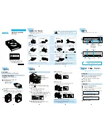
Page 48: ...Specifications 2 12 C156 E205 01EN Figure 2 3 Example of alternate processing ...

Page 49: ...ironmental requirements specified in Subsection 2 1 3 For the temperature of each surface during operation the contact temperature at each measurement point shown in Figure 3 1 must satisfy the requirements specified in Subsection 3 1 2 Low temperature burns The surface temperatures of some ICs on the printed circuit board unit in the optical disk drive exceed 55 C while operating Be careful of lo...

Page 50: ...05 01EN a Inside optical disk cartridge b IC controller read amp Hole for inserting thermocouple Tip of thermocouple Operating of inner partition wall IC controller IC read amp IC power amp Figure 3 1 Surface temperature measurement points ...

Page 51: ...h the hole at the cartridge case and assemble the cartridge disk When there is a gap between the hole and the thermocouple fill the gap with the adhesive agent Note The surface of the cartridge shown in Figure 3 1 has been cut away to make the elements inside the case clearly visible In reality the surface is not cut away If the external environment temperature is higher than the specified value t...

Page 52: ... the temperature surrounding the equipment was kept at 45 C using that at 25 C They are not the same as the data obtained from measurements using the exclusive box in which the equipment is normally used 2 When using the box the ambient temperature around the equipment will differ depending on the air circulation conditions of the box and the temperature rise inside the cartridge will differ becau...

Page 53: ...3 2 Mounting Requirements C156 E205 01EN 3 5 3 2 Mounting Requirements 3 2 1 External dimensions Figures 3 2 to 3 3 show the dimensions of the drive and the positions of the mounting holes ...

Page 54: ...Installation Requirements 3 6 C156 E205 01EN Unit mm Figure 3 2 Dimensions ...

Page 55: ...3 2 Mounting Requirements C156 E205 01EN 3 7 Unit mm Figure 3 3 Dimensions without panel ...

Page 56: ...he permissible installation directions for this drive The mounting angle tolerance must be within 5 to 10 from the horizontal shows that the insertion faces below Eject button Busy LED Disk insertion slot Manual eject hole Figure 3 4 Installation directions Horizontal Vertical Two orientations ...

Page 57: ...3 2 Mounting Requirements C156 E205 01EN 3 9 3 2 3 Centers of gravity Figure 3 5 shows the centers of gravity of the drive Figure 3 5 Centers of gravity ...

Page 58: ...of the drive frame and the user s frame structure must be at least 1 5 mm d The clearance between the top and bottom surfaces and the user s frame structure must be at least 1 5 mm e When mounting the optical disk drive the screw tightening torque should be 0 4 to 0 45Nm 4 to 4 6kgcm f When the optical disk drive with panel is mounted in a locker there should be no deformation of the mounting fitt...

Page 59: ...learance Figure 3 7 Service clearance 4 External magnetic fields Mount the optical disk drive away from powerful magnetic materials e g a speaker to avoid influence from magnetic fields 5 Leak magnetic field The VCM drive magnetic circuit may leak the magnetic field Maximum 25 mT at distance of 4 mm from the drive Do not place a device sensitive to a magnetic field near the optical disk drive 6 Ex...

Page 60: ... frames the metal frame and the plastic nonconductive material frame When using a plastic frame there is not a short circuit between FG of PC and FG of the optical disk drive As a result the static electricity tolerance decreases compared with metal frame It is recommended to use a metal frame to enhance the static electricity prevention 3 3 Power Supply Requirements 1 Allowable input voltage and ...

Page 61: ...has connectors Figure 3 9 shows the location of the connectors AT interface connector 40 pin and power supply connector 4 pin Figure 3 9 Connector and terminal locations Power supply connector 1 12 VDC or not connected 2 12 VDC RETURN GND or not connected 3 5 VDC RETURN GND 4 5 VDC 4 pin 1 pin 2 pin CN1 1 pin CNH5 ...

Page 62: ...e socket Through end type FCN 707B040 AU 0 Fujitsu Signal cable 445 248 40 SPECTRS STRIP Power cable Cable socket housing 1 480424 0 AMP Contact 170121 4 AMP Signal cable AWG18 The host interface cable must be a flat cable in terms of its overall length Do not use a cable with a flat crimp terminal and loose lines or twisted pairs 3 4 3 Drive connection Figure 3 10 is a diagram showing cable conne...

Page 63: ...jumper settings at factory shipping CNH5 3 1 Short 5 6 short circuited Sets the master device 4 2 5 6 Figure 3 11 Jumper settings at factory shipping 3 5 2 Mode setting 1 Setting master device mode Figure 3 12 shows the setting for recognizing the master device device 0 CNH5 3 1 4 2 5 6 Figure 3 12 Master device setting ...

Page 64: ...e In the example shown in Figure 3 15 this setting requires a special interface connection CNH5 3 1 4 2 5 6 Figure 3 14 Cable select mode setting Figure 3 15 shows a cable select example using a special interface cable This example connects CSEL of the master device to the CSEL line conductor of the cable then grounds it so that the drive recognizes that it is the master At this time the CSEL cond...

Page 65: ...r Settings C156 E205 01EN 3 17 Host system Master device Slave device CSEL conductor Open GND Host system Slave device Master device CSEL conductor Open GND Example 1 Example 2 Figure 3 15 Cable select examples ...

Page 66: ...hen handling the drive hold both sides of the mounting frame When touching other than both sides of the mounting frame avoid putting force 5 Do not forcibly push up the end of the header pin of the printed circuit board unit when handling or setting the drive 2 Unpacking a Make sure that the UP label on the package is pointing upward and start unpacking on a level surface Handle the drive on a sof...

Page 67: ...e power supply beforehand Before moving the drive remove the optical disk cartridge If the drive is moved with the optical disk cartridge loaded in it the head may move back and forth in the drive to damage the head or disk and reading the data may fail 4 Packing a Before packing remove the optical cartridge b Store the drive in an antistatic plastic bag with desiccant silica gel c Use the same cu...

Page 68: ... drive packed in principle with the UP sign upward b After unpacking minimize the transportation distance and use cushions to avoid shock and vibration Transport the drive in one of the orientations described in Subsection 3 2 2 after unpacking The horizontal direction is recommended 6 Storage a Use moistureproof packaging when storing the drive b The storage environment must satisfy the requireme...

Page 69: ... the bottom Use mounting screws whose lengths are 3 mm or less from the external wall of the mounting frame of the drive when they are tightened See Figure 3 6 When mounting with screws the screw tightening torque should be 0 4 to 0 45Nm 4 to 4 6kgfcm Be careful not to damage the parts on the PCA when mounting the drive 2 After securing the drive make sure that the drive does not touch the chassis...

Page 70: ...eration when the power is turned on When the power is turned on the drive starts initial self diagnosis The LED on the front panel is on for 1 second during initial self diagnosis If an error is detected during initial self diagnosis the LED on the front panel blinks In case of not inserted the cartridge when the power is turned on the eject motor automatically turns once 2 Checks if errors occur ...

Page 71: ...If processing terminates abnormally a If sense data has been obtained by the REQUEST SENSE command analyze the sense data If the error is recoverable retry the processing b Check the following items for AT interface cable connection All connectors including other devices are connected correctly Make sure the correct cable is being used whether it corresponds with the cable selection mode c Make su...

Page 72: ...equirements 3 24 C156 E205 01EN 4 Remove the four screws securing the drive then remove the drive from the system cabinet 5 When storing or transporting the drive put the drive into an antistatic bag See Section 3 6 ...

Page 73: ...4 1 CHAPTER 4 Host Interface This chapter describes host interface specification 4 1 Pin Assignment 4 2 Signal Description 4 3 Interface Registers 4 4 Various Processes 4 5 ATA Commands 4 6 Packet Commands 4 7 Timing ...

Page 74: ...5 Data bus bit 10 8 DD10 Data bus bit 4 9 DD4 Data bus bit 11 10 DD11 Data bus bit 3 11 DD3 Data bus bit 12 12 DD12 Data bus bit 2 13 DD2 Data bus bit 13 14 DD13 Data bus bit 1 15 DD1 Data bus bit 14 16 DD14 Data bus bit 0 17 DD0 Data bus bit 15 18 DD15 Ground 19 Ground keypin 20 Reserved DMA Request 21 DMARQ Ground 22 Ground I O Write Stop during Ultra DMA data bursts 23 DIOW STOP Ground 24 Groun...

Page 75: ... 27 IORDY DDMARDY DSTROBE Cable Select 28 CSEL DMA Acknowledge 29 DMACK Ground 30 Ground Interrupt Request 31 INTRQ 16 Bit I O 32 IOCS16 Device Address Bit 1 33 DA1 PASSED DIAGNOSTICS Cable assembly type identifier 34 PDIAG CBLID Device Address Bit 0 35 DA0 Device Address Bit 2 36 DA2 Chip Select 0 37 CS0 Chip Select 1 38 CS1 Device Active or Slave Device 1 Present 39 DASP Ground 40 Ground ...

Page 76: ... out transfer 27 IORDY DDMARDY DSTROBE O This is the ready signal for the host computer The ODD uses this signal to request an extension of the transfer cycle when it cannot prepare a response to a data transfer request from the host computer in time Indicates that the ODD can receive Ultra DMA data at Ultra DMA out transfer The host latches data at both edges of this signal at Ultra data in trans...

Page 77: ...mmand block register 38 CS1 O Select signal used to select the control block register 39 DASP I O When reset slave device 1 output signal indicating that the slave device 1 exists Otherwise the signal indicates that the master device 0 and slave device 1 is performing mechanical operation or a failure occurred 2 19 22 24 26 30 40 Ground Ground signal ...

Page 78: ...pedance state Ineffective N A 1 1 0 Alternate Status Device Control N A 1 1 1 Drive Address Ineffective Command block register A N 0 0 0 Data A N 0 0 1 Error ATA Features ATA ATAPI Features ATAPI A N 0 1 0 Sector Count ATA ATAPI Interrupt Reason ATAPI Ineffective A N 0 1 1 Sector Number A N 1 0 0 Cylinder Low ATA ATAPI Byte Count bits 0 7 ATAPI A N 1 0 1 Cylinder High ATA ATAPI Byte Count bits8 15...

Page 79: ...after the command is written in this register For executable commands and required parameters see Table 4 38 4 3 1 3 Data register The data register is used for data transfer The data width is always 16 bits 4 3 1 4 Device Control register This register s bits are defined as shown below Table 4 5 Bit definitions of Device Control register 7 6 5 4 3 2 1 0 Reserved Reserved Reserved Reserved Reserve...

Page 80: ...ts 3 to 0 of the drive select register nDS1 is the device select bit for device 1 It is 0 when device 1 is selected nDS0 is the device select bit for device 0 It is 0 when device 0 is selected 4 3 1 6 ATAPI Byte Count register This register s bits are defined as shown below Table 4 7 Bit definitions of ATAPI Byte Count register 7 6 5 4 3 2 1 0 Byte Count Bits 7 0 R W Byte Count Bits 15 8 R W This ...

Page 81: ...mand The value of this register is effective when the ERR bit of the Status register is 1 at completion of a command other than EXECUTE DEVICE DIAGNOSTIC The value of this register indicates the diagnostic code at power on reset and execution of the EXECUTE DEVICE DIAGNOSTIC command For details on diagnostic codes see Section 4 5 3 Table 4 9 Bit definitions of Error register 7 6 5 4 3 2 1 0 Sense ...

Page 82: ...lue set in this bit When DMA is 1 the ODD performs DMA transfer for data transfer 4 3 1 11 ATA Sector Count register This register is used for the SET FEATURES command 4 3 1 12 ATAPI Interrupt Reason register This register s bits are defined as shown below Table 4 11 Bit definitions of ATAPI Interrupt Reason register 7 6 5 4 3 2 1 0 Reserved Reserved Reserved Reserved Reserved REL I O C D Read Bit...

Page 83: ...r and all other command block registers are ineffective While the ODD is in sleep mode the ATAPI Status register and all other command block registers are ineffective If the host reads this register during interrupt pending the interrupt is cleared Table 4 13 Bit definitions of ATAPI Status register 7 6 5 4 3 2 1 0 BSY DRDY Reserved SERV DRQ Reserved Reserved CHK Read Bit 5 2 and 1 are reserved Th...

Page 84: ...sued it remains set until the ODD completes the internal reset process DRDY Device Ready is always 1 except at the time after reset is made until the next command is issued For SERV set the same value as that of DRDY The SERV bit should be ignored from the standpoint of compatibility DRQ Data Request indicates that the ODD can transfer one byte or one word to or from the host When DRQ is 1 the ATA...

Page 85: ...The device driver should not use the SRST bit to reset the ODD except for restore from sleep mode After ATA software reset the ODD initializes the task file as shown below Status 00h Error Depending on the SRST sequence Sector Count 01h Sector number 01h Cylinder Low 14h Cylinder High EBh Drive Head 00h DRDY is set to 1 with the first command after ATA reset If ATA software reset is issued while t...

Page 86: ...mand the Identify Device command or the Read Sector s command is received the DEV bit is not changed 4 4 3 Defect sector management Sector mapping is executed based on the ISO IEC 10090 standard for 128 MB media the ISO IEC 13963 standard for 230 MB media the ISO IEC 15041 standard for 540 and 640 MB media and Cherry Book for 1 3 GB media the Cherry Book 2 for 2 3GB media Basically possibly defect...

Page 87: ... plural segments and contains write data of plural segments 4 4 5 2 Read cache The ODD enables the read ahead cache and LRU cache when the cache function is enabled When the read cache is enabled the ODD contiguously pre reads the specified sector then pre reading the next sector when receiving a READ command called Read command in this document While pre reading the next sector the ODD transfers ...

Page 88: ...ite cache is enabled the ODD responds to the host with command end This occurs when the data transfer is done with the WRITE command or WRITE AND VERIFY command hereafter Write command in this document The ODD writes data kept in the buffer to media under the following conditions When the Eject switch is pressed When the SYNCHRONIZE CACHE command is received When the FLUSH CACHE command is receive...

Page 89: ...y Immediate command 4 4 7 1 Power mode The ODD supports power modes shown below The ODD uses a power mode equivalent to standby mode except that the DRDY bit is 0 while media is not mounted Active mode Pre idle mode Idle mode Standby mode Sleep mode 4 4 7 2 Active mode In active mode all circuits are enabled The ODD requires the shortest time to start processing a command 4 4 7 3 Pre idle mode In ...

Page 90: ...andard The ODD automatically enters standby mode from active mode if no command is issued within a specified time when the standby timer is enabled When it receives a command the ODD automatically returns active mode The Standby Immediate command can also directly shift the ODD from active or idle mode to standby mode 4 4 7 6 Sleep mode Sleep mode uses power consumption as standby mode To set the ...

Page 91: ...de with the Standby Immediate command and standby timer 4 The ODD enters active mode because it receives a media access command 5 The ODD enters sleep mode with the Sleep command Figure 4 1 Power mode 4 4 8 Unsupported functions The ODD does not support the following functions which are covered by the ATA ATAPI 5 standard Overlapped feature set Queued feature set Advance Power Management feature s...

Page 92: ...arting the download only firmware 1 Blinking on for 0 1 second and off for 0 1 second repeatedly A power on diagnostics error occurred Blinking on for 0 4 seconds and off for 0 4 seconds repeatedly A thermal alarm occurred Blinking on for 0 1 second and off for 0 3 seconds repeatedly An error occurred during writing to the WRITE cache 2 1 The ODD control firmware is stored on the flash ROM and can...

Page 93: ...ESET 08h D 4 5 2 ND EXECUTE DEVICE DIAGNOSTIC 90h D 4 5 3 ND FLUSH CACHE E7h y y y D 4 5 4 ND GET MEDIA STATUS DAh D 4 5 5 PI IDENTIFY PACKET DEVICE A1h D 4 5 6 ND IDLE IMMEDIATE E1h D 4 5 7 ND NOP 00h y 4 5 8 PACKET A0h y y y y D 4 5 9 ND SET FEATURES EFh y y D 4 5 10 ND SLEEP E6h D 4 5 11 ND STANDBY IMMEDIATE E0h D 4 5 12 RESERVED Other codes Notes 1 y This register contains parameters effective...

Page 94: ... X X X SC X X X X X X X X FR X X X X X X X X The CHECK POWER MODE command sets the ODD power mode status in the SC register then notifies the host of the value in Table 4 19 When the drive is in sleep mode the interface is inactive and the ODD cannot receive this command Table 4 19 Power mode indication Power mode status SC register Standby mode 00h Entering standby mode 00h Returning from standby...

Page 95: ...mand resets the ODD When the ODD receives the DEVICE RESET command it sets the BSY bit to 1 After reset is completed the ODD sets the BUSY bit to 0 INTRQ is not asserted 4 5 3 EXECUTE DEVICE DIAGNOSTIC 90h Table 4 21 EXECUTE DEVICE DIAGNOSTIC command Bit 7 6 5 4 3 2 1 0 CM 1 0 0 1 0 0 0 0 DH X X X X X X X X CH X X X X X X X X CL X X X X X X X X SN X X X X X X X X SC X X X X X X X X FR X X X X X X ...

Page 96: ...IAG signal within this time the ODD recognizes that the device 1 self diagnostic test ends successfully Otherwise the ODD recognizes that the device 1 self diagnostic test ended abnormally and the ODD makes OR operation to its self diagnostics results of unit 0 Device 0 with 80h and sets it in the Error register If device 1 ends abnormally the ODD sets the CHECK bit of the Status register When the...

Page 97: ... cache memory in the data buffer to the media 4 5 5 GET MEDIA STATUS DAh Table 4 24 GET MEDIA STATUS command Bit 7 6 5 4 3 2 1 0 CM 1 1 0 1 1 0 1 0 DH X X X DEV X X X X CH X X X X X X X X CL X X X X X X X X SN X X X X X X X X SC X X X X X X X X FR X X X X X X X X The GET MEDIA STATUS command respond with the ODD status The command ends abnormally in either of the conditions given below and sets th...

Page 98: ...this command is received while the media status notification function is disabled this command responds with the ODD status assuming that the media status notification function is enabled Subsequently this command operates assuming that the media status notification function is enabled until it is set to disabled 4 5 6 IDENTIFY PACKET DEVICE A1h Table 4 26 IDENTIFY PACKET DEVICE command Bit 7 6 5 ...

Page 99: ...8 Device type 00000b Direct access unit 7 Replaceable media device 1b 6 5 CMD DRQ type 10b Accelerated DRQ 4 2 Reserved 1 0 Command packet size B 00 12 bytes 1 9 0000h Reserved 10 19 xxx xxx Base serial number Left justified ASCII codes 20 22 0000h Reserved 23 26 aaab Firmware version number aaa Major level version number 000 999 b Minor level version number 0 9 a z and A Z Left justified ASCII co...

Page 100: ...ansfer modes 2 to1 are supported 1b 1 Multiword DMA transfer modes 1 and 0 are supported 1b 0 Multiword DMA transfer modes 0 is supported 1b 64 0003h 15 2 Reserved 0b 1 PIO transfer modes 4 and under are supported 1b 0 PIO transfer modes 3 and under are supported 1b 65 0078h 120 Minimum multiword DMA transfer time per word ns 66 0078h 120 Recommended multiword DMA transfer time ns 67 0078h 120 Min...

Page 101: ... 9 DEVICE RESET command 1b 8 SERVICE command interrupt 0b 7 Interrupt at release 0b 6 Read ahead cache 1b 5 Write cache 1b 4 Packet command function 1b 3 Power management function 1b 2 Removable media function 0b 1 Security mode 0b 0 SMART function 0b 83 4010h Command set supported A value of less than 1 indicates that the command is supported 15 0b 14 1b 13 8 Reserved 0b 7 SET MAX security 0b 6 S...

Page 102: ...rrupt at release is enabled 0b 6 Read ahead cache is enabled 1b Default value 5 Write cache is enabled 1b Default value 4 Packet command function support 1b 3 Power management function support 1b 2 Removable media function support 0b 1 Security mode enabled 0b 0 SMART function is enabled 0b 86 0000h Default value Command set supported and whether the function is enabled or disabled A value of less...

Page 103: ... mode 2 is selected 9 Ultra DMA transfer mode 1 is selected 8 Ultra DMA transfer mode 0 is selected 7 5 Reserved 0b 4 Ultra DMA transfer modes 4 or under are supported 0b 3 Ultra DMA transfer modes 3 or under are supported 0b 2 Ultra DMA transfer modes 2 or under are supported 1b 1 Ultra DMA transfer modes 1 or under are supported 1b 0 Ultra DMA transfer modes 0 is supported 1b 89 92 0000h Reserve...

Page 104: ... 126 0000h Reserved 127 0001h 15 2 Reserved 0b 1 0 Media status notification function supported 01b 128 0000h 15 9 Reserved 0b 8 Security level 0b 7 6 Reserved 0b 5 Extended security erase supported 0b 4 Security count invalid 0b 3 Security freeze 0b 2 Security lock 0b 1 Security valid 0b 0 Security supported 0b 129 254 0000h Reserved 255 0000h 15 8 Cheek some Unused 7 0 Signature Unused ...

Page 105: ... SC X X X X X X X X FR X X X X X X X X The ODD sets the power mode to idle mode 4 5 8 NOP 00h Table 4 29 NOP command Bit 7 6 5 4 3 2 1 0 CM 0 0 0 0 0 0 0 0 DH X X X DEV X X X X CH X X X X X X X X CL X X X X X X X X SN X X X X X X X X SC X X X X X X X X FR X X X X X X X X The NOP command enables 16 bit access for Status register checking The ODD judges an unsupported command The command ends with A...

Page 106: ...X X X X X FR X X X X X X X X The PACKET command issues the ATAPI packet command For the Byte Count Limit specify the maximum number of bytes transferred per INTRQ in PIO mode When the value of the Byte Count Limit is smaller than 2048 the data is transferred in 2048 byte units The execution protocol of the ATAPI packet command conforms to the AT Attachment with Packet Interface 5 ATA ATAPI 5 of th...

Page 107: ...rts Aborted Command Table 4 32 FR register setting value Setting value Function Default value 02 Enables the write cache 03 Supports data transfer depending on the value of the SC register See Table 4 33 31 31 Disables the media status notification function 55 Disables the read ahead cache 66 Does not reset various setting values to the power on default value by software reset The media status not...

Page 108: ...ltiword DMA transfer mode 00100 Mode Ultra DMA transfer mode 01000 Mode Undefined 10000 Mode indicates the number of transfer modes When the FR register is 95h the ODD responds with the following value at the end of the command Table 4 34 Cylinder Low register Bit 7 Bit 6 Bit 5 Bit 4 Bit 3 Bit 2 Bit 1 Bit 0 Version 00h Table 4 35 Cylinder High register Bit 7 Bit 6 Bit 5 Bit 4 Bit 3 Bit 2 Bit 1 Bit...

Page 109: ...leep mode by following the steps given below 1 The ODD spins down media 2 The ODD issues an interrupt to the host to report command end After the host receives the interrupt the ODD deactivates the interface Once the interface becomes inactive the ODD ignores all resets except software reset and hardware reset and Device Reset command A software reset or hardware reset or Device Reset command is r...

Page 110: ... IMMEDIATE E0h Table 4 37 STANDBY IMMEDIATE command Bit 7 6 5 4 3 2 1 0 CM 1 1 1 0 0 0 0 0 DH X X X DEV X X X X CH X X X X X X X X CL X X X X X X X X SN X X X X X X X X SC X X X X X X X X FR X X X X X X X X The ODD sets the power mode to standby mode ...

Page 111: ...E SENSE 10 5Ah 4 6 7 PREVENT ALLOW MEDIUM REMOVAL 1Eh 4 6 8 READ 10 28h 4 6 9 READ CAPACITY 25h 4 6 10 READ FORMAT CAPACITIES 23h 4 6 11 READ DEFECT DATA 10 37h 4 6 12 READ DEFECT DATA 12 B7h 4 6 13 READ LONG 3Eh 4 6 14 RECEIVE DIAGNOSTIC RESULTS 1Ch 4 6 15 REQUEST SENSE 03h 4 6 16 SEND DIAGNOSTIC 1Dh 4 6 17 SEEK 10 2Bh 4 6 18 START STOP UNIT 1Bh 4 6 19 SYNCHRONIZE CACHE 35h 4 6 20 TEST UNIT READY...

Page 112: ...k Condition is returned 4 6 1 ERASE command Table 4 39 ERASE command Bit Byte 7 6 5 4 3 2 1 0 0 Operation Code 2Ch 1 Reserved 2 5 Logical Block Address 6 Reserved 7 8 Transfer Length 9 11 Reserved The ERASE command erases data of the specified number of blocks from the specified logical block address Logical Block Address specifies the head logical block address from which the ODD starts writing T...

Page 113: ... transferred Defect List Format is ignored When the FmtData bit is 0 the ODD does not transfer the FORMAT UNIT parameter list and formats media using the internal default values instead The CmpList is ignored The interleaving is set to the internal default value even if a value is specified Table 4 41 FORMAT UNIT parameter list Bit Byte 7 6 5 4 3 2 1 0 0 3 Defect List Header Table 4 42 Defect list...

Page 114: ...s completed Defect List Length must be 0 If any other value is set the command assumes as 0 is specified 4 6 3 INQUIRY command Table 4 43 INQUIRY command Bit Byte 7 6 5 4 3 2 1 0 0 Operation Code 12h 1 Reserved 2 Reserved 3 Reserved 4 Allocation Length 5 11 Reserved The INQUIRY command transfers device information to the host If the INQUIRY command is issued while the ODD contains the Unit Attenti...

Page 115: ... is filled with space characters 20h 16 31 Products Identification MCJ3230AP in ASCII Left justified The rightmost data field not used is filled with space characters 20h 32 35 Firmware Revision Level 0000 999z in ASCII 36 Firmware Local Revision 00h FFh in HEX 37 Boot Firmware Revision Level 00h FFh in HEX 38 39 Signature MO in ASCII 40 47 Factory infomation The Factory Information is the data fo...

Page 116: ...ages bit is 1 the ODD saves all parameter values transferred to the flash ROM Parameter List Length specifies the number of bytes in the mode parameters to be transferred If it is 0 the command does not carry out transfer and ends normally If the transferred mode parameters are insufficient the command responds with Check Conditions Table 4 46 lists mode parameters supported Table 4 46 Mode parame...

Page 117: ...8 lists the mode parameter header Table 4 48 Mode parameter header Bit Byte 7 6 5 4 3 2 1 0 0 Mode Data Length 1 Medium Type Code 2 WP Reserved 3 Block Descriptor Length The values specified for Mode Data Length Medium Type Code and WP are ignored Block descriptor Length must be 0 or 8 Table 4 49 lists the block descriptors All the values specified for Block Descriptor are ignored Table 4 49 Block...

Page 118: ...block assignment is made for the WRITE 10 or WRITE AND VERIFY command When the bit of AWRE is 1 automatic alternate block assignment is made When the RC Read Continuous bit is 0 the command reports an error if an uncorrectable data error is detected in the READ 10 command When the bit of RC is 1 the command transfers the wrong data and ends normally even if an uncorrectable error is detected When ...

Page 119: ...en the bit of DCR is 1 the command does not correct errors even if a correctable error is detected Read Retry Count must not be 3 or smaller If a value of 3 or smaller is specified the command assumes 4 and reports Recovered Error Write Retry Count must not be a value other than 3 If a value other than 3 is specified the command assumes 3 and reports Recovered Error To assure media compatibility t...

Page 120: ...ation A device driver should not be used this page because if device driver uses of this page and it is not able to keep compatibility for logically of media No guarantee Transfer Rate defines kbits sec Number of Heads Sectors per Track and Number of Cylinders define logical value It does not show physical numbers No guarantee for logical compatibility of media when device driver or application is...

Page 121: ...8 29 0000h 30 31 00h Table 4 56 Default values in flexible disk page Bit Byte 7 6 5 4 3 2 1 0 2 3 3E80h 4 40h 5 20h 6 7 In case of 640 Mbytes 1 3 Gbytes and 2 3 Gbytes media 800h Others or Not Ready 200h 8 9 Number of LBA for media 40h 20h In case of Not Ready the value of the maximum capacity media among the supported 512 sectors media 10 19 00h 20 FFh 21 27 00h 28 29 1194h 30 31 00h ...

Page 122: ...RIFY command is disabled When the bit of WCE is 1 the write cache function is enabled When the RCD Read Cache Disable bit is 0 the read ahead cache function for the READ 10 command is enabled When the bit of RCD is 1 the read ahead cache function is disabled The caching page can be saved Table 4 58 Changeable values in the caching page Bit Byte 7 6 5 4 3 2 1 0 2 0 0 0 0 0 1 0 1 3 19 00h Table 4 59...

Page 123: ...erates in accordance with the default timer value in the ODD When the Standby bit is 1 specify the time after the device enters idle mode until it enters standby mode The Idle Condition Timer value and the Standby Condition Timer value are specified with a value in 100 ms units If the value specified for the Standby Condition Timer is not a multiple of 600 258h the ODD automatically rounds down th...

Page 124: ... Visual Mode AV bit is 0 the cache mode is applied When the AV bit is 1 the AV data support mode is applied When the Streaming Mode SM bit is 0 the test write operation may interrupt the read or write operation When the SM bit is 1 the test write operation is restricted during the read or write operation We recommend setting 0 for the SM bit The Verify Mode VM specifies the verify operation for th...

Page 125: ... 4 65 Verify Control Page variable Bit Byte 7 6 5 4 3 2 1 0 2 1 1 0 11b 3 0 1Fh 4 7 0 Table 4 66 Verify Control Page default value Bit Byte 7 6 5 4 3 2 1 0 2 1 0 0 00b 3 0 0h 4 7 0 4 6 5 Mode Select 10 command Table 4 67 Mode Select 10 command Bit Byte 7 6 5 4 3 2 1 0 0 Operation Code 55h 1 Reserved PF Reserved SP 2 6 Reserved 7 8 Parameter List Length 9 11 Reserved The MODE SELECT 10 command perf...

Page 126: ...s The Mode Parameter List consists of the Mode Parameter Header the Block Descriptor and the Mode Page Table 4 69 shows the mode parameter header Table 4 69 Mode Parameter Header Bit Byte 7 6 5 4 3 2 1 0 0 1 Mode Data Length 2 Medium Type Code 3 WP Reserved 4 5 Reserved 6 7 Block Descriptor Length The values specified for the Mode Data length the Medium Type Code and the WP are ignored For the Blo...

Page 127: ...be transferred When the Allocation Length is 0 this command is terminated normally without transferring data The Page Control PC specifies the type of the Page to be transferred Table 4 71 Page Control field Bit 7 Bit 6 Parameter type 0 0 Current value 0 1 Changeable value 1 0 Default value 1 1 Saved value Page Code specifies the Mode Page to be transferred If Page Code is 3Fh all Mode Pages are t...

Page 128: ...5 4 3 2 1 0 0 Mode data Length 1 Medium Type Code 2 WP Reserved 3 Block Descriptor Length Medium Type Code returns the following values 03h for non overwrite 07h for overwrite 03h for other media and Not Ready state The WP Write Protect bit indicates the state of the write protect key on the cartridge A value of 1 indicates write protected Mode Data Length indicates the length of mode data to be t...

Page 129: ... inserted If not 0 is returned Table 4 75 shows the mode page format Table 4 75 Mode Page Format Bit Byte 7 6 5 4 3 2 1 0 0 PS 0 Page Code 1 Page length n 1 2 n Reserved A value of 1 in PS indicates that the page descriptor can be saved on the Flash ROM 4 6 7 MODE SENSE 10 command Table 4 76 MODE SENSE 10 command Bit Byte 7 6 5 4 3 2 1 0 0 Operation Code 5Ah 1 Reserved DBD Reserved 2 PC Page Code ...

Page 130: ...der 0 7 Block Descriptor 0 n Mode Page s The Mode Parameter List consists of the Mode Parameter Header the Block Descriptor and the Mode Page Table 4 7 8 shows the mode parameter header Table 4 78 Mode Parameter Header Bit Byte 7 6 5 4 3 2 1 0 0 1 Mode Data Length 2 Medium Type Code 3 WP Reserved 4 5 Reserved 6 7 Block Descriptor Length For an explanation of each field of the Mode Parameter Header...

Page 131: ...riting on media then allows ejection Hard reset resets the prevent state to allow ejection Table 4 80 Response to Prevent Allow Eject Operation Status at operation When no media is loaded When media is loaded Prevent 0 Enabled No error No error Inhibited No error No error Prevent 1 Enabled No error No error Media ejection is inhibited Inhibited No error No error Eject Enabled No error No error Eje...

Page 132: ...block address used to start reading Transfer Length specifies the number of blocks to be read and transferred When Transfer Length is 0 the command does not carry out data transfer It simply ends normally without reading any data 4 6 10 READ CAPACITY command Table 4 82 READ CAPACITY command Bit Byte 7 6 5 4 3 2 1 0 0 Operation Code 25h 1 Reserved 2 7 Reserved 8 Reserved PMI 9 11 Reserved The READ ...

Page 133: ...ES command Bit Byte 7 6 5 4 3 2 1 0 0 Operation Code 23h 1 Reserved 2 6 Reserved 7 8 Allocation Length 9 11 Reserved The READ FORMAT CAPACITIES command transfers data on the capacity of media currently loaded to the host If no media is loaded this command returns the maximum capacity value of supported media to the host Table 4 85 READ FORMAT CAPACITIES data format Bit Byte 7 6 5 4 3 2 1 0 Capacit...

Page 134: ... to be reported to the host Block Length indicates the length of the block in bytes Table 4 88 Descriptor code definition Descriptor Code Descriptor Type 00b Unformatted media Other fields are ineffective 01b Unformatted media Maximum format capacity 10b Formatted media Current media capacity 11b No media loaded Maximum format capacity 4 6 12 READ DEFECT DATA 10 command Table 4 89 READ DEFECT DATA...

Page 135: ...ed the command assumes 101b and reports Recovered Error Table 4 90 Defect List Format READ DEFECT DATA 10 Defect List Format Data format 101 Physical sector address format Up to 8191 in the defect list 111 Physical sector address format 8192 or later in the defect list Table 4 91 shows the defect list header Table 4 92 shows the defect descriptors Table 4 91 Defect List Header READ DEFECT DATA 10 ...

Page 136: ...mand transfers header and PDL When Glist is 1 the command transfers header and SDL When both Plist and Glist are 0 the command transfers the header When both Plist and Glist are 1 the command transfers PDL and SDL PDL and SDL are respectively arranged in an ascending order The defect list format supported is listed in Table 4 95 Defect List Format READ DEFECT DATA 12 If any other format is specifi...

Page 137: ...READ LONG command Table 4 97 READ LONG command Bit Byte 7 6 5 4 3 2 1 0 0 Operation Code 3Eh 1 Reserved 2 5 Logical Block Address 6 Reserved 7 8 Byte Transfer Length 9 11 Reserved The READ LONG command reads data in the data CRC and ECC sections from the specified logical block address The transfer byte length must be a multiple of 600 258h bytes for 512 byte media and a multiple of 2380 94Ch byte...

Page 138: ...command transfers no data and ends normally 4 6 16 REQUEST SENSE command Table 4 99 REQUEST SENSE command Bit Byte 7 6 5 4 3 2 1 0 0 Operation Code 03h 1 Reserved 2 3 Reserved 4 Allocation Length 5 11 Reserved The REQUEST SENSE command transfers sense data to the host Sense data indicates detailed error information on the command whose error was reported previously If no error command was reported...

Page 139: ...r Code 70h or 71h 1 Reserved 00h 2 Reserved 0h Sense Key 3 6 Information 7 Additional Sense Length 18h 8 11 Command Specific Information 12 Additional Sense Code 13 Additional Sense Code Qualifier 14 Reserved 00h 15 17 Sense key specific 18 31 Additional Sense Bytes When the Valid bit is 1 the information field bytes 3 to 6 is effective Error Code indicates the sense data format and type See Table...

Page 140: ...to hardware failure 5h ILLEGAL REQUEST Indicates that command packets or command parameters contains invalid data Media data remains unchanged 6h UNIT ATTENTION Indicates that reset power on or media exchange is caused 7h DATA PROTECT Indicates that media is write protected with the Write Protect key or the device is softwre write protected 8h BLANK CHECK Indicates that a blank sector is detected ...

Page 141: ...LED 3 10 00 ID CRC ERROR 3 11 00 UNRECOVERED READ ERROR 3 15 02 POSITIONING ERROR DETECTED BY READ OF MEDIUM 1 17 06 RECOVERED DATA WITHOUT ECC DATA AUTO REALLOCATED 1 18 00 RECOVERED DATA WITH ERROR CORRECTION RETRIES APPLIED 1 19 00 DEFECT LIST ERROR 3 19 01 DEFECT LIST NOT AVAILABLE 3 19 02 DEFECT LIST ERROR IN PRIMARY LIST 3 19 03 DEFECT LIST ERROR IN SECONDARY LIST 1 1C 00 DEFECT LIST NOT FOU...

Page 142: ...APPED COMMAND ATTEMPTED 4 53 00 MEDIA LOAD OR EJECT FAILED 5 53 02 MEDIUM REMOVAL PREVENTED 4 83 00 THERMAL ERROR The Sense Key Specific field format is shown in Table 4 105 Format Progress Indication Bytes is effective only when Sense key is NOT READY and the SKSV bit is 1 Otherwise the field is set with 00h This field is defined for the FORMAT UNIT command having the Immed bit of 1 Table 4 105 F...

Page 143: ...gnostics on the data buffer If an error occurs the device responds with Check Condition Parameter List Length specifies the data length of diagnostic parameters to be transferred The functions and specifications of diagnostic parameters are not open 4 6 18 SEEK command Table 4 107 SEEK command Bit Byte 7 6 5 4 3 2 1 0 0 Operation Code 2Bh 1 Reserved 2 5 Logical Block Address 6 11 Reserved The SEEK...

Page 144: ...OP UNIT command ejects media or starts and stops rotating the disk When the IMMED Immediate bit is 1 command completion is reported before processing is completed Processing for other values is listed in Table 4 109 Table 4 109 START STOP EJECT processing LoEj Start Processing 0 0 Stops disk rotation 0 1 Starts disk rotation and checks the format type of media 1 0 Ejects media if possible 1 1 Ends...

Page 145: ...ition The command writes all data not written yet in the cache memory of the data buffer to media regardless of the value set in Logical Block Address and Number of Blocks The command does not check the value of Logical Block Address and Number of Blocks 4 6 21 TEST UNIT READY command Table 4 111 TEST UNIT READY command Bit Byte 7 6 5 4 3 2 1 0 0 Operation Code 00h 1 11 Reserved The TEST UNIT READ...

Page 146: ...head logical block address from which verification starts Verification Length specifies the number of blocks to be verified and transferred When Verification Length is 0 the command verifies no block and ends normally The ByteChk bit indicates data compare execution However since the ByteChk is not supported it must be set to 0 If a value 1 is specified the command ends with Check Condition 4 6 23...

Page 147: ...2 1 0 0 Operation Code 2Eh 1 Logical Unit Number Reserved ByteChk Reserved 2 5 Logical Block Address 6 Reserved 7 8 Transfer Length 9 11 Reserved The WRITE AND VERIFY command receives and writes data for the specified number of blocks from the specified logical block address Logical Block Address specifies the head logical block address used to start writing Transfer Length specifies the number of...

Page 148: ...d checks for validity of transfer data then writes it on the flash ROM If TNFY is 0 and Allocation Length is 0 the command checks propriety of data on the data buffer and writes on the flash ROM When TNFY is 1 the command transfers data to be written on the flash ROM into the data buffer Code ID indicates the type of code to be downloaded Allocation Length indicates the length of data to be transf...

Page 149: ...Code 3Fh 1 Reserved 2 5 Logial Block Address 6 Reserved 7 8 Byte Transfer Length 9 11 Reserved The WRITE LONG command writes data in the data CRC and ECC sections to the specified logical block address The transfer byte length must be a multiple of 600 258h bytes for 512 byte media and a multiple of 2380 94Ch bytes for 2048 byte media ...

Page 150: ... 78 C156 E205 01EN 4 7 Timing 4 7 1 Register PIO data transfer timing Figure 4 2 Register PIO data transfer DA 2 0 CS0 CS1 IORDY IOCS16 READ DD 15 0 WRITE DD 15 0 DIOR DIOW t0 t2 t9 t2i t1 t7 t3 t5 t6 t6Z tA tB TRd t4 ...

Page 151: ...DIOR DIOW recovery time 25 t3 DIOW data setup time 20 t4 DIOW data hold time 10 t5 DIOR data setup time 20 t6 DIOR data hold time 5 t6Z DIOR data High Z time 30 t7 From address decided to IOCS16 asserted 30 t8 From address decided to IOCS16 released 30 t9 DIOR DIOW to address valid hold time 10 tA IORDY setup time 35 PIO flow control transfer mode tB IORDY pulse width 1250 PIO flow control transfe...

Page 152: ...nterface 4 80 C156 E205 01EN 4 7 2 Multiword DMA data transfer timing Figure 4 3 Multiword DMA data transfer tM tG tF tG tE tK tD tI tZ tJ tL t0 tN tH CS0 CS1 DMARQ DMACK DIOR DIOW READ DD 15 0 WRITE DD 15 0 ...

Page 153: ...e 2 tD DIOR DIOW pulse width 70 tE DIOR data access time 50 tF DIOR data hold time 5 tG DIOR DIOW data setup time 20 tH DIOW data hold time 10 tI DMACK to DIOR DIOW setup time 0 tJ DIOR DIOW to DMACK hold time 5 tK DIOR DIOW negated pulse width 25 tL DIOR DIOW to DMARQ delay time 35 tM CS 1 0 to DIOR DIOW valid time 25 tN CS 1 0 hold time 10 tZ DMACK to tristate time 25 ...

Page 154: ...ENV tENV tZIORDY tAZ tZAD tZAD tFS tFS tDVS tCVH Figure 4 4 Ultra DMA data in transfer initialization timing 4 7 4 Ultra DMA data in transfer continuous transfer timing DSTROBE at device DD 15 0 at device DSTROBE at device DD 15 0 at device t2CYC tCYC tCYC t2CYC tDVH tDVH tDVH tDVS tDVS tDH tDH tDH tDS tDS Figure 4 5 Ultra DMA data in transfer continuous transfer timing ...

Page 155: ...BE DD 15 0 tRP tSR tRSF Figure 4 6 Ultra DMA data in transfer host stop timing 4 7 6 Ultra DMA data in transfer device end timing DMARQ DMACK STOP HDMARDY DSTROBE DD 15 0 DD 2 0 CS0 CS1 tMLI tLI tLI tLI tSS tACK tACK tIORDYZ tACK tACK tDVH tDVS tZAH tAZ CRC Figure 4 7 Ultra DMA data in transfer device end timing ...

Page 156: ...N 4 7 7 Ultra DMA data in transfer host end timing DMARQ DMACK STOP HDMARDY DSTROBE DD 15 0 DA 2 0 CS0 CS1 tLI tMLI tZAH tAZ tRP tRFS tLI tMLI tACK tACK tIORDYZ tDVS tDVH tACK tACK Figure 4 8 Ultra DMA data in transfer host end timing ...

Page 157: ...ACK tACK tZIORDY tENV tLI tUI tDVS tCVH Figure 4 9 Ultra DMA data out transfer initialization timing 4 7 9 Ultra DMA data out transfer continuous transfer timing HSTROBE at host DD 15 0 at host HSTROBE at host DD 15 0 at host t2CYC tCYC tCYC t2CYC tCVH tCVH tCVH tDVS tDVS tDH tDH tDH tDS tDS Figure 4 10 Ultra DMA data out transfer continuous transfer timing ...

Page 158: ...Host Interface 4 86 C156 E205 01EN 4 7 10 Ultra DMA data out transfer device stop timing DMARQ DMACK STOP DDMARDY HSTROBE DD 15 0 tRP tSR tRFS Figure 4 11 Ultra DMA data out transfer device stop timing ...

Page 159: ...7 4 7 11 Ultra DMA data out transfer host suspend timing DMARQ DMACK STOP DDMARDY HSTROBE DD 15 0 DA 2 0 CS0 CS1 tLI tLI tLI tSS tMLI tMLI tACK tIORDYZ tDVS tDVH tACK tACK Figure 4 12 Ultra DMA data out transfer host suspend timing ...

Page 160: ...EN 4 7 12 Ultra DMA data out transfer device end timing DMARQ DMACK STOP DDMARDY HSTROBE DD 15 0 DA 2 0 CS0 CS1 tMLI tMLI tLI tLI tACK tACK tIORDYZ tDVS tDVH tACK tACK tRFS tRP Figure 4 13 Ultra DMA data out transfer device end timing ...

Page 161: ...bled setup time on sending side 30 tDVH Data enabled hold time 6 tFS First strobe time 0 170 tLI Restricted interlock time 0 150 tMLI Minimum interlock time 20 tUI Non restricted interlock time 0 tAZ Driver Maximum release time 10 tZAH Output delay time 20 tZAD Driver Assert and negate time 0 tENV Envelope time 20 70 tSR STROBE to DMARDY time 20 tRSF Ready to the last STROBE time 60 tRP Ready to s...

Page 162: ...cate that it is in operation when device 1 is not connected 3 DASP is used to indicate that the device is in operation Figure 4 14 Power on and reset timing t10 t18 t17 t16 t15 t14 t13 t12 t11 RESET Device 0 BSY Device 1 DASP out Device 1 DRDY Device 1 BSY Device 0 PDIAG in Device 0 DASP in Device 0 DASP out Device 0 PDIAG out Device 0 DRDY Device 1 PDIAG out ...

Page 163: ... RESET negation to BSY bit set to one release PDIAG 400 ns t12 Device 0 release DASP 1 ms t13 Device 0 sample time of DASP 1 ms 450 ms t14 Device 0 sample time of PDIAG 1 ms 31 s t15 Device 1 RESET negation to BSY bit set to one 400 ns t16 Device 1 assert DASP 400 ms t17 Device 1 negate PDIAG if asserted 1 ms t18 Device 1 assert PDIAG 30 s ...

Page 164: ...This page is intentionally left blank ...

Page 165: ...This section explains loading and ejection methods assuming that the drive is mounted horizontally When mounted vertically the drive is operated in the same manner as when mounted horizontally Figure 5 1 shows the front view of the optical disk drive For operation users should be familiar with the parts in the figure and their function Loading and ejection methods are described below 5 1 Operating...

Page 166: ...l disk cartridge 2 Eject button BUSY LED display lamp On this optical disk drive this is the push button combining the eject button with the BUSY LED display lamp for ejecting the optical disk cartridge it lights in green during seeking and during erasing writing or reading of data When ejection is disabled by the SCSI command the optical disk cartridge cannot be taken out 3 Manual eject hole This...

Page 167: ... is inserted After several seconds the BUSY LED indicator lamp is turned on and immediately turned off to complete loading Notes 1 The cartridge must be completely inserted until the BUSY LED indicator lamp is lit 2 If the cartridge is inserted by pushing either left or right side of the cartridge rear it may not be inserted completely Be sure to push the central part straight into the drive until...

Page 168: ...e central part straight into the drive until it is completely inserted 3 If you attempt to insert the cartridge by force trouble may result in the drive In such a case be sure to once remove the cartridge and check the insertion direction and the face and back of the cartridge before inserting it again Figure 5 2 Inserting cartridge Even if you inserted the optical disk cartridge by pressing the l...

Page 169: ...rtridge s condition 3 Remove the cartridge when completely ejected 2 When the drive power is off If the drive power is off the cartridge cannot be removed by pressing the eject button The cartridge can be removed by insert the eject jig accessory or a pin diameter about 1 mm into the manual eject hole See figure 5 3 Notes 1 NEVER attempt to eject the cartridge while the BUSY LED lamp is on The dat...

Page 170: ... cleaner 020470 CA90002 C980 1 Cleaning method Clean the head actuator with following method 1 Turn on the power of the drive 2 Insert the head cleaner 3 When the head cleaner is automatically loaded the optical head positioner moves back and forth and the cleaning brush mounted on the head cleaner cleans the object lens 4 When the cleaning is finished the head cleaner is automatically unloaded cl...

Page 171: ...cartridge Figure 5 4 shows the optical disk cartridge For operation and cleaning users should be familiar with the parts shown in the figure See Subsection 2 3 2 for the functions of the parts Shutter closed Shutter open Figure 5 4 Optial disk cartridge 3 Write protect tab 1 Cartridge case 2 Shutter 5 Hub 4 Disk ...

Page 172: ...o move the write protect tab it must be completely moved to the end because there is play in the middle Figure 5 5 shows the write protect tab location on the optical disk cartridge and the moving state of the write protect tab see write enabled and write disabled entered on the label Note The hatched part indicates the write protect tab location Figure 5 5 Write protect tab Write protect tab ...

Page 173: ...s done firmly press each corner of the index label b 4 When the front is also complete again press every corner of the index label to prevent the label from coming off c a b c Figure 5 6 How to stick an index label on the MO cartridge 5 3 4 Notes To maintain the performance and reliability of the optical disk cartridge keep the following points in mind when using storing or transporting the cartri...

Page 174: ...exposed to direct sunlight or where the temperature changes sharply the temperature is high or the humidity is high Do not store the cartridge in a dusty or smoky place 3 When transporting the cartridge Put the cartridge in a nylon bag to protect it from moisture Put the cartridge in a strong container and cover the cartridge with cushioning material ...

Page 175: ...g tool Use the cleaning kit to clean the disk cartridge 1 Cleaning kit This cleaning kit is only for 3 5 inch optical disk cartridge Use with reading the attached operation guide well Table 5 2 shows the order number of the cleaning kit Table 5 2 Cleaning kit Part name Product number Order number Cleaning kit 0632440 CA90003 0702 Table 5 3 shows the packed items in the cleaning kit Table 5 3 Packe...

Page 176: ...near the revolving knob Do not use or storage where exposed to direct sun light or near the inflammables Keep out of the reach of children Damage for data medium Do not use this cleaning kit for the floppy disk or the optical disk cartridge used for other optical disk drive 5 4 2 Cleaning procedure Clean the disk cartridge with a following procedure Damage for disk medium Clean the cartridge at cl...

Page 177: ...pply the heavy shock and push hardly 3 Cover the cartridge with the setting case cover then insert the spindle pin into the center hub of the cartridge Figure 5 9 Cleaning procedure 3 4 Remove a slender piece that causes a defect from the disk surface at wiping the disk media 5 Moisten the cleaning cloth with a few drops of cleaning solution Shutter stopped Setting case Setting case as shown Disk ...

Page 178: ...th eyes immediately flush eyes with water 6 Wipe the disk surface from the hub outward 7 Turn the revolving knob then wipe the disk surface Figure 5 10 Cleaning procedure 4 8 If the excess cleaning solution remains on the disk surface wipe out with the cleaning cloth Cleaning cloth ...

Page 179: ...ion can check the basic operations of the drive A test program running in the host system is required to check general operations including operations of the interface with the host system See Subsection 6 1 3 Table 6 1 Self diagnostic function Diagnostic contents Target Initial self diagnosis Basic operation hardware function test Diagnostic command Basic operation Test program General operation ...

Page 180: ...ystem can make the ODD execute the self diagnosis by issuing the EXECUTIVE DEVICE DIAGNOSTIC command See Section 4 7 2 EXECUTIVE DEVICE DIAGNOSTIC in details 6 1 3 Test program A test program running in the host system is required to check general operations such as operations of the interface with the host system and simulated operations The configuration and function of the test program depend o...

Page 181: ...be included a Optical disk drive model part number P N revision number serial number S N and date of manufacture b Failure status Date of the failure System configuration Environment conditions temperature humidity and supply voltage c Failure history d Failure Description of the failure Issued commands and specified parameters Sense data Other error analysis information Data loss In case of regul...

Page 182: ...e lines See Figure 6 2 2 Changing the revision number on site When the revision number is changed on site because of parts replacement or modification the new revision number is indicated by circling the number on the line of alphabetic characters See Figure 6 2 NOTICE When a revision number is changed after shipment Fujitsu issues Revision Number Change Request Notice to indicate the new revision...

Page 183: ...dling and also allows the operator to exchange disks easily The case also contains a label write protection tab automatic handling support and media identification hole CDB Command Descriptor Block A series of data describing input output commands CDB is sent from the initiator to the target Clamp area A ring area on the disk on which a clamp force is applied by the clamp mechanism Command An inpu...

Page 184: ...nges data units so that data resists burst errors LUN Logical Unit Number A device address used to identify a logical unit Recording layer A layer on the disk on which data is recorded at production or recording Recording power An incidence power specified on the incidence surface Used to form marks Sense code A single byte code set in sense data This information is used to determine the type of e...

Page 185: ...Glossary C156 E205 01EN GL 3 Status A single byte information reported from the target to the initiator at the end of each command execution The status indicates the end status of a command ...

Page 186: ...This page is intentionally left blank ...

Page 187: ...isable Block Descripter DBP Data Bus Parity DC Direct Current DCRT Disable CeRTification DDS Disk Definition Sector DMA Defect Management Area DPO Disable Page Out DPRY Disable PRimarY DSP Digital Signal Processor E EBC Enable Blank Check EBP Erase By Pass ECC Error Correction Code EN European Norm EVPD Enable Vital Product Data F FG Frame Ground FIFO First In First Out FmtData Format data FOV For...

Page 188: ...elAdr Relative Addressing REQ REQuest RH Relative Humidity ROM Read only Memory rpm revolutions per minute RST ReSeT RSV ReSerVed S S N Serial Number SB Spare Band SCT SeCTor SDL Secondary Defect List SDTR Synchronous Data Transfer Request SEL SELect SFP Standard Formatted Part SG Signal ground SKSV Sense Key Specific Valid SM Sector Mark SNSKEY SeNSe KEY SP Save Page SP Save Parameter STPF SToP F...

Page 189: ...ition of alternate status register 4 7 Bit definition of ATAPI block device select register 4 9 Bit definition of ATAPI byte count register 4 8 Bit definition of ATAPI feature register 4 10 Bit definition of ATAPI interrupt reason register 4 10 Bit definition of ATAPI status register 4 11 Bit definition of device control register 4 7 Bit definition of drive address register 4 8 Bit definition of e...

Page 190: ...efinition 4 62 Device 1 connected 4 24 Device 1 not connected 4 24 Device control register 4 7 Device damage 3 18 Device driver software 1 5 Device end timing 4 83 4 88 Device parameter information 4 27 to 4 31 DEVICE RESET 4 23 DEVICE RESET command 4 23 Device stop timing 4 86 Diagnosis and maintenance 6 1 Diagnostic command 6 2 Diagnostic function 1 3 Dimension 3 7 Direct overwrite medium suppor...

Page 191: ...20 Logical block address format 4 68 Lower power consumption 1 3 Low temperature burn 3 1 M Maintainability operability 1 3 Maintenance information 6 3 Maintenance requirement 6 3 Master device setting 3 15 Mean time between failures 1 3 2 6 Mechanical section 1 7 Media interchangeability 1 2 Media status notification function 4 16 Model and order number 2 1 Model and product number 2 1 Mode page ...

Page 192: ... 4 Read cache 4 15 READ CAPACITY command 4 60 READ CAPACITY data 4 61 READ DEFECT DATA 10 command 4 62 READ DEFECT DATA 12 command 4 64 READ FORMAT CAPACITIES command 4 61 READ FORMAT CAPACITIES data format 4 61 READ LONG command 4 65 Read write error recovery page 4 46 RECEIVE DIAGNOSTIC RESULTS command 4 66 Recommended optical disk cartridge specification 2 7 Register PIO data transfer 4 78 Regi...

Page 193: ...t 3 3 Temperature rise under several condition 3 4 Test program 6 2 TEST UNIT READY command 4 73 Timing 4 78 Transfer setting value in SC register 4 36 Transportation 3 20 Transporting cartridge 5 10 U Ultra DMA data in transfer 4 82 to 4 84 Ultra DMA data out transfer 4 85 4 87 Ultra DMA data out transfer continuous transfer timing 4 85 Ultra DMA data out transfer parameter 4 89 Unpacking 3 18 Un...

Page 194: ...This page is intentionally left blank ...

Page 195: ... 26294 1 FAX 39 2 26294 201 FUJITSU FRANCE S A 1 Place des Etas Unis SILIC 310 94588 Rungis Cedex FRANCE TEL 33 1 41 80 38 80 FAX 33 1 41 80 38 66 FUJITSU ICL ESPAÑA S A Almagro 40 28010 Madrid SPAIN TEL 34 91 581 8000 FAX 34 91 581 8300 FUJITSU AUSTRALIA LIMITED 2 Julius Avenue Cnr Delhi Road North Ryde N S W 2113 AUSTRALIA TEL 61 2 9776 4555 FAX 61 2 9776 4556 FUJITSU HONG KONG LTD 10 F Lincoln ...

Page 196: ...This page is intentionally left blank ...

Page 197: ...mments Reply requested Yes No Please evaluate overall quality of this manual by marking in the appropriate boxes Good Fair Poor Good Fair Poor Good Fair Poor Organization Use of examples Legibility Accuracy Index coverage Handiness Binding Clarity Cross referencing Others Figures tables General appearance Technical level Too high Appropriate Too low Overall rating of this publication Good Fair Poo...

Page 198: ......

Page 199: ......

Reviews: