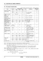
background image


Rev.1.5 


S1F76640 

Technical Manual 


Summary of Contents for S1F76640

Page 1: ...Rev 1 5 S1F76640 Technical Manual ...

Page 2: ...eover no license to any intellectual property rights is granted by implication or otherwise and there is no representation or warranty that anything made in accordance with this material will be free from any patent or copyright infringement of a third party This material or portions thereof may contain technology or the subject relating to strategic products under the control of the Foreign Excha...

Page 3: ...Configuration of product number DEVICES S1 F 76640 M 0C0 000 Packing specifications Specifications Shape M SOP SSOP Model number Model name F Power Supply Product classification S1 Semiconductors ...

Page 4: ......

Page 5: ...2 Pin Functions 4 5 FUNCTIONAL DESCRIPTION 5 6 ELECTRICAL CHARACTERISTICS 8 6 1 Absolute Maximum Ratings 8 6 2 Recommended Operating Conditions 9 6 3 Electrical Characteristics 10 6 4 Measuring Circuit 11 7 CHARACTERISTIC DATA 12 8 APPLIED CIRCUIT EXAMPLES 17 S1F76640 Technical Manual Rev 1 5 EPSON i ...

Page 6: ......

Page 7: ...er supply Therefore it is suitable for supplying micro power to compact electrical devices such as hand held computers with low power consumption 2 FEATURES 1 Highly efficient and low power consuming CMOS DC DC converter 2 Easy conversion from input voltage VDD 3 3V to three types of positive voltages Output 2 VDD 6 6V 3 VDD 9 9V and 4 VDD 13 2V from input VDD 3 3V 3 The use of external parts such...

Page 8: ...3 BLOCK DIAGRAM OSC1 VSS GND OSC2 VDD TC2 TC1 XPOFF RV VREG VOUT CR oscillation circuit Reference voltage generator Voltage stabilizer CAP1 CAP3 CAP2 CAP2 CAP1 Booster Voltage converter VRI Temperature gradient selection circuit Stabilizer Fig 3 1 Block Diagram ...

Page 9: ...echnical Manual Rev 1 5 EPSON 3 4 PIN DESCRIPTION 4 1 Pin Assignment SSOP2 16PIN 1 2 3 4 5 6 7 8 RV VREG TC1 TC2 XPOFF GND VSS OSC1 OSC2 16 15 14 13 12 11 10 9 VRI VOUT CAP3 CAP2 CAP2 CAP1 CAP1 VDD Fig 4 1 SSOP2 16 Pin Assignment ...

Page 10: ...ture gradient selection pin TC2 4 Temperature gradient selection pin VDD 9 Power supply pin Positive side system VCC VOUT 15 Output pin for quadruple boosting VRI 16 Stabilizer input pin VREG 2 Stabilizing voltage output pin RV 1 Stabilizing voltage adjustment pin Adjusts the VREG output voltage by connecting an intermediate tap of the external volume 3 pin resistor connected between the VDD and V...

Page 11: ...nd OSC2 pins and ROSC must be short as much as possible To set the external resistor ROSC first obtain the oscillation frequency fOSC that satisfies the maximum efficiency in Figures 7 12 and 7 13 and then obtain ROSC corresponding to the fOSC in Fig 7 1 The relationship between ROSC and fOSC can be briefly expressed by the following equation on condition that 400kΩ ROSC 2MΩ OSC OSC f 1 A R where ...

Page 12: ...adruple Boosting Voltages Note 1 In triple boosting the double boosting output 10V cannot be extracted from the CAP2 pin Note 2 In quadruple boosting the double boosting output 10V cannot be extracted from the CAP2 pin Note 3 In quadruple boosting the triple boosting output 15V cannot be extracted from the CAP3 pin Reference voltage generator voltage stabilizer The reference voltage generator gene...

Page 13: ...i Z Note 3 OFF 0 VSS H VOUT H VOUT OFF Hi Z ON Boosting only Note 5 Note 1 The high voltage is different between the XPOFF TC2 and TC1 pins Note 2 The temperature gradient CT is defined in the following formula VREG 50 C VREG 0 C 1 CT 100 C 50 C 0 C VREG 25 C Example When CT 0 3 C is selected if VREG output at Ta 25 C is VREG 25 C 8V Δ VREG ΔT CT VREG 25 C 0 3 10 2 8 24mV C is obtained the VREG va...

Page 14: ... VDD 0 3 V CAP2 Output pin voltage 4 V0C4 GND 0 3 4 VDD 0 3 V CAP3 Allowable dissipation Pd 210 mW SSOP 16PIN Operating temperature Topr 40 85 C Storage temperature Tstg 55 150 C Soldering temperature and time Tsol 260 10 C s Lead part Note 1 Use exceeding the absolute maximum ratings above may cause a permanent destruction of the IC A long duration operation at the absolute maximum ratings may si...

Page 15: ...nal resistor for oscillation ROSC 680 2000 kΩ Boosting capacitor C1 C2 C3 C4 3 3 μF Stabilization output adjusting resistor RRV 100 1000 kΩ Note 1 All voltages are based on the condition that the VSS GND is equal to 0V Note 2 For low voltage VDD 1 8 to 2 2V operation the recommended circuit is as follows 1 2 3 4 5 6 7 8 RV VREG TC1 TC2 POFF VSS OSC1 OSC2 16 15 14 13 12 11 10 9 VRI VOUT CAP3 CAP2 C...

Page 16: ...te 3 RSAT 10 Ω RSAT Δ VOUT VREG ΔIOUT 0 IOUT 10mA RV GND Ta 25 C Stabilization output saturated resistance Note 4 Reference voltage VRV0 1 70 1 90 2 20 V TC2 GND TC1 VOUT Ta 25 C VRV1 1 80 2 00 2 20 V TC2 TC1 GND Ta 25 C VRV2 1 50 1 60 1 80 V TC2 VOUT TC1 GND Ta 25 C Temperature CT0 0 40 0 30 0 20 C VDD 5V VOUT 20V gradient CT1 0 50 0 40 0 30 C Note 5 CT2 0 60 0 50 0 40 C Input leak current IL 2 μ...

Page 17: ...6 15 14 13 12 11 10 9 A A V Iopr1 ROSC IO RL C1 C2 C3 C4 VO Stabilization circuit characteristics Measuring circuit 1 2 3 4 5 6 7 8 16 15 14 13 12 11 10 9 A V VO IO R1 R2 VI RL VREG A Iopr2 excluding the current flowing through R1 R2 and RL RRV R1 R2 Input leak current Measuring circuit 1 2 3 4 5 6 7 8 16 15 14 13 12 11 10 9 A Connected to each measurement pin ...

Page 18: ...DD 2V VDD 3V Fig 7 1 Oscillation frequency External resistor for oscillation Fig 7 2 Oscillation frequency 0 10 20 30 40 50 60 70 0 1 2 3 4 5 6 VDD V I OPR1 μ A fOSC 8 75kHz Ta 25 C VDD 5V C1 to C4 10μF fOSC 35kHz fOSC 17 5kHz 0 5 10 15 20 0 10 20 30 IO mA V O V Ta 25 C VDD 5V C1 to C4 10μF Quadruple boosting Triple boosting Double boosting Fig 7 3 Booster current consumption Input voltage Fig 7 4...

Page 19: ...tput current Fig 7 6 Output voltage VO Output current Fig 7 7 Output impedance Input voltage Fig 7 8 Output impedance Input voltage 0 100 200 300 400 500 600 700 0 1 2 3 4 5 6 VDD V R O Ω Ta 25 C IO 5mA Quadruple boosting Triple boosting Double boosting 0 100 200 300 400 500 600 700 0 1 2 3 4 5 6 VDD V R O Ω Ta 25 C IO 10mA Quadruple boosting Triple boosting Double boosting O V Quadruple boosting ...

Page 20: ...IDD Double boosting IDD Fig 7 9 Boosting power conversion efficiency Output current Input current Output current Fig 7 10 Boosting power conversion efficiency Output current Input current Output current 0 10 20 30 40 50 60 70 80 90 100 1 10 100 1000 fOSC kHz Peff Ta 25 C VDD 5V C1 to C4 10μF IO 10mA IO 2mA IO 5mA IO 20mA 0 10 20 30 40 50 60 70 80 90 100 0 1 2 3 4 5 6 7 8 9 10 IO mA Peff 0 10 20 30...

Page 21: ... efficiency Oscillation frequency Fig 7 14 Boosting power conversion efficiency Oscillation frequency Fig 7 15 Boosting start voltage load resistance Fig 7 16 Stabilization output saturated resistance Load current Ta 25 C VDD 3V C1 to C4 10μF IO 5mA IO 2mA IO 10mA IO 1mA 0 0 0 1 0 2 0 3 0 4 0 5 0 5 10 15 20 25 30 IO mA V REG V O V Ta 25 C C1 to C4 10μF VO 20V VO 8V VO 12V 1 6 1 7 1 8 1 9 2 0 2 1 2...

Page 22: ...urrent Fig 7 18 Output voltage VREG Output current 7 85 7 90 7 95 8 00 0 1 1 0 10 0 100 0 IREG mA V REG V Ta 25 C VO 20V 3 85 3 90 3 95 4 00 0 1 1 0 10 0 100 0 IREG mA V 40 30 20 10 0 10 20 30 40 40 20 0 20 40 60 80 100 Ta C V REG Ta V REG 25 C 100 V REG 25 C CT0 CT2 CT1 Fig 7 19 Output voltage VREG Output current Fig 7 20 Reference voltage Temperature REG V Ta 25 C VO 8V ...

Page 23: ...ting Stabilizer Fig 8 3 shows an applied circuit example for stabilizing the boosting output obtained in Fig 8 1 the stabilizer and providing the temperature gradient for the VREG output through the temperature gradient selection circuit This application example can indicate two outputs from VO and VREG at the same time Triple boosting stabilizer operation using the triple boosting and double boos...

Page 24: ...g 8 3 to only one of the n parallel connections shown in Fig 8 5 1 2 3 4 5 6 7 8 9 10 11 12 13 14 15 16 OSC2 OSC1 VSS XPOFF TC2 TC1 VREG RV VRI VO CAP1 CAP1 CAP2 CAP2 CAP3 VDD C4 10μF ROSC 1MΩ C1 10μF C2 10μF C3 10μF VDD R2 R1 VREG RRV 1MΩ 1 2 3 4 5 6 7 8 9 10 11 12 13 14 15 16 OSC2 OSC1 VSS XPOFF TC2 TC1 VREG RV VRI VO CAP1 CAP1 CAP2 CAP2 CAP3 VDD ROSC 1MΩ C1 10μF C2 10μF C3 10μF VSS A VOUT RL IO...

Page 25: ...1 2 3 4 5 6 7 8 9 10 11 12 13 14 15 16 OSC2 OSC1 VSS XPOFF TC2 TC1 VREG RV VRI VO CAP1 CAP1 CAP2 CAP2 CAP3 VDD C4 10μF C1 10μF C2 10μF C3 10μF R2 R1 VREG RRV 1MΩ A C5 10μF 1 2 3 4 5 6 7 8 9 10 11 12 13 14 15 16 OSC2 OSC1 VSS XPOFF TC2 TC1 VREG RV VRI VOUT CAP1 CAP1 CAP2 CAP2 CAP3 VDD ROSC 1MΩ C3 10μF C4 10μF VDD VSS D1 VSS RL IO VOUT VOUT VDD Fig 8 8 Serial Connection Next stage First stage VREG V...

Page 26: ...assigned to triple boosting and the next stage to quadruple boosting however quadruple boosting is available for both the first and next stages unless the input voltage VDD VSS in the next stage exceeds the standard value 6 0V For serial connection each IC must be designed in compliance with the standard VDD VSS 6 0V VO VSS 24V See Fig 8 9 Note 3 When double boosting is provided in the first stage...

Page 27: ...s forward voltage VF of the diode For example as shown in Fig 8 12 VSS 0V VDD 5V and VF 0 6V results in VO 10V 3 0 6V 8 2V 5V 2 0 6V 3 8V for double boosting 10μF 1 2 3 4 5 6 7 8 9 10 11 12 13 14 15 16 OSC2 OSC1 VSS XPOFF TC2 TC1 VREG RV VRI VO CAP1 CAP1 CAP2 CAP2 CAP3 VDD C6 10μF VOUT ROSC 1MΩ VSS VDD 10μF C1 C2 A RL D1 D2 D3 IO VSS 0V VDD 5V VOUT 8 2V 3 VDD 3 VF Fig 8 11 Negative Voltage Convers...

Page 28: ...nversion only 10μF 1 2 3 4 5 6 7 8 9 10 11 12 13 14 15 16 OSC2 OSC1 VSS XPOFF TC2 TC1 VREG RV VRI VOUT CAP1 CAP1 CAP2 CAP2 CAP3 VDD C6 10μF VOUT ROSC 1MΩ VSS VDD 10μF C1 C2 A RL C3 10μF C4 10μF C5 10μF VOUT A RL Io Io Fig 8 14 Negative Voltage Conversion Positive Voltage Conversion VSS 0V VDD 5V VOUT 8 2V 3 VDD 3 VF VOUT 15V 3 VDD Fig 8 15 Diagram of Voltage Relations for Negative Voltage Conversi...

Page 29: ...ne to be changed from Table 5 1 1 2 3 4 5 6 7 8 9 10 11 12 13 14 15 16 OSC2 OSC1 VSS XPOFF TC2 TC1 VREG RV VRI VOUT CAP1 CAP1 CAP2 CAP2 CAP3 VDD C4 10μF VOUT ROSC 1MΩ C1 10μF C2 10μF C3 10μF VDD VREG VSS RT RP Note 2 R2 R1 RRV 1MΩ 10 8 6 4 2 0 2 4 6 8 10 0 10 20 30 40 50 Ta C 100 V REG C V REG 25 C V REG 25 C Thermistor used Thermistor not used Measurement conditions VDD 5V VSS 0V RRV 1MΩ set to V...

Page 30: ...10 9 8 7 6 5 4 3 2 1 VDD CAP1 CAP1 CAP2 Fig 8 20 Electronic Volume Circuit of Voltage Stabilization Output CAP2 CAP3 VOUT VRI RVI VREG VSS OSC1 XPOFF TC2 TC1 OSC2 VSS or VOUT VSS or VOUT 13 14 15 12 1 5 2 4 8 7 16 Negative power input Positive power input 6 CTRL0 CTRL1 CTRL2 Power stabilization output VREG output 3 11 10 9 74HC4051 XPOFF VDD VSS Quadruple boosting IN0 IN1 IN2 IN3 IN4 IN5 IN6 IN7 V...

Page 31: ...ification using two diodes and voltage stabilization output Use the shortest possible wire between VO and VRI Fig 8 22 shows the diagram of voltage relations Use the voltage to be applied to the VRI pin at or below the absolute maximum rated voltage 1 2 3 4 5 6 7 8 9 10 11 12 13 14 15 16 OSC2 OSC1 VSS XPOFF TC2 TC1 VREG RV VRI VO CAP1 CAP1 CAP2 CAP2 CAP3 VDD C4 10μF ROSC 1MΩ C1 10μF C2 10μF C3 10μ...

Page 32: ...r Tower 2 North RD DongSanHuan ChaoYang District Beijing CHINA Phone 86 10 6410 6655 FAX 86 10 6410 7320 SHANGHAI BRANCH 7F High Tech Bldg 900 Yishan Road Shanghai 200233 CHINA Phone 86 21 5423 5522 FAX 86 21 5423 5512 EPSON HONG KONG LTD 20 F Harbour Centre 25 Harbour Road Wanchai Hong Kong Phone 852 2585 4600 FAX 852 2827 4346 Telex 65542 EPSCO HX EPSONElectronic Technology Development Shenzhen ...

Page 33: ...Mouser Electronics Authorized Distributor Click to View Pricing Inventory Delivery Lifecycle Information Epson S1F76640M0C0 ...

Reviews: