MF302-12
S1F70000 Series
T
echnical Manual
IEEE1394 Controller
Technical Manual
S1F70000 Series
EPSON Electronic Devices Website
ELECTRONIC DEVICES MARKETING DIVISION
First issue November,1990 U
Revised July,2001 in Japan H
B
4.5mm
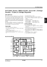
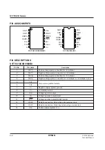
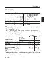
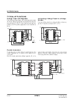
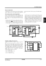
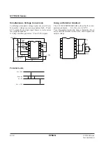
POWER SUPPLY IC
S1F76610 Technical Manual
http://www.epson.co.jp/device/
This manual was made with recycle paper,
and printed using soy-based inks.