background image

Technical Manual

S1C17001

CMOS 16-BIT SINGLE CHIP MICROCONTROLLER

Summary of Contents for S1C17001

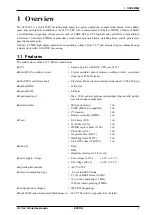
Page 1: ...Technical Manual S1C17001 CMOS 16 BIT SINGLE CHIP MICROCONTROLLER ...

Page 2: ...reover no license to any intellectual property rights is granted by implication or otherwise and there is no representation or warranty that anything made in accordance with this mate rial will be free from any patent or copyright infringement of a third party This material or portions thereof may contain technology or the subject relating to strategic products under the control of the Foreign Exc...

Page 3: ...rcuit Area 3 5 3 4 1 Internal Peripheral Circuit Area 1 0x4000 onward 3 5 3 4 2 Internal Peripheral Circuit Area 2 0x5000 onward 3 5 3 4 3 I O Map 3 6 3 5 Core I O Reserved Area 3 9 4 Power Supply Voltage 4 1 5 Initial Reset 5 1 5 1 Initial Reset Factors 5 1 5 1 1 RESET pin 5 1 5 1 2 P0 Port Key Entry Reset 5 2 5 1 3 Reset by Watchdog Timer 5 2 5 2 Initial Reset Sequence 5 3 5 3 Initial Settings a...

Page 4: ...7 5 8 bit OSC1 Timer Clock Control 7 6 7 6 Clock External Output FOUT3 FOUT1 7 7 7 7 RESET and NMI Input Noise Filters 7 9 7 8 Control Register Details 7 10 0x5060 Clock Source Select Register OSC_SRC 7 11 0x5061 Oscillation Control Register OSC_CTL 7 12 0x5062 Noise Filter Enable Register OSC_NFEN 7 13 0x5064 FOUT Control Register OSC_FOUT 7 14 0x5065 T8OSC1 Clock Control Register OSC_T8OSC1 7 15...

Page 5: ... External Clock Mode 11 3 11 2 3 Pulse Width Measurement Mode 11 4 11 3 Count Mode 11 5 11 4 16 bit Timer Reload Register and Underflow Cycle 11 6 11 5 16 bit Timer Reset 11 7 11 6 16 bit Timer RUN STOP Control 11 8 11 7 16 bit Timer Output Signal 11 9 11 8 16 bit Timer Interrupts 11 10 11 9 Control Register Details 11 11 0x4220 0x4240 0x4260 16 bit Timer Ch x Input Clock Select Registers T16_CLKx...

Page 6: ...Timer 14 4 14 5 Compare Data Settings 14 5 14 6 8 bit OSC1 Timer RUN STOP Control 14 6 14 7 8 bit OSC1 Timer Interrupts 14 7 14 8 Control Register Details 14 9 0x50c0 8 bit OSC1 Timer Control Register T8OSC1_CTL 14 10 0x50c1 8 bit OSC1 Timer Counter Data Register T8OSC1_CNT 14 11 0x50c2 8 bit OSC1 Timer Compare Data Register T8OSC1_CMP 14 12 0x50c3 8 bit OSC1 Timer Interrupt Mask Register T8OSC1_I...

Page 7: ...s 17 7 18 UART 18 1 18 1 UART Configuration 18 1 18 2 UART Pin 18 2 18 3 Transfer Clock 18 3 18 4 Transfer Data Settings 18 4 18 5 Data Transfer Control 18 5 18 6 Receive Errors 18 8 18 7 UART Interrupts 18 9 18 8 IrDA Interface 18 11 18 9 Control Register Details 18 13 0x4100 UART Status Register UART_ST 18 14 0x4101 UART Transmit Data Register UART_TXD 18 16 0x4102 UART Receive Data Register UAR...

Page 8: ...Length Setup Register REMC_CARH 21 13 0x5343 REMC L Carrier Length Setup Register REMC_CARL 21 14 0x5344 REMC Status Register REMC_ST 21 15 0x5345 REMC Length Counter Register REMC_LCNT 21 16 0x5346 REMC Interrupt Mask Register REMC_IMSK 21 17 0x5347 REMC Interrupt Flag Register REMC_IFLG 21 18 21 8 Precautions 21 19 22 On chip Debugger DBG 22 1 22 1 Resource Requirements and Debugging Tool 22 1 2...

Page 9: ...14 0x5040 0x5041 Watchdog Timer AP 15 0x5060 0x5065 Oscillator AP 16 0x5080 0x5081 Clock Generator AP 17 0x50c0 0x50c4 8 bit OSC1 Timer AP 18 0x5200 0x52a3 P Port Port MUX AP 19 0x5300 0x530c PWM Capture Timer AP 21 0x5320 0x5322 MISC Registers AP 22 0x5340 0x5347 Remote Controller AP 23 0xffff80 0xffff90 S1C17 Core I O AP 24 Appendix B Power Saving AP 25 B 1 Clock Control Power Saving AP 25 Appen...

Page 10: ...rnal clock input 32 768 kHz typ s e t y b K 2 3 M O R l a n r e t n I s e t y b K 2 M A R l a n r e t n I l a r e n e g t i b 8 2 x a M t r o p t u p t u o t u p n I purpose input output shared with periph eral circuit input output pins h c 1 e v a l s r e t s a m I P S e c a f r e t n i l a i r e S h c 1 e l b i t a p m o c 0 1 A D r I T R A U I 2C master 1ch h c 1 C M E R r e l l o r t n o c e t...

Page 11: ...ystem 8 16 bits 3 cycles DCLK DST2 DSIO P31 33 REMI P04 REMO P05 P00 07 P10 17 P20 27 P30 33 EXCL0 2 P16 P07 P06 SIN SOUT SCLK P23 25 SDI SDO SPICLK P20 22 8 16 bits 1 cycle I O 2 0x5000 Interrupt controller UART SPI I2C SDA SCL P14 15 I O 1 0x4000 I O port I O MUX TEST0 5 Reset circuit Test circuit RESET Oscillator Clock generator Stopwatch timer PWM capture timer 8 bit OSC1 timer OSC1 2 OSC3 4 F...

Page 12: ...07 EXCL1 A B C D E F G 1 P05 REMO TEST2 P06 EXCL2 P15 SCL P16 EXCL0 LVDD LVDD DSIO P33 DST2 P32 TEST0 P17 SPISS TEST1 P21 SDO VSS VSS VSS VSS VSS P04 REMI DCLK P31 P14 SDA P20 SDI HVDD HVDD P02 P03 P01 P00 P22 SPICLK P23 SIN P24 SOUT P12 P10 P13 FOUT1 P25 SCLK OSC4 P11 RESET P27 EXCL3 TEST4 OSC3 TEST3 P26 TOUT P30 FOUT3 OSC1 OSC2 TEST5 2 3 4 5 6 7 Figure 1 3 1 1 Pinout diagram WCSP 48pin ...

Page 13: ...l Up Input output port pin UART data input pin 24 P22 SPICLK I O I Pull Up Input output port pin SPI clock input output pin 25 P21 SDO I O I Pull Up Input output port pin SPI data output pin 26 P20 SDI I O I Pull Up Input output port pin SPI data input pin 27 P17 SPISS I O I Pull Up Input output port pin with interrupt SPI slave select input pin 28 P16 EXCL0 I O I Pull Up Input output port pin wit...

Page 14: ...ixed 16 bit length Number of commands 111 basic commands 184 in total Execution cycle Main commands executed in one cycle Immediate expansion commands Expansion of immediate to 24 bits Compact high speed command set optimized for development with C Register set 24 bit general purpose register x 8 24 bit special register x 2 8 bit special register x 1 Memory space buses Up to 16 Mbytes of memory sp...

Page 15: ...The S1C17 core contains eight general purpose registers and three special registers R4 R5 R6 R7 R3 R2 R1 R0 PC 7 6 5 4 3 2 1 0 PSR SP IL 2 0 7 6 5 IE 4 C 3 V 2 Z 1 N 0 Bit 23 Bit 0 General purpose registers Bit 23 Bit 0 Special registers Figure 2 2 1 Registers ...

Page 16: ...nsion ld rd rs General purpose register 16 bits General purpose register rd sign7 Immediate General purpose register sign extension rd rb Memory 16 bits General purpose register Memory address post increment post decrement A pre decrement function can be used rd rb rd rb rd rb rd sp imm7 Stack 16 bits General purpose register rd imm7 Memory 16 bits General purpose register rb rs General purpose re...

Page 17: ... sbc rd rs Subtracts 16 bits with carry between general purpose registers Supports conditional execution c Executed when C 1 nc Executed when C 0 sbc c sbc nc sbc rd imm7 Subtracts general purpose register and immediate 16 bits with carry cmp rd rs Compares 16 bits between general purpose registers Supports conditional execution c Executed when C 1 nc Executed when C 0 cmp c cmp nc cmp rd sign7 Co...

Page 18: ...itional PC relative jump Branch conditions Z N V Allows delayed branching jrugt jrugt d sign7 Conditional PC relative jump Branch conditions Z C Allows delayed branching jruge jruge d sign7 Conditional PC relative jump Branch conditions C Allows delayed branching jrult jrult d sign7 Conditional PC relative jump Branch conditions C Allows delayed branching jrule jrule d sign7 Conditional PC relativ...

Page 19: ...general purpose register with address post increment rb Memory specified indirectly by general purpose register with address post decrement rb Memory specified indirectly by general purpose register with address pre decrement sp Stack pointer sp sp imm7 Stack sp Stack with address post increment sp Stack with address post decrement sp Stack with address pre decrement imm3 imm5 imm7 imm13 Immediate...

Page 20: ...ch timer interrupt Timer 100 Hz signal Timer 10 Hz signal Timer 1 Hz signal 7 0x07 0x801c Clock timer interrupt Timer 32 Hz signal Timer 8 Hz signal Timer 2 Hz signal Timer 1 Hz signal 8 0x08 0x8020 8 bit OSC1 timer interrupt Compare match 9 0x09 0x8024 reserved 10 0x0a 0x8028 11 0x0b 0x802c PWM capture timer interrupt Compare A Compare B 12 0x0c 0x8030 8 bit timer interrupt Timer underflow 13 0x0...

Page 21: ...PU core type by the appli cation software 0xffff84 Processor ID Register IDIR Register name Address Bit Name Function Setting Init R W Remarks Processor ID Register IDIR 0xffff84 8 bits D7 0 IDIR 7 0 Processor ID 0x10 S1C17 Core 0x10 0x10 R This is the read only register containing the ID code indicating the processor type The S1C17 core ID code is 0x10 ...

Page 22: ...x425f 0x4220 0x423f 0x4200 0x421f 0x4120 0x41ff 0x4100 0x411f 0x4040 0x40ff 0x4020 0x403f 0x4000 0x401f reserved I2C SPI Interrupt controller reserved 16 bit timer Ch 2 16 bit timer Ch 1 16 bit timer Ch 0 8 bit timer reserved UART reserved Prescaler reserved 0x5360 0x5fff 0x5340 0x535f 0x5320 0x533f 0x5300 0x531f 0x52c0 0x52ff 0x52a0 0x52bf 0x5280 0x529f 0x5200 0x527f 0x50e0 0x51ff 0x50c0 0x50df 0...

Page 23: ...s in the last 24 bits Bus cycle calculation example Number of bus cycles when accessing internal peripheral circuit area 2 8 bit device 3 cycles from CPU using 16 bit read write command 3 cycles x 2 bus accesses 6 CCLK cycles 3 1 1 Access Size Restrictions When programming note that the modules listed below are subject to access size restrictions SPI I2C The SPI and I2C registers can be accessed o...

Page 24: ...to 2 4 Vector Table ROM reads take 1 to 5 cycles 3 2 2 ROM Read Access Cycle Settings Set the IROM area read access cycles using FLCYC 2 0 D 2 0 MISC_FL register to retain compatibility with S1C17701 Normally set FLCYC 2 0 to 0x4 0x5320 ROM Control Register MISC_FL Register name Address Bit Name Function Setting Init R W Remarks ROM Control Register MISC_FL 0x5320 8 bits D7 3 reserved 0 when being...

Page 25: ...n to storing variables it can also be used to copy command codes and execute them rapidly in RAM Note The last 64 bytes of the internal RAM 0x7c0 to 0x7ff are reserved for on chip debugging This area should not be accessed by application programs when using debug functions for exam ple during application development It can be used for applications in mass produced products that do not require debu...

Page 26: ...bit device 8 bit timer T8F 16 bit device 16 bit timer T16 16 bit device Interrupt controller ITC 16 bit device SPI SPI 16 bit device I2C I2C 16 bit device 3 4 2 Internal Peripheral Circuit Area 2 0x5000 onward The internal peripheral circuit area 2 starting at address 0x5000 is assigned for use as the following internal periph eral function I O memory and can be accessed in three cycles Clock time...

Page 27: ..._CTL1 16 bit Timer Ch 1 Control Register Timer mode setting and timer RUN STOP 0x4248 to 0x425f Reserved 16 bit timer Ch 2 16 bit device 0x4260 T16_CLK2 16 bit Timer Ch 2 Input Clock Select Register Prescaler output clock selection 0x4262 T16_TR2 16 bit Timer Ch 2 Reload Data Register Reload data setting 0x4264 T16_TC2 16 bit Timer Ch 2 Counter Data Register Counter data 0x4266 T16_CTL2 16 bit Tim...

Page 28: ... 0x50c5 to 0x50df Reserved P port port MUX 8 bit device 0x5200 P0_IN P0 Port Input Data Register P0 port input data 0x5201 P0_OUT P0 Port Output Data Register P0 port output data 0x5202 P0_IO P0 Port I O Direction Control Register P0 port input output direction selection 0x5203 P0_PU P0 Port Pull up Control Register P0 port pull up control 0x5204 Reserved 0x5205 P0_IMSK P0 Port Interrupt Mask Regi...

Page 29: ...SC register 8 bit device 0x5320 MISC_FL ROM Control Register ROM access condition setting 0x5321 Reserved 0x5322 MISC_OSC1 OSC1 Peripheral Control Register OSC1 operation peripheral function setting for debugging 0x5323 to 0x533f Reserved Remote controller 8 bit device 0x5340 REMC_CFG REMC Configuration Register Transfer selection and permission 0x5341 REMC_PSC REMC Prescaler Clock Select Register...

Page 30: ...Peripheral circuit Address Register name Function S1C17 core I O 0xffff80 TTBR Vector Table Base Register Vector table base address display 0xffff84 IDIR Processor ID Register Processor ID display 0xffff90 DBRAM Debug RAM Base Register Debugging RAM base address display For more information on TTBR refer to 2 4 Vector Table and for more information on IDIR refer to 2 5 Pro cessor Information For m...

Page 31: ...3 MEMORY MAP AND BUS CONTROL 22 EPSON S1C17001 TECHNICAL MANUAL This page intentionally left blank ...

Page 32: ...oltages are given below Core voltage LVDD 1 65 V to 2 7 V I O voltage HVDD 1 65 V to 3 6 V Supply voltages within the respective ranges to LVDD and HVDD pins with the VSS pin as GND The S1C17001 has two LVDD pins two HVDD pins and five VSS pins All must be connected to the power supply and GND None should be left open ...

Page 33: ...4 POWER SUPPLY VOLTAGE 24 EPSON S1C17001 TECHNICAL MANUAL This page intentionally left blank ...

Page 34: ...n standby circuit Figure 5 1 1 Initial reset circuit configuration The CPU and peripheral circuits are initialized by initial reset factors The CPU begins reset processing once the factors are canceled This causes the reset vector to be read from the start of the vector table and the program initialization routine starting at that address to be executed 5 1 1 RESET pin Initial resetting is possibl...

Page 35: ...ey entry reset function The P0 port key entry reset function is enabled by software and cannot be used to perform a reset at power on The P0 port key entry reset function cannot be used in SLEEP state 5 1 3 Reset by Watchdog Timer The S1C17001 incorporates a watchdog timer to detect runaway CPU If the watchdog timer is not reset by soft ware every 4 seconds with this failure indicating a runaway C...

Page 36: ...sync with the OSC3 clock after the reset is canceled fosc3 OSC3 clock frequency Note The oscillation stabilization standby time does not include the oscillation start time The time may be longer than that shown between power on or SLEEP cancellation and command ex ecution Boot vector Oscillation stabilization standby time Boot operation start OSC3 clock RESET Reset cancellation Internal data reque...

Page 37: ...r table is loaded by reset processing The internal RAM and display memory should be initialized via software since they are not initialized by initial resetting The internal peripheral circuits are initialized in accordance with their particular specifications They should be reset via software if necessary For detailed information on initial values after initial resetting refer to the I O register...

Page 38: ...er when multiple interrupts occur simultaneously can be set separately for each interrupt circuit Each interrupt circuit includes the number of interrupt factors indicated in parentheses above The respective pe ripheral module register controls the specific interrupt factor used to generate the interrupt request to the ITC For detailed information on interrupt factors and interrupt factor control ...

Page 39: ... 6 0x06 0x8018 Stopwatch timer interrupt Timer 100 Hz signal Timer 10 Hz signal Timer 1 Hz signal 7 0x07 0x801c Clock timer interrupt Timer 32 Hz signal Timer 8 Hz signal Timer 2 Hz signal Timer 1 Hz signal 8 0x08 0x8020 8 bit OSC1 timer interrupt Compare match 9 0x09 0x8024 reserved 10 0x0a 0x8028 11 0x0b 0x802c PWM capture timer interrupt Compare A Compare B 12 0x0c 0x8030 8 bit timer interrupt ...

Page 40: ...ster 13 16 bit timer Ch 0 interrupt Timer underflow IIFT1 D9 ITC_IFLG register 14 16 bit timer Ch 1 interrupt Timer underflow IIFT2 D10 ITC_IFLG register 15 16 bit timer Ch 2 interrupt Timer underflow IIFT3 D11 ITC_IFLG register 16 UART interrupt Transmit buffer empty Receive buffer full Receive error IIFT4 D12 ITC_IFLG register 17 Remote controller interrupt Data length counter underflow Input ri...

Page 41: ...ister 8 8 bit OSC1 timer interrupt EIFT4 D4 ITC_IFLG register EIEN4 D4 ITC_EN register 11 PWM capture timer interrupt EIFT7 D7 ITC_IFLG register EIEN7 D7 ITC_EN register 12 8 bit timer interrupt IIFT0 D8 ITC_IFLG register IIEN0 D8 ITC_EN register 13 16 bit timer Ch 0 interrupt IIFT1 D9 ITC_IFLG register IIEN1 D9 ITC_EN register 14 16 bit timer Ch 1 interrupt IIFT2 D10 ITC_IFLG register IIEN2 D10 I...

Page 42: ... interrupt IILV6 2 0 D 2 0 ITC_ILV3 register 0x4314 19 I2C interrupt IILV7 2 0 D 10 8 ITC_ILV3 register 0x4314 The interrupt level can range from 0 to 7 The interrupt level set is issued to the S1C17 core at the same time as an interrupt request from the ITC This inter rupt level is used in the S1C17 core to prohibit subsequent interrupts with the same or lower levels refer to Section 6 3 6 Initia...

Page 43: ...D4 ITC_ELV2 register 0x430a PWM capture timer interrupt EITG7 D12 ITC_ELV3 register 0x430c The module setting the IIFT flag outputs a pulse signal only as the interrupt request to the ITC No trigger mode selector bit is provided Pulse trigger mode In pulse trigger mode the ITC samples the interrupt signal using the system clock rising edge If a pulse High period is detected the ITC sets the interr...

Page 44: ...d by the S1C17 core and the interrupt signal must subsequently be cleared pclk Interrupt signal set to inactive by interrupt source Interrupt signal from interrupt source Interrupt flag within ITC Figure 6 3 5 2 Level trigger mode Note The S1C17001 interrupts listed below are in level trigger mode The interrupt flag within pe ripheral modules must be reset to 1 within the interrupt processing rout...

Page 45: ...th the highest level becomes the subject of the interrupt request to the S1C17 core Interrupts with lower levels are held until the above conditions are subsequently met The S1C17 core samples interrupt requests for each cycle On accepting an interrupt request the S1C17 core switches to interrupt processing when execution of the current command is complete Interrupt processing involves the followi...

Page 46: ...s using the watchdog timer The vector number for NMIs is 2 and the vector address is set in the vector table initial address 8 bytes These interrupts take prece dence over other interrupt factors and are accepted unconditionally by the S1C17 core For detailed information on generating NMIs refer to 17 Watchdog Timer WDT ...

Page 47: ...core int imm5 or intl imm5 and imm3 commands The vector table vector number 0 to 31 is specified by the operand immediate imm5 With the intl command imm3 can be used to specify an interrupt level 0 to 7 for the PSR IL fields Details of the processor interrupt processing are the same as for when an interrupt generated by hardware occurs ...

Page 48: ...e canceled by interrupt factors and the CPU starts up The interrupt factors capable of starting the CPU and specific program execution details after CPU startup whether to branch into an interrupt processing routine depend on the clock states in HALT and SLEEP modes For more information refer to B 1 Clock Control Power Saving in Appendix B ...

Page 49: ...TC_ELV2 External Interrupt Level Setup Register 2 Sets 8 bit OSC1 timer interrupt level and trigger mode 0x430c ITC_ELV3 External Interrupt Level Setup Register 3 Sets PWM capture timer interrupt level and trigger mode 0x430e ITC_ILV0 Internal Interrupt Level Setup Register 0 Sets 8 bit timer and 16 bit timer Ch 0 interrupt level 0x4310 ITC_ILV1 Internal Interrupt Level Setup Register 1 Sets 16 bi...

Page 50: ...lt 1 W Reset flag 0 W Disabled The interrupt flags are reset to 1 if an interrupt factor occurs in the peripheral modules An interrupt is generated to the S1C17 core provided the following conditions are met 1 The corresponding interrupt enable bit is set to 1 2 No other interrupt having requests higher priority levels have occurred 3 The PSR IE bit was set to 1 interrupt permitted 4 The correspon...

Page 51: ...terrupt flag Hardware interrupt factor EIFT0 D0 P0 port interrupt P00 to P07 port input EIFT1 D1 P1 port interrupt P10 to P17 port input EIFT2 D2 Stopwatch timer interrupt 100 Hz 10 Hz 1 Hz signal EIFT3 D3 Clock timer interrupt 32 Hz 8 Hz 2 Hz 1 Hz signal EIFT4 D4 8 bit OSC1 timer interrupt Compare match EIFT7 D7 PWM capture timer interrupt Compare A Compare B match Note The interrupt flags are no...

Page 52: ...rupt permitted 0 R W Interrupt prohibited default Setting the interrupt enable bit to 1 permits interrupts Setting it to 0 prohibits interrupts Even if interrupt prohibition has been set the corresponding interrupt can still be used to cancel Stand by mode Table 6 7 4 Hardware interrupt factors and interrupt enable bits Interrupt enable bit Hardware interrupt factor EIEN0 D0 P0 port interrupt P00 ...

Page 53: ...ss Bit Name Function Setting Init R W Remarks ITC Control Register ITC_CTL 0x4304 16 bits D15 1 reserved 0 when being read D0 ITEN ITC enable 1 Enable 0 Disable 0 R W D 15 1 Reserved D0 ITEN ITC Enable Bit Permits interrupt control using the ITC 1 R W Permitted 0 R W Prohibited default Set to 1 before using the ITC ...

Page 54: ...t by writing 1 in this mode The interrupt signal must be maintained at High until the interrupt source module is accepted by the S1C17 core and the interrupt signal must then be cleared D11 Reserved D 10 8 EILV1 2 0 P1 Port Interrupt Level Bits Set the P1 port interrupt level 0 to 7 Default 0 The S1C17 core does not accept interrupts with levels set lower than the PSR IL value The ITC uses the int...

Page 55: ...t Trigger Mode Select Bit Selects clock timer interrupt trigger mode This should be set to 1 for the S1C17001 1 R W Level trigger mode 0 R W Pulse trigger mode default Refer to the ITC_ELV0 register 0x4306 EITG1 D12 description D11 Reserved D 10 8 EILV3 2 0 Clock Timer Interrupt Level Bits Set the clock timer interrupt level 0 to 7 Default 0 Refer to the ITC_ELV0 register 0x4306 EILV1 2 0 D 10 8 d...

Page 56: ...o 1 D3 reserved 0 when being read D2 0 EILV4 2 0 T8OSC1 interrupt level 0 to 7 0x0 R W D 15 5 Reserved D4 EITG4 8 bit OSC1 Timer Interrupt Trigger Mode Select Bit Selects 8 bit OSC1 timer interrupt trigger mode This should be set to 1 for the S1C17001 1 R W Level trigger mode 0 R W Pulse trigger mode default Refer to the ITC_ELV0 register 0x4306 EITG1 D12 description D3 Reserved D 2 0 EILV4 2 0 8 ...

Page 57: ...g read D10 8 EILV7 2 0 T16E interrupt level 0 to 7 0x0 R W D7 0 reserved 0 when being read D 15 13 Reserved D12 EITG7 PWM Capture Timer Interrupt Trigger Mode Select Bit Selects PWM capture timer interrupt trigger mode This should be set to 1 for the S1C17001 1 R W Level trigger mode 0 R W Pulse trigger mode default Refer to the ITC_ELV0 register 0x4306 EITG1 D12 description D11 Reserved D 10 8 EI...

Page 58: ...le interrupts occur at the same time permi tted by the interrupt enable bit the ITC sends the in terrupt request with the highest level set by the ITC_ELVx and ITC_ILVx registers 0x4306 to 0x4314 to the S1C17 core If multiple interrupt factors with the same interrupt level occur simultaneously the interrupt with the lowest vector number is processed first The other interrupts are held until all ha...

Page 59: ...terrupt level 0 to 7 0x0 R W D7 3 reserved 0 when being read D2 0 IILV2 2 0 T16 Ch 1 interrupt level 0 to 7 0x0 R W D 15 11 Reserved D 10 8 IILV3 2 0 16 bit Timer Ch 2 Interrupt Level Bits Set the 16 bit timer Ch 2 interrupt level 0 to 7 Default 0 Refer to the ITC_ILV0 register 0x430e IILV1 2 0 D 10 8 description D 7 3 Reserved D 2 0 IILV2 2 0 16 bit Timer Ch 1 Interrupt Level Bits Set the 16 bit ...

Page 60: ...5 2 0 REMC interrupt level 0 to 7 0x0 R W D7 3 reserved 0 when being read D2 0 IILV4 2 0 UART interrupt level 0 to 7 0x0 R W D 15 11 Reserved D 10 8 IILV5 2 0 Remote Controller Interrupt Level Bits Set the remote controller interrupt level 0 to 7 Default 0 Refer to the ITC_ILV0 register 0x430e IILV1 2 0 D 10 8 description D 7 3 Reserved D 2 0 IILV4 2 0 UART Interrupt Level Bits Set the UART interr...

Page 61: ... read D10 8 IILV7 2 0 I2C interrupt level 0 to 7 0x0 R W D7 3 reserved 0 when being read D2 0 IILV6 2 0 SPI interrupt level 0 to 7 0x0 R W D 15 11 Reserved D 10 8 IILV7 2 0 I2C Interrupt Level Bits Set the I2C interrupt level 0 to 7 Default 0 Refer to the ITC_ILV0 register 0x430e IILV1 2 0 D 10 8 description D 7 3 Reserved D 2 0 IILV6 2 0 SPI Interrupt Level Bits Set the SPI interrupt level 0 to 7...

Page 62: ...are in level trigger mode P0 port interrupt P1 port interrupt Stopwatch timer interrupt Clock timer interrupt 8 bit OSC1 timer interrupt PWM capture timer interrupt Make sure all EITGx bits within the ITC_ELVx registers 0x4306 to 0x430c have been set to 1 level trigger mode The interrupt flag within peripheral modules must be reset to 1 within the interrupt processing routine rather than EIFTx For...

Page 63: ...6 INITERRUPT CONTROLLER 54 EPSON S1C17001 TECHNICAL MANUAL This page intentionally left blank ...

Page 64: ...OSC1 oscillator circuit 32 768 kHz Division circuit 1 1 to 1 4 Wait circuit for wakeup Clock gear 1 1 to 1 8 Gate S1C17 core BCLK Internal bus RAM ROM ITC T16 T8F UART SPI I2C T16E P MISC REMC Control register CT SWT WDT T8OSC1 PCLK CLK_256Hz OSC3 OSC4 Clock source selection System clock FOUT3 FOUT1 output circuit FOUT1 Noise filter RESET OSC1 OSC2 SLEEP on off control Gear selection wakeup HALT O...

Page 65: ...tor X tal3 or ceramic oscillator Ceramic and feedback resistor Rf should be connected between the OSC3 and OSC4 pins Two capacitors CG3 and CD3 should also be connected between the OSC3 OSC4 pins and VSS A drain resistor Rd should be connected between the OSC4 pin and CD3 if required When used with external clock input the OSC4 pin should be left free and a clock with a duty ratio of 50 at LVDD le...

Page 66: ...n be selected using the OSC3WT 1 0 D 5 4 OSC_CTL register OSC3WT 1 0 OSC3 Wait Cycle Select Bits in the Oscillation Control OSC_CTL Register D 5 4 0x5061 Table 7 2 2 OSC3 oscillation stabilization wait time settings OSC3WT 1 0 Oscillation stabilization wait time 0x3 128 cycles 0x2 256 cycles 0x1 512 cycles 0x0 1 024 cycles Default 0x0 This is set to 1 024 cycles OSC3 clock after initial resetting ...

Page 67: ...tal1 typ 32 768 kHz and feedback resistor Rf between the OSC1 and OSC2 pins Connect two capacitors CG1 and CD1 between the OSC1 OSC2 pins and VSS A drain resistor Rd should be connected between the OSC2 pin and CD1 if required When used with external clock max 100 kHz input the OSC2 pin should be left free and a clock with a duty ra tio of 50 at LVDD level should be input to the OSC1 pin If the OS...

Page 68: ...ock 256 cycle pe riod OSC3 oscillation cannot be stopped before switching the system clock to OSC1 OSC1 to OSC3 1 Set the OSC3WT 1 0 D 5 4 OSC_CTL register to an oscillation stabilization wait time see Table 7 2 2 at least as long as OSC3 oscillation start time Not necessary if already set OSC3WT 1 0 OSC3 Wait Cycle Select Bits in the Oscillation Control OSC_CTL Register D 5 4 0x5061 2 If the OSC3...

Page 69: ...ock division ratio using T8O1CK 2 0 D 3 1 OSC_T8OSC1 register T8O1CK 2 0 T8OSC1 Clock Division Ratio Select Bits in the T8OSC1 Clock Control OSC_T8OSC1 Register D 3 1 0x5065 Table 7 5 1 T8OSC1 clock division ratio selection T8O1CK 2 0 Division ratio 0x7 to 0x6 Reserved 0x5 OSC1 1 32 0x4 OSC1 1 16 0x3 OSC1 1 8 0x2 OSC1 1 4 0x1 OSC1 1 2 0x0 OSC1 1 1 Default 0x0 Clock feed control The clock feed to t...

Page 70: ...X P30 Port Function Select Bit in the P3 Port Function Select P3_PMUX Register D0 0x52a3 FOUT3 clock frequency selection Three different clock output frequencies can be selected Select the division ratio for the OSC3 clock using FOUT3D 1 0 D 3 2 OSC_FOUT register FOUT3D 1 0 FOUT3 Clock Division Ratio Select Bits in the FOUT Control OSC_FOUT Register D 3 2 0x5064 Table 7 6 1 FOUT3 clock division ra...

Page 71: ...P13MUX P13 Port Function Select Bit in the P1 Port Function Select P1_PMUX Register D3 0x52a1 Clock output control The clock output is controlled using the FOUT1E D0 OSC_FOUT register Setting FOUT1E to 1 outputs the FOUT1 clock from the FOUT1 pin Setting it to 0 halts output FOUT1E FOUT1 Output Enable Bit in the FOUT Control OSC_FOUT Register D1 0x5064 FOUT1E FOUT1 output P13 0 0 1 Figure 7 6 3 FO...

Page 72: ...ise when RSTFE D1 OSC_NFEN register 1 bypassed when RSTFE 0 NMI input noise filter Filters noise when NMIFE D0 OSC_NFEN register 1 bypassed when NMIFE 0 RSTFE Reset Noise Filter Enable Bit in the Noise Filter Enable OSC_NFEN Register D1 0x5062 NMIFE NMI Noise Filter Enable Bit in the Noise Filter Enable OSC_NFEN Register D0 0x5062 The noise filters operate using the system clock OSC3 or OSC1 clock...

Page 73: ...illation Control Register Oscillation control 0x5062 OSC_NFEN Noise Filter Enable Register Noise filter on off 0x5064 OSC_FOUT FOUT Control Register Clock external output control 0x5065 OSC_T8OSC1 T8OSC1 Clock Control Register 8 bit OSC1 timer clock setting The OSC module registers are described in detail below These are 8 bit registers Note When data is written to the registers the Reserved bits ...

Page 74: ...SC1 0 OSC3 0 R W D 7 1 Reserved D0 CLKSRC System Clock Source Select Bit Selects the system clock source 1 R W OSC1 0 R W OSC3 default OSC3 is selected for normal high speed operations If the OSC3 clock is not required OSC1 can be set as the system clock and OSC3 stopped to reduce power consumption Note If the system clock is switched from OSC3 to OSC1 immediately after starting OSC1 oscilla tion ...

Page 75: ...n wait time settings OSC3WT 1 0 Oscillation stabilization wait time 0x3 128 cycles 0x2 256 cycles 0x1 512 cycles 0x0 1 024 cycles Default 0x0 This is set to 1 024 cycles OSC3 clock after initial resetting The CPU does not begin operating im mediately after resetting until this time has elapsed Note The OSC3 oscillation start time depends on the oscillator and externally connected compo nents The t...

Page 76: ... noise filter inputs only RESET pulses of not less than 16 cycles of the system clock OSC3 or OSC1 clock to the S1C17 core Pulses having widths of less than 16 cycles are filtered out as noise This should normally be enabled D0 NMIFE NMI Noise Filter Enable Bit Enables or disables the NMI input noise filter 1 R W Enabled noise filtering default 0 R W Disabled bypass This noise filter inputs only N...

Page 77: ... OSC3 division clock external output 1 R W Permitted on 0 R W Prohibited off default Setting FOUT3E to 1 outputs the FOUT3 clock from the FOUT3 pin Setting it to 0 stops the output The FOUT3 output pin is combined with the P30 port This functions as the P30 port pin by default so the pin function should be changed by writing 1 to P30MUX D0 P3_PMUX register if use is required for FOUT3 output P30MU...

Page 78: ...rved D 3 1 T8O1CK 2 0 T8OSC1 Clock Division Ratio Select Bits Select the OSC1 clock division ratio and set the 8 bit OSC1 timer operation clock Table 7 8 4 T8OSC1 clock division ratio selection T8O1CK 2 0 Division ratio 0x7 to 0x6 Reserved 0x5 OSC1 1 32 0x4 OSC1 1 16 0x3 OSC1 1 8 0x2 OSC1 1 4 0x1 OSC1 1 2 0x0 OSC1 1 1 Default 0x0 D0 T8O1CE T8OSC1 Clock Output Enable Bit Permits or prohibits clock ...

Page 79: ...Characteristics Switching the system clock from OSC3 to OSC1 immediately after starting OSC1 oscillation will stop the sys tem clock until the OSC1 clock starts up for the OSC1 clock 256 cycle period The OSC3 oscillator circuit cannot be stopped if the OSC3 clock is being used as the system clock The OSC1 oscillator circuit cannot be stopped if the OSC1 clock is being used as the system clock Sinc...

Page 80: ...3 OSC4 FOUT3 FOUT1 output circuit FOUT1 Noise filter RESET OSC1 OSC2 SLEEP on off control Gear selection wakeup HALT On off control S1C17 core S1C17 core Division ratio selection On off control On off control On off control SLEEP on off control Noise filter NMI On off control Division circuit CT SWT WDT T8OSC1 Gate Gate On off control On off control Gate CLG PSC OSC T8F T16 T16E REMC P UART SPI I2...

Page 81: ...io to reduce system clock speeds CCLKGR 1 0 CCLK Clock Gear Ratio Select Bits in the CCLK Control CLG_CCLK Register D 1 0 0x5081 Table 8 2 1 CCLK gear ratio selection CCLKGR 1 0 Gear ratio 0x3 1 8 0x2 1 4 0x1 1 2 0x0 1 1 Default 0x0 Clock feed control The CCLK clock feed is stopped by executing the halt command Since this does not stop the system clock pe ripheral modules will continue to operate ...

Page 82: ...CLG_PCLK register PCKEN 1 0 PCLK Enable Bits in the PCLK Control CLG_PCLK Register D 1 0 0x5080 Table 8 3 1 PCLK control PCKEN 1 0 PCLK feed 0x3 Permitted on 0x2 Setting prohibited 0x1 Setting prohibited 0x0 Prohibited off Default 0x3 The default setting is 0x3 which enables the clock feed Stop the clock feed to reduce power consumption un less all peripheral modules modules listed above within th...

Page 83: ... Register name Function 0x5080 CLG_PCLK PCLK Control Register PCLK feed control 0x5081 CLG_CCLK CCLK Control Register CCLK division ratio setting The CLG module registers are described in detail below These are 8 bit registers Note When data is written to the registers the Reserved bits must always be written as 0 and not 1 ...

Page 84: ... 0x0 Prohibited off Default 0x3 The PCKEN 1 0 default setting is 0x3 which enables clock feed Stop the clock feed to reduce power consumption if the peripheral modules listed below are not required Peripheral modules operated using PCLK Prescaler PWM capture timer remote controller P port UART 8 bit timer 16 bit timer Ch 0 to 2 Interrupt controller SPI I2C P port port MUX PWM capture timer MISC re...

Page 85: ...K clock gear ratio select CCLKGR 1 0 Gear ratio 0x0 R W 0x3 0x2 0x1 0x0 1 8 1 4 1 2 1 1 D 7 2 Reserved D 1 0 CCLKGR 1 0 CCLK Clock Gear Ratio Select Bits Select the gear ratio for reducing system clock speed and set the CCLK clock speed for operating the S1C17 core To reduce power consumption operate the S1C17 core using the slowest possible clock speed Table 8 4 3 CCLK gear ratio selection CCLKGR...

Page 86: ...mer Ch 0 to 2 Interrupt controller SPI I2C P port port MUX PWM capture timer MISC register Remote controller Since the following peripheral modules are not operated using PCLK except for control register access PCLK is not required after setting the control register to start operations Clock timer Stopwatch timer Watchdog timer 8 bit OSC1 timer 2 Do not set PCKEN 1 0 D 1 0 CLG_PCLK register to 0x2...

Page 87: ...8 CLOCK GENERATOR CLG 78 EPSON S1C17001 TECHNICAL MANUAL This page intentionally left blank ...

Page 88: ...controlled by the PRUN bit D0 PSC_CTL register To operate the prescaler write 1 to PRUN Writing 0 to PRUN stops the prescaler Stopping the prescaler while the timer and interface module are halted en ables the current consumption to be reduced The prescaler is stopped immediately after initial resetting PRUN Prescaler Run Stop Control Bit in the Prescaler Control PSC_CTL Register D0 0x4020 Note PC...

Page 89: ...escaler run stop in debug mode 1 Run 0 Stop 0 R W D0 PRUN Prescaler run stop control 1 Run 0 Stop 0 R W D 7 2 Reserved D1 PRUND Prescaler Run Stop Setting Bit for Debug Mode Selects prescaler operations in Debug mode 1 R W Operate 0 R W Stop default Setting PRUND to 1 operates the prescaler even in Debug mode Setting it to 0 stops the prescaler once the S1C17 core switches to Debug mode Set PRUND ...

Page 90: ...9 PRESCALER PSC S1C17001 TECHNICAL MANUAL EPSON 81 9 3 Precautions PCLK must be fed from the clock generator to use the prescaler ...

Page 91: ...9 PRESCALER PSC 82 EPSON S1C17001 TECHNICAL MANUAL This page intentionally left blank ...

Page 92: ... port configuration HVDD VSS Internal data bus Pxy Peripheral module input Peripheral module output Peripheral module I O control PxPUy PxIOy PxOUTy PxyMUX Pull up enable Input output direction selection Output data Function selection Figure 10 1 1 Input output port configuration The P0 and P1 ports can generate input interrupts The P0 3 0 port can be used for key entry resets For more information...

Page 93: ...0 T16CH0 P17 SPISS SPI P17MUX D7 P1 Port Function Select P1_PMUX Register 0x52a1 P20 SDI SPI P20MUX D0 P2 Port Function Select P2_PMUX Register 0x52a2 P21 SDO SPI P21MUX D1 P22 SPICLK SPI P22MUX D2 P23 SIN UART P23MUX D3 P24 SOUT UART P24MUX D4 P25 SCLK UART P25MUX D5 P26 TOUT T16E P26MUX D6 P27 EXCL3 T16E P27MUX D7 P30 FOUT3 OSC P30MUX D0 P3 Port Function Select P3_PMUX Register 0x52a3 DCLK DBG P...

Page 94: ...N 7 0 Px_IN register The value read will be 1 when the input pin is at High HVDD level and 0 when it is at Low VSS level P0IN 7 0 P0 7 0 Port Input Data Bits in the P0 Port Input Data P0_IN Register D 7 0 0x5200 P1IN 7 0 P1 7 0 Port Input Data Bits in the P1 Port Input Data P1_IN Register D 7 0 0x5210 P2IN 7 0 P2 7 0 Port Input Data Bits in the P2 Port Input Data P2_IN Register D 7 0 0x5220 P3IN 3...

Page 95: ...ables the pull up resistor and pulls up the port pin in input mode It will not be pulled up if set to 0 The PxPU 7 0 setting is disabled in output mode and the pin is not pulled up Input output ports that are not used should be set with pull up enabled This pull up setting is also enabled for ports for which the peripheral module function has been selected A delay will occur in the waveform rise u...

Page 96: ...10 INPUT OUTPUT PORT P S1C17001 TECHNICAL MANUAL EPSON 87 10 5 Input Interface Level The S1C17001 input interface level is pegged to the CMOS mute level ...

Page 97: ...rification time Off Default 0x0 when OSC3 2 MHz and PCLK OSC3 Note The chattering filter verification time refers to the maximum pulse width that can be filtered Generating an input interrupt requires a minimum input time of the verification time and a maximum input time of twice the verification time Input interrupts will not be accepted for a transition into SLEEP mode with the chattering filter...

Page 98: ... in the P0 Port Interrupt Mask P0_IMSK Register D 7 0 0x5205 P1IE 7 0 P1 7 0 Port Interrupt Enable Bits in the P1 Port Interrupt Mask P1_IMSK Register D 7 0 0x5215 Setting PxIE 7 0 to 1 enables interrupt generation by the corresponding port Setting to 0 default disables in terrupt generation The interrupt controller must also be set to actually generate an interrupt For more information on making ...

Page 99: ...errupts are permitted as previously set detects the specified edge of an input signal The interrupt level and interrupt permission should be set for the ITC register in order to generate a port inter rupt Table 10 7 1 illustrates the port interrupt ITC control bits Table 10 7 1 ITC control bits Port Interrupt flag Interrupt enable Interrupt level setting Trigger mode setting P0 EIFT0 D0 ITC_IFLG E...

Page 100: ...C17001 TECHNICAL MANUAL EPSON 91 Interrupt vector The port interrupt vector numbers and vector addresses are as shown below Table 10 7 2 Port interrupt vectors Port Vector number Vector address P0 4 0x04 0x8010 P1 5 0x05 0x8014 ...

Page 101: ...rol Register P1 port pull up control 0x5215 P1_IMSK P1 Port Interrupt Mask Register P1 port interrupt mask setting 0x5216 P1_EDGE P1 Port Interrupt Edge Select Register P1 port interrupt edge selection 0x5217 P1_IFLG P1 Port Interrupt Flag Register P1 port interrupt occurrence status display reset 0x5220 P2_IN P2 Port Input Data Register P2 port input data 0x5221 P2_OUT P2 Port Output Data Registe...

Page 102: ...7 0 P2IN 7 0 P2 7 0 port input data 1 1 H 0 0 L R P3 Port Input Data Register P3_IN 0x5230 8 bits D7 4 reserved 0 when being read D3 0 P3IN 3 0 P3 3 0 port input data 1 1 H 0 0 L R Note The x in the bit names indicates the port number 0 to 3 D 7 0 PxIN 7 0 Px 7 0 Port Input Data Bits P3 port is P3IN 3 0 Read out the P port pin status Default external pin status 1 R High level 0 R Low level PxIN 7 ...

Page 103: ...x5221 8 bits D7 0 P2OUT 7 0 P2 7 0 port output data 1 1 H 0 0 L 0 R W P3 Port Output Data Register P3_OUT 0x5231 8 bits D7 4 reserved 0 when being read D3 0 P3OUT 3 0 P3 3 0 port output data 1 1 H 0 0 L 0 R W Note The x in the bit names indicates the port number 0 to 3 D 7 0 PxOUT 7 0 Px 7 0 Port Output Data Bits P3 port is P3OUT 3 0 Set the data to be output from the port pin 1 R W High level 0 R...

Page 104: ...P2 7 0 port I O direction select 1 Output 0 Input 0 R W P3 Port I O Direction Control Register P3_IO 0x5232 8 bits D7 4 reserved 0 when being read D3 0 P3IO 3 0 P3 3 0 port I O direction select 1 Output 0 Input 0 R W Note The x in the bit names indicates the port number 0 to 3 D 7 0 PxIO 7 0 Px 7 0 Port I O Direction Select Bits P3 port is P3IN 3 0 Set the input output mode for the input output po...

Page 105: ...e or disable the pull up resistor included in each port 1 R W Enabled default 0 R W Disabled PxPU 7 0 are the pull up control bits that correspond directly to the Px 7 0 ports Setting to 1 enables the pull up resistor and pulls up the port pin in input mode It will not be pulled up if set to 0 The PxPU 7 0 setting is disabled in output mode and the pin is not pulled up Input output ports that are ...

Page 106: ... 0 port interrupt enable 1 Enable 0 Disable 0 R W Note The x in the bit names indicates the port number 0 or 1 D 7 0 PxIE 7 0 Px 7 0 Port Interrupt Enable Bits Permit or prohibit P0 7 0 and P1 7 0 port interrupt 1 R W Interrupt permitted 0 R W Interrupt prohibited default Setting PxIE 7 0 to 1 permits the corresponding interrupt while setting to 0 blocks interrupts Status changes for the input pin...

Page 107: ...dge 0 R W P1 Port Interrupt Edge Select Register P1_EDGE 0x5216 8 bits D7 0 P1EDGE 7 0 P1 7 0 port interrupt edge select 1 Falling edge 0 Rising edge 0 R W Note The x in the bit names indicates the port number 0 or 1 D 7 0 PxEDGE 7 0 Px 7 0 Port Interrupt Edge Select Bits Select the input signal edge for generating P0 7 0 and P1 7 0 port interrupts 1 R W Falling edge 0 R W Rising edge default Port...

Page 108: ...e corresponding PxIE 7 0 Px_IMSK register to 1 sets PxIF 7 0 to 1 at the specified edge rising or falling edge of the input signal A P0 or P1 port interrupt request signal is also output to the ITC at the same time This interrupt request signal causes the P0 P1 port interrupt flag inside the ITC to be set to 1 Meeting the ITC and S1C17 core interrupt conditions generates an interrupt The following...

Page 109: ... if used individually for the four P0 3 0 and P0 7 4 ports using P0CFx 2 0 Table 10 8 2 Chattering filter function settings P0CFx 2 0 Verification time 0x7 16384 fPCLK 8ms 0x6 8192 fPCLK 4ms 0x5 4096 fPCLK 2ms 0x4 2048 fPCLK 1ms 0x3 1024 fPCLK 512μs 0x2 512 fPCLK 256μs 0x1 256 fPCLK 128μs 0x0 No verification time Off Default 0x0 when OSC3 2 MHz and PCLK OSC3 Note The chattering filter verification...

Page 110: ... key entry input reset settings P0KRST 1 0 Ports used 0x3 P00 P01 P02 P03 0x2 P00 P01 P02 0x1 P00 P01 0x0 Not used Default 0x0 The key entry reset function performs an initial reset by inputting Low level simultaneously from exter nally to the port selected here For example if P0KRST 1 0 is set to 0x3 an initial reset is performed when the four ports P00 to P03 are simultaneously set to Low level ...

Page 111: ...5 P05MUX P05 port function select 1 REMO 0 P05 0 R W D4 P04MUX P04 port function select 1 REMI 0 P04 0 R W D3 0 reserved 0 when being read The P04 and P05 input output port pins are shared with the peripheral module pins This register is used to select how the pins are used D 7 6 Reserved D5 P05MUX P05 Port Function Select Bit 1 R W REMO REMC 0 R W P05 port default D4 P04MUX P04 Port Function Sele...

Page 112: ...on select 1 SDA 0 P14 0 R W D3 P13MUX P13 port function select 1 FOUT1 0 P13 0 R W D2 0 reserved 0 when being read The P13 to P15 and P17 input output port pins are shared with the peripheral module pins This register is used to select how the pins are used D7 P17MUX P17 Port Function Select Bit 1 R W SPISS SPI 0 R W P17 port default D6 Reserved D5 P15MUX P15 Port Function Select Bit 1 R W SCL I2C...

Page 113: ...D0 P20MUX P20 port function select 1 SDI 0 P20 0 R W The P20 to P27 input output port pins are shared with the peripheral module pins This register is used to select how the pins are used D7 P27MUX P27 Port Function Select Bit 1 R W EXCL3 T16E 0 R W P27 port default D6 P26MUX P26 Port Function Select Bit 1 R W TOUT T16E 0 R W P26 port default D5 P25MUX P25 Port Function Select Bit 1 R W SCLK UART ...

Page 114: ... D1 P31MUX P31 port function select 1 P31 0 DCLK 0 R W D0 P30MUX P30 port function select 1 FOUT3 0 P30 0 R W The P30 to P33 input output port pins are shared with the peripheral module pins This register is used to select how the pins are used D 7 4 Reserved D3 P33MUX P33 Port Function Select Bit 1 R W P33 port 0 R W DSIO DBG default D2 P32MUX P32 Port Function Select Bit 1 R W P32 port 0 R W DST...

Page 115: ...P0IF 7 0 0x5207 and P1IF 7 0 0x5217 within the interrupt pro cessing routine after the interrupt occurs This also resets the ITC interrupt flag P0 Port chattering filter circuit Input interrupts will not be accepted for a transition into SLEEP mode with the chattering filter left on The chattering filter should be set off no verification time before executing the slp command P0 port interrupts mus...

Page 116: ... pulse width measurement function Figure 11 1 1 illustrates the 16 bit timer configuration Reload data register T16_TRx PRUN DF 3 0 PCLK 1 1 to 1 16 K Underflow RUN STOP control Internal data bus Count clock selection Interrupt request Serial transfer clock To ITC To SPI from Ch 1 To I2C from Ch 2 P16 Ch 0 P07 Ch 1 P06 Ch 2 PRESER Timer reset Down counter T16_TCx Control circuit External input sig...

Page 117: ...signal is used to generate an interrupt and an internal serial interface clock The time until underflow occurs can be finely programmed by selecting the prescaler clock and initial counter value making it useful for serial transfer clock generation and sporadic time measurement Count clock selection The count clock is selected by the DF 3 0 D 3 0 T16_CLKx register from the 15 types generated by th...

Page 118: ...7 and P06 ports used by 16 bit timer Ch 1 and Ch 2 incorporate chattering filter circuits and can also be used as EXCLx inputs For instructions on controlling chattering filter circuits see 10 6 P0 Port Chattering Filter Function Signal polarity selection CKACTV D10 T16_CTLx register is used in this mode to select the falling edge or rising edge of the input signal for counting CKACTV External Clo...

Page 119: ...put mode Count clock selection Counting uses the prescaler output clock selected by DF 3 0 D 3 0 T16_CLKx register in the same way as for internal clock mode Select the clock to suit approximate input pulse widths and counting accuracy Signal polarity selection CKACTV D10 T16_CTLx register is used to select the active level for the pulses counted The High period is measured when CKACTV is 1 defaul...

Page 120: ... timer presets the reload data register value into the counter and continues the count Thus the timer periodically outputs an underflow pulse The 16 bit timer should be set to this mode to generate periodic interrupts at desired intervals or to generate a serial transfer clock One shot mode TRMD 1 Setting TRMD to 1 sets the 16 bit timer to One shot mode In this mode the 16 bit timer stops automati...

Page 121: ...cy determines the time elapsed from the point at which the timer starts until the underflow occurs or between underflows The time determined is used to obtain the specified wait time the intervals between periodic interrupts and the programmable serial interface transfer clock One shot mode Counter Repeat mode Counter 0 1 n 1 n n Preset by timer reset Preset by timer reset Auto preset Underflow Au...

Page 122: ... 113 11 5 16 bit Timer Reset The 16 bit timer is reset by writing 1 to PRESER D1 T16_CTLx register The reload data is preset and the counter is initialized PRESER Timer Reset Bit in the 16 bit Timer Ch x Control T16_CTLx Register D1 0x4226 0x4246 0x4266 ...

Page 123: ...alue was pre set When the counter underflows the timer outputs an underflow pulse and presets the counter to the initial value An interrupt request is sent simultaneously to the interrupt controller ITC If One shot mode is set the timer stops the count If Repeat mode is set the timer continues to count from the reloaded initial value Write 0 to PRUN to stop the 16 bit timer via the application pro...

Page 124: ...ow signal Timer output serial transfer clock Interrupt request to ITC Figure 11 7 1 Timer output clock The clock generated is sent to the internal serial interface as shown below 16 bit timer Ch 1 output clock SPI 16 bit timer Ch 2 output clock I2C Use the following equations to calculate the reload data register value for obtaining the desired transfer rate clk_in SPI TR 1 bps 2 clk_in I2C TR 1 b...

Page 125: ...t to the S1C17 core To prohibit timer interrupts set the interrupt enable bit to 0 beforehand The interrupt flag will be set to 1 by the timer underflow pulse regardless of the interrupt enable bit setting i e even if set to 0 The interrupt level setting bit sets the timer interrupt level 0 to 7 If set to the same interrupt level the 16 bit timer Ch 0 takes the highest priority while the 16 bit ti...

Page 126: ...put clock selection 0x4242 T16_TR1 16 bit Timer Ch 1 Reload Data Register Reload data setting 0x4244 T16_TC1 16 bit Timer Ch 1 Counter Data Register Counter data 0x4246 T16_CTL1 16 bit Timer Ch 1 Control Register Timer mode setting and timer RUN STOP 0x4260 T16_CLK2 16 bit Timer Ch 2 Input Clock Select Register Prescaler output clock selection 0x4262 T16_TR2 16 bit Timer Ch 2 Reload Data Register ...

Page 127: ...CLK 1 512 PCLK 1 256 PCLK 1 128 PCLK 1 64 PCLK 1 32 PCLK 1 16 PCLK 1 8 PCLK 1 4 PCLK 1 2 PCLK 1 1 Note The x in the register names indicates the channel number 0 to 2 D 15 4 Reserved D 3 0 DF 3 0 Timer Input Clock Select Bits Select the 16 bit timer count clock from the 15 different prescaler output clocks Table 11 9 2 Count clock selection DF 3 0 Prescaler output clock DF 3 0 Prescaler output clo...

Page 128: ...ta Register T16_TR1 0x4262 16 bit Timer Ch 2 Reload Data Register T16_TR2 D 15 0 TR 15 0 16 bit Timer Reload Data Sets the counter initial value Default 0x0 The reload data set in this register is preset to the counter if the timer is reset or the counter underflows If the 16 bit timer is started after resetting the timer counts down from the reload value initial value This means this reload value...

Page 129: ...x4264 16 bits D15 0 TC 15 0 16 bit timer counter data TC15 MSB TC0 LSB 0x0 to 0xffff 0x0 R Note The x in the register names indicates the channel number 0 to 2 0x4224 16 bit Timer Ch 0 Counter Data Register T16_TC0 0x4244 16 bit Timer Ch 1 Counter Data Register T16_TC1 0x4264 16 bit Timer Ch 2 Counter Data Register T16_TC2 D 15 0 TC 15 0 16 bit Timer Counter Data Reads out the counter data Default...

Page 130: ... mode when CKSL 1 0 0x1 In pulse width measurement mode when CKSL 1 0 0x2 this setting determines external input pulse polarity D 9 8 CKSL 1 0 Input Clock and Pulse Width Measurement Mode Select Bits Select the 16 bit timer operating mode Table 11 9 3 Operating mode selection CKSL 1 0 Operating mode 0x3 Reserved 0x2 Pulse width measurement mode 0x1 External clock mode 0x0 Internal clock mode Defau...

Page 131: ...sets the 16 bit timer to One shot mode In this mode the 16 bit timer stops automatically as soon as the counter underflows This means only one interrupt can be generated after the timer starts Note that the timer presets the counter to the reload data register value then stops when an underflow occurs Set the 16 bit timer to this mode to set a specific wait time or for pulse width measurement D1 P...

Page 132: ...11 16 BIT TIMER T16 S1C17001 TECHNICAL MANUAL EPSON 123 11 10 Precautions The prescaler must run before the 16 bit timer Set the count clock and count mode only while the 16 bit timer count is stopped ...

Page 133: ...11 16 BIT TIMER T16 124 EPSON S1C17001 TECHNICAL MANUAL This page intentionally left blank ...

Page 134: ...n interrupt and UART clock The under flow cycle can be programmed by selecting the prescaler clock and reload data enabling the application program to obtain time intervals and serial transfer speeds as required Fine mode provides a function that minimizes transfer rate errors Figure 12 1 1 illustrates the 8 bit timer configuration Reload data register T8F_TR PRUN DF 3 0 PCLK 1 1 to 1 16 K Underfl...

Page 135: ...a register value into the counter and continues the count Thus the timer periodically outputs an underflow pulse The 8 bit timer should be set to this mode to generate periodic interrupts at desired intervals or to generate a serial transfer clock One shot mode TRMD 1 Setting TRMD to 1 sets the 8 bit timer to One shot mode In this mode the 8 bit timer stops automatically as soon as the counter und...

Page 136: ...Select T8F_CLK Register D 3 0 0x4200 Table 12 3 1 Count clock selection DF 3 0 Prescaler output clock DF 3 0 Prescaler output clock 0xf Reserved 0x7 PCLK 1 128 0xe PCLK 1 16384 0x6 PCLK 1 64 0xd PCLK 1 8192 0x5 PCLK 1 32 0xc PCLK 1 4096 0x4 PCLK 1 16 0xb PCLK 1 2048 0x3 PCLK 1 8 0xa PCLK 1 1024 0x2 PCLK 1 4 0x9 PCLK 1 512 0x1 PCLK 1 2 0x8 PCLK 1 256 0x0 PCLK 1 1 Default 0x0 Note The prescaler must...

Page 137: ...derflow occurs or between underflows The time determined is used to obtain the specified wait time the intervals between periodic interrupts and the programmable serial interface transfer clock One shot mode Counter Repeat mode Counter 0 1 n 1 n n Preset by timer reset Preset by timer reset Auto preset Underflow Auto preset n reload data 0 1 n 1 n n Underflow Timer start Timer start Auto preset 0 ...

Page 138: ...UAL EPSON 129 12 5 8 bit Timer Reset The 8 bit timer is reset by writing 1 to PRESER bit D1 T8F_CTL register The reload data is preset and the coun ter is initialized PRESER Timer Reset Bit in the 8 bit Timer Control T8F_CTL Register D1 0x4206 ...

Page 139: ...re set When the counter underflows the timer outputs an underflow pulse and presets the counter to the initial value An interrupt request is sent simultaneously to the interrupt controller ITC If One shot mode is set the timer stops the count If Repeat mode is set the timer continues to count from the reloaded initial value Write 0 to PRUN bit to stop the 8 bit timer via the application program Th...

Page 140: ...rrupt request to ITC Figure 12 7 1 Timer output clock The underflow pulses are also used to generate the serial transfer clock and are transmitted to the UART Use the following equations to calculate the reload data register value for obtaining the desired transfer rate clk_in bps T8F_TR 1 16 TFMD clk_in T8F_TR TFMD 16 16 bps clk_in Count clock prescaler output clock frequency Hz T8F_TR Reload dat...

Page 141: ...nserted into the 16 underflow intervals Inserting one delay extends the output clock cycle by one count clock cycle This setting delays the interrupt timing in the same way Table 12 8 1 Delay patterns specified by TFMD 3 0 TFMD 3 0 Underflow number 1 2 3 4 5 6 7 8 9 10 11 12 13 14 15 16 0x0 0x1 D 0x2 D D 0x3 D D D 0x4 D D D D 0x5 D D D D D 0x6 D D D D D D 0x7 D D D D D D D 0x8 D D D D D D D D 0x9 ...

Page 142: ...pt enable bit corresponding to that interrupt flag is set to 1 the ITC sends an interrupt request to the S1C17 core To prohibit timer interrupts set the interrupt enable bit to 0 beforehand The interrupt flag will be set to 1 by the timer underflow pulse regardless of the interrupt enable bit setting i e even if set to 0 The interrupt level setting bit sets the timer interrupt level 0 to 7 The S1C...

Page 143: ...aler output clock selection 0x4202 T8F_TR 8 bit Timer Reload Data Register Reload data setting 0x4204 T8F_TC 8 bit Timer Counter Data Register Counter data 0x4206 T8F_CTL 8 bit Timer Control Register Timer mode setting and timer RUN STOP The 8 bit timer registers are described in detail below These are 16 bit registers Note When data is written to the registers the Reserved bits must always be wri...

Page 144: ...PCLK 1 1024 PCLK 1 512 PCLK 1 256 PCLK 1 128 PCLK 1 64 PCLK 1 32 PCLK 1 16 PCLK 1 8 PCLK 1 4 PCLK 1 2 PCLK 1 1 D 15 4 Reserved D 3 0 DF 3 0 Timer Input Clock Select Bits Select the 8 bit timer count clock from the 15 different prescaler output clocks Table 12 10 2 Count clock selection DF 3 0 Prescaler output clock DF 3 0 Prescaler output clock 0xf Reserved 0x7 PCLK 1 128 0xe PCLK 1 16384 0x6 PCLK...

Page 145: ...s the counter initial value Default 0x0 The reload data set in this register is preset to the counter if the timer is reset or the counter underflows If the 8 bit timer is started after resetting the timer counts down from the reload value initial value This means this reload value and the input clock frequency determine the time elapsed from the point at which the timer starts until the underflow...

Page 146: ...unction Setting Init R W Remarks 8 bit Timer Counter Data Register T8F_TC 0x4204 16 bits D15 8 reserved 0 when being read D7 0 TC 7 0 8 bit timer counter data TC7 MSB TC0 LSB 0x0 to 0xff 0x0 R D 15 8 Reserved D 7 0 TC 7 0 8 bit Timer Counter Data Reads out the counter data Default 0x0 This register is read only and cannot be written to ...

Page 147: ... specifies the delay pattern to be inserted into the 16 underflow intervals Inserting one delay extends the output clock cycle by one count clock cycle This setting delays the interrupt tim ing in the same way Table 12 10 3 Delay patterns specified by TFMD 3 0 TFMD 3 0 Underflow number 1 2 3 4 5 6 7 8 9 10 11 12 13 14 15 16 0x0 0x1 D 0x2 D D 0x3 D D D 0x4 D D D D 0x5 D D D D D 0x6 D D D D D D 0x7 ...

Page 148: ...de In this mode the 8 bit timer stops automati cally as soon as the counter underflows This means only one interrupt can be generated after the timer starts Note that the timer presets the counter to the reload data register value then stops when an un derflow occurs Set the 8 bit timer to this mode to set a specific wait time Note Make sure the 8 bit timer count is halted before changing count mo...

Page 149: ...12 8 BIT TIMER T8F 140 EPSON S1C17001 TECHNICAL MANUAL 12 11 Precautions The prescaler must run before the 8 bit timer Set the count clock and count mode only while the 8 bit timer count is stopped ...

Page 150: ...are B signal Comparator PWM capture timer Figure 13 1 1 PWM capture timer configuration The PWM capture timer includes a 16 bit up counter T16E_TC register two 16 bit compare data registers T16E_CA and T16E_CB registers and the corresponding buffers The 16 bit counter can be reset to 0 or set to a counter value by software and counts up for external signals from the prescaler output clock or P27 p...

Page 151: ...d 0x7 PCLK 1 128 0xe PCLK 1 16384 0x6 PCLK 1 64 0xd PCLK 1 8192 0x5 PCLK 1 32 0xc PCLK 1 4096 0x4 PCLK 1 16 0xb PCLK 1 2048 0x3 PCLK 1 8 0xa PCLK 1 1024 0x2 PCLK 1 4 0x9 PCLK 1 512 0x1 PCLK 1 2 0x8 PCLK 1 256 0x0 PCLK 1 1 Default 0x0 Note The prescaler must run before operating the PWM capture timer in internal clock mode Make sure the PWM capture timer count is halted before changing count clock ...

Page 152: ...it in the PWM Timer Control T16E_CTL Register D1 0x5306 Normally the counter should be reset by writing 1 to this bit before starting the count The counter is reset by hardware if the counter matches compare data B after the count starts The counter can also be set to any desired value by writing data to T16ETC 15 0 D 15 0 T16E_TC register T16ETC 15 0 Counter Data in the PWM Timer Counter Data T16...

Page 153: ...writing Compare data A is written to T16ECA 15 0 D 15 0 T16E_CA register Compare data B is written to T16ECB 15 0 D 15 0 T16E_CB register T16ECA 15 0 Compare Data A in the PWM Timer Compare Data A T16E_CA Register D 15 0 0x5300 T16ECB 15 0 Compare Data B in the PWM Timer Compare Data B T16E_CB Register D 15 0 0x5302 When CBUFEN is set to 0 the compare data register values can be read or written di...

Page 154: ...unt is halted allowing resumption of the count from that data If T16ERUN and T16ERST are written as 1 simultaneously the timer starts counting after the reset If the counter matches the compare data A register setting during counting a compare A match signal is output and a compare A interrupt factor generated Likewise if the counter matches the compare data B register setting a compare B match si...

Page 155: ...larity selection By default an active High normal Low output signal is generated This logic can be inverted by INVOUT D4 T16E_CTL register Writing 1 to INVOUT causes the timer to generate an active Low normal High signal INVOUT Inverse Output Control Bit in the PWM Timer Control T16E_CTL Register D4 0x5306 Setting INVOUT to 1 also inverts the initial output level set for INITOL For detailed inform...

Page 156: ...counter matches the compare data A set in the T16E_CA register 0x5300 When the counter reaches the next compare data A value the output pin switches to High level and a compare A interrupt factor is generated If the counter subsequently counts up to compare data B set in the T16E_CB register 0x5302 the counter is reset and the output pin is returned to the Low level A compare B interrupt factor is...

Page 157: ... mode clock output The output duty can thus be adjusted in Fine mode in input clock half cycle steps Note that a pulse will be out put with an input clock 1 cycle width when compare data A 0 same as for default The maximum value for compare data B in Fine mode is 215 1 32 767 and the compare data A range will be 0 to 2 x compare data B 1 Fine mode is set by SELFM D6 T16E_CTL register SELFM Fine Mo...

Page 158: ...ine to determine whether the PWM capture timer interrupt is due to compare A matching The interrupt factor should be cleared with the interrupt processing routine by resetting the T16E module CAIF to 1 rather than the ITC PWM capture timer interrupt flag Compare B match interrupt This interrupt request is generated when the counter matches the compare data B register setting during count ing It se...

Page 159: ...terrupt request to the S1C17 core To prevent PWM capture timer interrupts set the EIEN7 to 0 EIFT7 is set to 1 by the interrupt signal from the T16E module regardless of the EIEN7 set ting even if it is set to 0 EILV7 2 0 sets the PWM capture timer interrupt level 0 to 7 The S1C17 core accepts interrupts when the following conditions are satisfied The interrupt enable bit has been set to 1 The PSR...

Page 160: ...a Register Counter data 0x5306 T16E_CTL PWM Timer Control Register Timer mode setting and timer RUN STOP 0x5308 T16E_CLK PWM Timer Input Clock Select Register Prescaler output clock selection 0x530a T16E_IMSK PWM Timer Interrupt Mask Register Interrupt mask setting 0x530c T16E_IFLG PWM Timer Interrupt Flag Register Interrupt occurrence status display resetting The PWM capture timer registers are d...

Page 161: ..._CTL register is set to 0 this register can be used to directly read from or directly write to the compare data A register When CBUFEN is set to 1 data is read from and written to these registers via the compare data A buf fer The buffer contents are loaded into the compare data A register when the counter is reset The data set is compared against the counter data and a compare A interrupt factor ...

Page 162: ...0 When CBUFEN D5 T16E_CTL register is set to 0 this register can be used to directly read from or directly write to the compare data B register When CBUFEN is set to 1 data is read from and written to these registers via the compare data B buf fer The buffer contents are loaded into the compare data B register when the counter is reset The data set is compared against the counter data and a compar...

Page 163: ... Address Bit Name Function Setting Init R W Remarks PWM Timer Counter Data Register T16E_TC 0x5304 16 bits D15 0 T16ETC 15 0 Counter data T16ETC15 MSB T16ETC0 LSB 0x0 to 0xffff 0x0 R W D 15 0 T16ETC 15 0 Counter Data Counter data can be read out Default 0x0 The counter value can also be set by writing data to this register ...

Page 164: ...reset by writing 1 to T16ERST D1 Note that this level will be inverted when INVOUT D4 is 1 D7 Reserved D6 SELFM Fine Mode Select Bit Sets the clock output to Fine mode 1 R W Fine mode 0 R W Normal output default When SELFM is set to 1 the clock output is set to Fine mode and the output clock duty becomes ad justable in input clock half cycle steps When SELFM is set to 0 normal clock output is used...

Page 165: ...l timer output clock output 1 R W Permitted 0 R W Prohibited default Writing 1 to OUTEN outputs the TOUT signal from the TOUT P26 output pin Writing 0 to OUTEN halts output and switches to Off level in accordance with the INVOUT D4 and INITOL D8 settings P26 must be set to the TOUT pin using the P26 port function selection register before outputting the TOUT signal D1 T16ERST Timer Reset Bit Reset...

Page 166: ...1 1024 PCLK 1 512 PCLK 1 256 PCLK 1 128 PCLK 1 64 PCLK 1 32 PCLK 1 16 PCLK 1 8 PCLK 1 4 PCLK 1 2 PCLK 1 1 D 15 4 Reserved D 3 0 T16EDF 3 0 Timer Input Clock Select Bits Select the PWM capture timer count clock from the 15 different prescaler output clocks Table 13 8 2 Count clock selection T16EDF 3 0 Prescaler output clock T16EDF 3 0 Prescaler output clock 0xf Reserved 0x7 PCLK 1 128 0xe PCLK 1 16...

Page 167: ...re B match interrupts 1 R W Interrupt permitted 0 R W Interrupt prohibited default Setting CBIE to 1 permits compare B interrupt requests to the ITC Setting it to 0 prohibits interrupts The ITC PWM capture timer interrupt enable bits must also be set to permit interrupts in order to generate interrupts D0 CAIE Compare A Interrupt Enable Bit Permits or prohibits compare A match interrupts 1 R W Int...

Page 168: ...ore interrupt conditions are satisfied D0 CAIF Compare A Interrupt Flag Interrupt flag indicating the compare A interrupt factor occurrence status 1 R Interrupt factor present 0 R No interrupt factor default 1 W Reset flag 0 W Disabled CAIF is the interrupt flag corresponding to compare A interrupts Setting CAIE D0 T16E_IMSK to 1 sets this to 1 when the counter matches the compare data A register ...

Page 169: ...tings are A 0 and B 1 and the timer output cycle is half the input clock Setting compare data with A B A B x 2 for Fine mode generates a compare B match signal only It does not generate a compare A match signal In this case the timer output is fixed at Low High when INVOUT 1 To prevent generating unnecessary interrupts reset the corresponding CAIF D0 T16E_IFLG register or CBIF D1 T16E_IFLG registe...

Page 170: ...e selection T8ORMD Interrupt enable T8OIE 8 bit OSC1 timer OSC OSC1 oscillator division circuit Gate Division ratio selection Figure 14 1 1 8 bit OSC1 timer configuration The 8 bit OSC1 timer includes an 8 bit up counter T8OSC1_CNT register and 8 bit compare data register T8OSC1_CMP register The 8 bit counter can be reset to 0 by software and counts up using the OSC1 division clock OSC1 1 1 to OSC...

Page 171: ...ounter matches the compare data the timer resets the counter and continues counting Since the interrupt signsl is output at the same time the 8 bit OSC1 timer should be set to this mode to generate periodic interrupts at desired intervals One shot mode T8ORMD 1 Setting T8ORMD to 1 sets the 8 bit OSC1 timer to One shot mode In this mode the 8 bit OSC1 timer stops automatically as soon as the counte...

Page 172: ...ratio 0x7 to 0x6 Reserved 0x5 OSC1 1 32 0x4 OSC1 1 16 0x3 OSC1 1 8 0x2 OSC1 1 4 0x1 OSC1 1 2 0x0 OSC1 1 1 Default 0x0 The clock feed to the 8 bit OSC1 timer is controlled using T8O1CE D0 OSC_T8OSC1 register The T8O1CE default setting is 0 which stops the clock feed Setting T8O1CE to 1 sends the clock generated as above to the 8 bit OSC1 timer If 8 bit OSC1 timer operation is not required the clock...

Page 173: ...set to 0 by writing 1 to the T8ORS bit D4 T8OSC1_CTL register T8ORST Timer Reset Bit in the 8 bit OSC1 Timer Control T8OSC1_CTL Register D4 0x50c0 Normally the counter should be reset by writing 1 to this bit before starting the count The counter is reset by hardware if the counter matches compare data after the count starts ...

Page 174: ...tting the compare data register is set to 0x0 The timer compares the count data against the compare data register and generates a compare match signal as well as resets the counter if the values are equal This compare match signal can generate an interrupt The compare match cycle can be calculated as follows CMP 1 Compare match interval s clk_in clk_in Compare match cycle Hz CMP 1 CMP Compare data...

Page 175: ...ined even when the count is halted allowing resumption of the count from that data If T8ORUN and T8ORST are written as 1 simultaneously the timer starts counting after the reset If the counter matches the compare data register setting during counting a compare match signal is output and a compare interrupt factor generated Likewise if the counter matches the compare data B register setting a compa...

Page 176: ...ag Note To prevent generating unnecessary interrupts reset the corresponding T8OIF before permit ting compare 8 bit OSC1 interrupts from T8OIE 8 bit OSC1 timer interrupt ITC register The 8 bit OSC timer outputs an interrupt signal to the ITC is generated by the settings previously described To generate 8 bit OSC timer interrupts the interrupt level and interrupt permission should be set in the ITC...

Page 177: ...I are present For detailed information on these interrupt control registers and operations when interrupts occur refer to 6 Interrupt Controller ITC Note The following processes must be performed to manage the interrupt factor occurrence state using the T8OSC1 module interrupt flag 1 Set the 8 bit OSC timer interrupt trigger mode to level trigger mode 2 Reset the 8 bit OSC module interrupt flags T...

Page 178: ...mer Counter Data Register Counter data 0x50c2 T8OSC1_CMP 8 bit OSC1 Timer Compare Data Register Compare data setting 0x50c3 T8OSC1_IMSK 8 bit OSC1 Timer Interrupt Mask Register Interrupt mask setting 0x50c4 T8OSC1_IFLG 8 bit OSC1 Timer Interrupt Flag Register Interrupt occurrence status display resetting The 8 bit OSC1 timer registers are described in detail below These are 8 bit registers Note Wh...

Page 179: ...o run until stopped by the application If the counter matches the compare data register value the timer resets the counter and continues counting This means the timer periodi cally outputs a compare match signal Set the 8 bit OSC1 timer to this mode to generate periodic inter rupts at the desired interval Setting T8ORMD to 1 sets the 8 bit OSC1 timer to One shot mode In this mode the 8 bit OSC1 ti...

Page 180: ...ister name Address Bit Name Function Setting Init R W Remarks 8 bit OSC1 Timer Counter Data Register T8OSC1_CNT 0x50c1 8 bits D7 0 T8OCNT 7 0 Timer counter data T8OCNT7 MSB T8OCNT0 LSB 0x0 to 0xff 0xff R D 7 0 T8OCNT 7 0 Counter Data Reads out the counter data Default 0xff This register is read only and cannot be written to ...

Page 181: ... Remarks 8 bit OSC1 Timer Compare Data Register T8OSC1_CMP 0x50c2 8 bits D7 0 T8OCMP 7 0 Compare data T8OCMP7 MSB T8OCMP0 LSB 0x0 to 0xff 0x0 R W D 7 0 T8OCMP 7 0 Compare Data Sets the 8 bit OSC1 timer compare data Default 0x0 The data set is compared against the counter data and a compare match interrupt factor is generated if the contents match And the counter is reset to 0 ...

Page 182: ... being read D0 T8OIE 8 bit OSC1 timer interrupt enable 1 Enable 0 Disable 0 R W D 7 1 Reserved D0 T8OIE 8 bit OSC1 Timer Interrupt Enable Bit Permits or prohibits compare match interrupts 1 R W Interrupt permitted 0 R W Interrupt prohibited default Setting T8OIE to 1 permits 8 bit OSC1 timer interrupt requests to the ITC Setting it to 0 prohibits in terrupts The ITC 8 bit OSC1 timer interrupt enab...

Page 183: ...interrupt flag Setting T8OIE D0 T8OSC1_IMSK register to 1 sets this to 1 when the counter matches the compare data register setting during counting An 8 bit OSC1 timer interrupt request signal output simultaneously to the ITC sets the ITC 8 bit OSC1 timer interrupt flag to 1 and generates an interrupt if the ITC and S1C17 core interrupt conditions are met The following processes must be performed ...

Page 184: ... output from the OSC module before the 8 bit OSC1 timer begins running Set the count clock and count mode only while the 8 bit OSC1 timer count is stopped To prevent generating unnecessary interrupts reset T8OIF D0 T8OSC1_IFLG register before permitting com pare match interrupts using T8OIE D0 T8OSC1_IMSK register ...

Page 185: ...14 8 BIT OSC1 TIMER T8OSC1 176 EPSON S1C17001 TECHNICAL MANUAL This page intentionally left blank ...

Page 186: ... by software The clock timer can also generate interrupts using the 32 Hz 8 Hz 2 Hz and 1 Hz signals This clock timer is normally used for various timing functions such as clocks Figure 15 1 1 illustrates the clock timer configuration 256Hz Internal data bus Clock timer interrupt request To ITC 128 Hz 64 Hz 32 Hz 16 Hz 8 Hz 4 Hz 2 Hz 1 Hz Count control circuit Interrupt control circuit RUN STOP co...

Page 187: ...ck into 1 128 resulting in a frequency of 256 Hz when the OSC1 clock frequency is 32 768 kHz The frequency described in this section will vary accord ingly for other OSC1 clock frequencies The OSC module does not include a 256 Hz clock output control bit The 256 Hz clock is normally fed to the clock timer when the OSC1 oscillation is on For detailed information on OSC1 oscillator circuit control r...

Page 188: ...mer Resetting Reset the clock timer by writing 1 to the CTRST bit D4 CT_CTL register This clears the counter to 0 CTRST Clock Timer Reset Bit in the Clock Timer Control CT_CTL Register D4 0x5000 Apart from this operation the counter is also cleared by initial resetting ...

Page 189: ...and CTRST are written as 1 simultaneously the clock timer starts counting after the reset Interrupt factors are generated during counting at the corresponding 32 Hz 8 Hz 2 Hz and 1 Hz signal falling edges If interrupts are permitted interrupt requests are sent to the interrupt controller ITC 256Hz 128Hz 64Hz 32Hz 16Hz 8Hz 4Hz 2Hz 1Hz 32 Hz interrupt 8 Hz interrupt 2 Hz interrupt 1 Hz interrupt OSC...

Page 190: ...IMSK Register D1 0x5002 CTIE1 1 Hz Interrupt Enable Bit in the Clock Timer Interrupt Mask CT_IMSK Register D0 0x5002 The CT module outputs an interrupt request to the ITC if the CTIF is set to 1 This interrupt request signal sets the clock timer interrupt flag inside the ITC to 1 and generates an interrupt if the ITC and S1C17 core interrupt conditions are met Check the frequency of a clock timer ...

Page 191: ... IE interrupt enable bit has been set to 1 The clock timer interrupt has been set to a higher interrupt level than that set for the PSR IL interrupt level No other interrupt factors having higher precedence e g NMI are present For detailed information on these interrupt control registers and operations when interrupts occur refer to 6 Interrupt Controller ITC Note The following processes must be p...

Page 192: ...n Stop control 0x5001 CT_CNT Clock Timer Counter Register Counter data 0x5002 CT_IMSK Clock Timer Interrupt Mask Register Interrupt mask setting 0x5003 CT_IFLG Clock Timer Interrupt Flag Register Interrupt occurrence status display resetting The clock timer registers are described in detail below These are 8 bit registers Note When data is written to the registers the Reserved bits must always be ...

Page 193: ...ed D4 CTRST Clock Timer Reset Bit Resets the clock timer 1 W Reset 0 W Disabled 0 R Normally 0 when read out default Writing 1 to this bit resets the counter to 0x0 When reset in Run state the clock timer restarts immedi ately after resetting The reset data 0x0 is retained when in Stop state D 3 1 Reserved D0 CTRUN Clock Timer Run Stop Control Bit Controls the clock timer Run Stop 1 R W Run 0 R W ...

Page 194: ...rks Clock Timer Counter Regis ter CT_CNT 0x5001 8 bits D7 0 CTCNT 7 0 Clock timer counter value 0x0 to 0xff 0 R D 7 0 CTCNT 7 0 Clock Timer Counter Value Reads out the counter data Default 0xff This register is read only and cannot be written to The bits correspond to various frequencies as follows D7 1Hz D6 2Hz D5 4Hz D4 8Hz D3 16Hz D2 32Hz D1 64Hz D0 128Hz ...

Page 195: ...E bit to 1 permits clock timer interrupts for the corresponding frequency signal falling edge while setting to 0 prohibits interrupts To enable interrupt generation the ITC clock timer interrupt enable bits must also be set to permit interrupts D 7 4 Reserved D3 CTIE32 32 Hz Interrupt Enable Bit Permits or prohibits 32 Hz signal interrupts 1 R W Interrupt permitted 0 R W Interrupt prohibited defau...

Page 196: ...1 Set the ITC clock timer interrupt trigger mode to level trigger mode 2 Reset the CT module interrupt flag within the interrupt processing routine after the interrupt occurs this also re sets the ITC interrupt flag CTIF is reset by writing as 1 Note To prevent generating unnecessary interrupts CTIF must be reset before permitting clock timer interrupts using CTIE D3 CTIF32 32 Hz Interrupt Flag In...

Page 197: ...ed with the 256 Hz signal falling edge When 0 is written to CTRUN D0 CT_CTL register the timer switches to Stop state after counting an additional 1 1 is retained for CTRUN reading until the timer actually stops Figure 15 7 1 shows the Run Stop control timing chart CTRUN WR CT_CNT register 0x57 0x58 0x59 0x5a 0x5b 0x5c CTRUN RD 256Hz Figure 15 7 1 Run Stop control timing chart Executing the slp co...

Page 198: ...ware The stopwatch timer can also generate interrupts using the 100 Hz approximately 100 Hz 10 Hz approximately 10 Hz and 1 Hz signals Figure 16 1 1 illustrates the stopwatch timer configuration 256Hz Internal data bus Interrupt request To ITC Feedback division circuit 1 100 second 4 bit BCD counter 1 10 second 4 bit BCD counter Count control circuit Interrupt control circuit SWTRUN SIE100 SIE10 S...

Page 199: ...econd counter output 25 256 1 100 second counter count up pattern 2 seconds 26 256 6 25 256 4 1 second 26 256 seconds 26 256 seconds 25 256 seconds 25 256 seconds 26 256 seconds 26 256 seconds 25 256 seconds 25 256 seconds 26 256 seconds 26 256 seconds seconds 26 256 3 256 3 256 3 256 2 256 3 256 2 256 3 256 2 256 3 256 2 256 0 1 2 3 4 5 6 7 8 9 0 1 2 3 4 5 6 7 8 9 0 1 2 3 4 5 6 7 8 9 1 10 second ...

Page 200: ...lock into 1 128 resulting in a frequency of 256 Hz when the OSC1 clock frequency is 32 768 kHz The frequency described in this section will vary accord ingly for other OSC1 clock frequencies The OSC module does not include a 256 Hz clock output control bit The 256 Hz clock is normally fed to the stop watch timer when the OSC1 oscillation is on For detailed information on OSC1 oscillator circuit co...

Page 201: ...Resetting Reset the stopwatch timer by writing 1 to the SWTRST bit D4 SWT_CTL register This clears the counter to 0 SWTRST Stopwatch Timer Reset Bit in the Stopwatch Timer Control SWT_CTL Register D4 0x5020 Apart from this operation the counter is also cleared by initial resetting ...

Page 202: ...ultaneously the stopwatch timer starts counting after the reset Interrupt factors are generated during counting at the corresponding 100 Hz approximate 100 Hz 10 Hz approxi mate 10 Hz and 1 Hz signal falling edges If interrupts are permitted interrupt requests are sent to the interrupt controller ITC BCD100 0 BCD100 1 BCD100 2 BCD100 3 100 Hz interrupt 10 Hz interrupt 1 100 second counter BCD data...

Page 203: ...ch Timer Interrupt Mask SWT_IMSK Register D0 0x5022 The SWT module outputs an interrupt request to the ITC if the SIF is set to 1 This interrupt request signal sets the stopwatch timer interrupt flag inside the ITC to 1 and generates an interrupt if the ITC and S1C17 core interrupt conditions are met Check the frequency of a stopwatch timer interrupt by reading SIF as part of the stopwatch timer i...

Page 204: ... IE interrupt enable bit has been set to 1 The stopwatch timer interrupt has been set to a higher interrupt level than that set for the PSR IL interrupt level No other interrupt factors having higher precedence e g NMI are present For detailed information on these interrupt control registers and operations when interrupts occur refer to 6 Interrupt Controller ITC Note The following processes must ...

Page 205: ...ontrol 0x5021 SWT_BCNT Stopwatch Timer BCD Counter Register BCD counter data 0x5022 SWT_IMSK Stopwatch Timer Interrupt Mask Register Interrupt mask setting 0x5023 SWT_IFLG Stopwatch Timer Interrupt Flag Register Interrupt occurrence status display resetting The stopwatch timer registers are described in detail below These are 8 bit registers Note When data is written to the registers the Reserved ...

Page 206: ...d D4 SWTRST Stopwatch Timer Reset Bit Resets the stopwatch timer 1 W Reset 0 W Disabled 0 R Normally 0 when read out default Writing 1 to this bit resets the counter to 0x0 When reset in Run state the stopwatch timer restarts im mediately after resetting The reset data 0x0 is retained when in Stop state D 3 1 Reserved D0 SWTRUN Stopwatch Timer Run Stop Control Bit Controls the stopwatch timer Run ...

Page 207: ...WT_BCNT 0x5021 8 bits D7 4 BCD10 3 0 1 10 sec BCD counter value 0 to 9 0 R D3 0 BCD100 3 0 1 100 sec BCD counter value 0 to 9 0 R D 7 4 BCD10 3 0 1 10 Sec BCD Counter Value Read the 1 10 second counter BCD data Default 0 This register is read only and cannot be written to D 3 0 BCD100 3 0 1 100 Sec BCD Counter Value Read the 1 100 second counter BCD data Default 0 This register is read only and ca...

Page 208: ... 100 Hz 10 Hz and 1 Hz signals Setting the SIE bit to 1 permits stopwatch timer interrupts for the corresponding frequency signal falling edge while setting to 0 prohibits interrupts To enable interrupt generation the ITC stopwatch timer interrupt enable bits must also be set to permit interrupts D 7 3 Reserved D2 SIE1 1 Hz Interrupt Enable Bit Permits or prohibits 1 Hz signal interrupts 1 R W Int...

Page 209: ...ns are met The following processes must be performed to manage the interrupt factor occurrence state using this register 1 Set the ITC stopwatch timer interrupt trigger mode to level trigger mode 2 Reset the SWT module interrupt flag within the interrupt processing routine after the interrupt occurs this also resets the ITC interrupt flag SIF is reset by writing as 1 Note To prevent generating unn...

Page 210: ... SWT_CTL resister syn chronized with the 256 Hz signal falling edge When 0 is written to SWTRUN the timer switches to Stop state after counting an additional 1 1 is retained for SWTRUN reading until the timer actually stops Figure 16 8 1 shows the Run Stop control timing chart SWTRUN WR SWT_BCNT register 27 28 29 30 31 32 SWTRUN RD 256Hz Figure 16 8 1 Run Stop control timing chart Executing the sl...

Page 211: ...16 STOPWATCH TIMER SWT 202 EPSON S1C17001 TECHNICAL MANUAL This page intentionally left blank ...

Page 212: ... fOSC1 seconds 4 seconds when fOSC1 32 768 kHz Reset the watchdog timer via software within this cycle to prevent NMI resets which in turn enables runaway de tection for programs that do not pass through the processing routine Figure 17 1 1 illustrates the watchdog timer block diagram 256Hz NMI Reset 10 bit counter Interrupt control circuit Run Stop control NMI Reset mode selection WDTRUN 3 0 WDTM...

Page 213: ...lock into 1 128 resulting in a frequency of 256 Hz when the OSC1 clock frequency is 32 768 kHz The frequency described in this section will vary accord ingly for other OSC1 clock frequencies The OSC module does not include a 256 Hz clock output control bit The 256 Hz clock is normally fed to the watchdog timer when the OSC1 oscillation is on For detailed information on OSC1 oscillator circuit cont...

Page 214: ...sing the watchdog timer Process this routine within 131 072 fOSC1 second 4 sec onds when fOSC1 32 768 kHz cycle After resetting the watchdog timer starts counting with a new NMI Reset generation cycle If the watchdog timer is not reset within the NMI Reset generation cycle for any reason the CPU is switched to interrupt processing by NMI or resetting an interrupt vector is read out and an interrup...

Page 215: ...ction 0x5040 WDT_CTL Watchdog Timer Control Register Timer reset and Run Stop control 0x5041 WDT_ST Watchdog Timer Status Register Timer mode setting and NMI status display The watchdog timer registers are described in detail below These are 8 bit registers Note When data is written to the registers the Reserved bits must always be written as 0 and not 1 ...

Page 216: ...DTRST Watchdog Timer Reset Bit Resets the watchdog timer 1 W Reset 0 W Disabled 0 R Normally 0 when read out default To use the watchdog timer it must be reset by writing 1 to this bit within the NMI Reset generation cycle 4 seconds when fOSC1 32 768 kHz This resets the up counter to 0 and starts counting with a new NMI Reset generation cycle D 3 0 WDTRUN 3 0 Watchdog Timer Run Stop Control Bits C...

Page 217: ... Select Bit Selects NMI or Reset generation on counter overflow 1 R W Reset 0 R W NMI default Setting this bit to 1 outputs a reset signal when the counter overflows Setting to 0 outputs an NMI signal D0 WDTST NMI Status Bit Indicates a counter overflow and NMI occurrence 1 R NMI occurred counter overflow 0 R NMI did not occur default This bit confirms that the watchdog timer was the source of the...

Page 218: ...cautions When the watchdog timer is running this must be reset by software within a 131 072 fOSC1 seconds 4 seconds when fOSC1 32 768 kHz cycle The watchdog timer must also be reset to prevent generation of an unnecessary NMI or Reset while the watchdog timer operates ...

Page 219: ...17 WATCHDOG TIMER WDT 210 EPSON S1C17001 TECHNICAL MANUAL This page intentionally left blank ...

Page 220: ... is fixed at 1 bit Overrun errors framing errors and parity errors can be detected while receiving data The UART generates three different interrupt types transmit buffer empty receive buffer full and receive error and enables efficient processing of serial data transfer using interrupt processing This UART module also incorporates an RZI modulation demodulation circuit that enables IrDA 1 0 compa...

Page 221: ...e initially set as general purpose input output port pins The function must be switched using the P2_PMUX register setting to use general purpose input output port pins as UART input output pins Switch the pins to serial interface mode by setting the following control bits to 1 P23 SIN P23MUX P23 Port Function Select Bit in the P2 Port Function Select P2_PMUX Register D3 0x52a2 P24 SOUT P24MUX P24...

Page 222: ...l clock Since the UART uses the 8 bit timer output clock as the transfer clock the 8 bit timer must be programmed to output a clock suited to the transfer rate For detailed information on 8 bit timer control refer to 12 8 bit Timer T8F External clock Setting SSCK to 1 selects the external clock In this case set P25 to the SCLK pin see Section 18 2 to input the external clock Note The UART generate...

Page 223: ...MOD register Setting PREN to 0 default disables the parity function In this case no parity bit is added to the transfer data and the data is not checked for parity when received Setting PREN to 1 enables the parity function In this case a par ity bit is added to the transfer data and the data is checked for parity when received When the parity function is enabled the parity mode is selected by PMD...

Page 224: ...with the sampling clock rising edge and output in sequence via the SOUT pin Following output of MSB the parity bit if parity is en abled and stop bit are output The transmission circuit includes the TDBE D0 UART_ST register and TRBS D2 UART_ST register status flags TDBE Transmit Data Buffer Empty Flag in the UART Status UART_ST Register D0 0x4100 TRBS Transmit Busy Flag in the UART Status UART_ST ...

Page 225: ...s RDRY Receive Data Ready Flag in the UART Status UART_ST Register D1 0x4100 RD2B Second Byte Receive Flag in the UART Status UART_ST Register D3 0x4100 The RDRY flag indicates that the receive data buffer still contains data The RD2B flag indicates that the re ceive data buffer is full 1 RDRY 0 RD2B 0 The receive data buffer contents need not be read since no data has been received 2 RDRY 1 RD2B ...

Page 226: ...d information on flags and receive errors Receive buffer full interrupt request RBFI 0 Overrun error interrupt request Sampling clock SIN Receive data buffer RDRY RD2B RXD 7 0 Interrupt data 1 S1 D0 P S2 S1 D0 P S2 S1 D0 P S2 S1 D0 P S2 S1 D0 P S2 S1 D0 P S2 data 2 data 3 data 4 data 5 data 6 Rd Rd data 3 4 data 2 data 1 data 2 3 data 3 data 3 data 2 data 1 S1 Start bit S2 Stop bit P Parity bit Rd...

Page 227: ... Framing error A framing error occurs if the stop bit is received as 0 and the UART determines sync offset If the stop bit is set to two bits only the first bit is checked The framing error flag FER D6 UART_ST register is set to 1 if this error occurs The received data is still transferred to the receive data buffer if this error occurs and the receiving operation continues but the data can not be...

Page 228: ...0 the next transmission data can be written to the transmit data buffer by the interrupt processing routine Receive buffer full interrupt To use this interrupt set RIEN D5 UART_CTL register to 1 If RIEN is set to 0 default interrupt requests for this factor will not be sent to the ITC RIEN Receive Buffer Full Interrupt Enable Bit in the UART Control UART_CTL Register D5 0x4104 If the specified vol...

Page 229: ...upt Flag ITC_IFLG Register D12 0x4300 Interrupt enable bit IIEN4 UART Interrupt Enable Bit in the Interrupt Enable ITC_EN Register D12 0x4302 Interrupt level setting bit IILV4 2 0 UART Interrupt Level Bits in the Internal Interrupt Level Setup ITC_ILV2 Register 2 D 2 0 0x4312 If an interrupt request pulse is output by the UART the corresponding interrupt flag is set to 1 If the interrupt enable bi...

Page 230: ...ceived IrDA signal is input to the demodulation circuit and the Low pulse width is converted to 16 sclk cy cles before entry to the receive shift register The demodulation circuit uses the pulse detection clock selected from the prescaler output clock separately from the transfer cock to detect Low pulses input when minimum pulse width 1 41 μs 115 200 bps S1 Start bit S2 S3 Stop bits P Parity bit ...

Page 231: ...PCLK 1 8 0x2 PCLK 1 4 0x1 PCLK 1 2 0x0 PCLK 1 1 Default 0x0 This clock must be selected as a clock faster than the 8 bit timer or transfer clock sclk input via the SCLK pin The demodulation circuit treats Low pulses with a width of at least 2 IrDA receive detection clock cycles as valid and converts them to 16 sclk cycle width Low pulses Select the prescaler output clock to enable detection of inp...

Page 232: ...ata Register Transmission data 0x4102 UART_RXD UART Receive Data Register Received data 0x4103 UART_MOD UART Mode Register Transfer data format setting 0x4104 UART_CTL UART Control Register Data transfer control 0x4105 UART_EXP UART Expansion Register IrDA mode setting The UART registers are described in detail below These are 8 bit registers Note When data is written to the registers the Reserved...

Page 233: ...urred 1 R Error occurred 0 R No error default 1 W Reset to 0 0 W Disabled PER is set to 1 when a parity error occurs Parity checking is enabled only when PREN D3 UART_MOD register is set to 1 and is performed when received data is transferred from the shift reg ister to the receive data buffer PER is reset by writing as 1 or by setting RXEN D0 UART_CTL register to 0 D4 OER Overrun Error Flag Indic...

Page 234: ...at standby D1 RDRY Receive Data Ready Flag Indicates that the receive data buffer contains valid received data 1 R Data can be read 0 R Buffer empty default RDRY is set to 1 when received data is loaded into the receive data buffer and is reset to 0 when all data has been read from the receive data buffer D0 TDBE Transmit Data Buffer Empty Flag Indicates the state of the transmit data buffer 1 R B...

Page 235: ...transmit data to be set in the transmit data buffer Default 0x0 The UART begins transmitting when data is written to this register Data written to TXD 7 0 is re tained until sent to the transmit data buffer Transmitting data from within the transmit data buffer generates a transmit buffer empty interrupt fac tor TXD7 MSB is invalid in 7 bit mode Serial converted data is output from the SOUT pin wi...

Page 236: ...t register also contains received data an overrun error will occur unless the data is read out before receipt of the subsequent data starts The receive circuit includes two receive buffer status flags RDRY D1 UART_ST register and RD2B D3 UART_ST register The RDRY flag indicates the presence of valid received data in the receive data buffer while RD2B flag indicates the presence of two items of rec...

Page 237: ... added to transmitted data Setting PREN to 1 parity checks the received data A parity bit is automatically added to the transmitted data If PREN is set to 0 no parity bit is checked or added D2 PMD Parity Mode Select Bit Selects the parity mode 1 R W Odd parity 0 R W Even parity default Writing 1 to PMD selects odd parity writing 0 to it selects even parity Parity checking and parity bit addition ...

Page 238: ...rupt requests to the ITC caused when transmission data in the transmit data buffer is sent to the shift register i e when data transmission begins 1 R W Permitted 0 R W Prohibited default Set this bit to 1 to write data to the transmit data buffer using interrupts D 3 2 Reserved D1 RBFI Receive Buffer Full Interrupt Condition Setup Bit Sets the quantity of data in the receive buffer to generate a ...

Page 239: ...lse detection clock Table 18 9 2 IrDA receive detection clock selection IRCLK 2 0 Prescaler output clock 0x7 PCLK 1 128 0x6 PCLK 1 64 0x5 PCLK 1 32 0x4 PCLK 1 16 0x3 PCLK 1 8 0x2 PCLK 1 4 0x1 PCLK 1 2 0x0 PCLK 1 1 Default 0x0 This clock must be selected as a clock faster than the 8 bit timer or transfer clock sclk input via the SCLK pin The demodulation circuit treats Low pulses with a width of at...

Page 240: ...ransfer by setting RXEN to 0 clears initializes transfer data buffers Before writing 0 to RXEN confirm the absence of data in the buffers awaiting transmission or reading The IrDA receive detection clock must be selected as a clock faster than the 8 bit timer or transfer clock sclk in put via the SCLK pin The IrDA interface demodulation circuit treats Low pulses with a width of at least 2 IrDA rec...

Page 241: ...18 UART 232 EPSON S1C17001 TECHNICAL MANUAL This page intentionally left blank ...

Page 242: ...and receive data buffer separate from the shift register and is ca pable of generating two different interrupt types transmit buffer empty and receive buffer full This allows easy processing of continuous serial data transfer using interrupts Figure 19 1 1 illustrates the SPI module configuration Shift register Receive data buffer 1 byte SDI SPI clock from 16 bit timer Ch 1 Internal bus ITC SPI Bu...

Page 243: ...put output port pins P20 P21 P22 P17 and are initially set as general purpose input output port pins The function must be switched using the P2_PMUX and P1_PMUX register settings to use general purpose input output port pins as SPI input output pins Switch the pins to SPI mode by setting the following control bits to 1 P20 SDI P20MUX P20 Port Function Select Bit in the P2 Port Function Select P2_P...

Page 244: ... on 16 bit timer control refer to 11 16 bit Timer T16 PCLK 16 bit timer Ch 1 underflow signal SPI clock SPICLK output Figure 19 3 1 Master mode SPI clock In Slave mode the SPI clock is input via the SPICLK pin Since the internal circuit operates in sync with the PCLK clock the input clock is used to synchronize the differentiated PCLK clock Note The frequency of the clock input via the SPICLK pin ...

Page 245: ... transferred using the inter nal clock In Slave mode data is transferred by inputting the master device clock MSSL Master Slave Mode Select Bit in the SPI Control SPI_CTL Register D1 0x4326 SPI clock polarity and phase settings The SPI clock polarity is selected by CPOL D2 SPI_CTL register Setting CPOL to 1 treats the SPI clock as active Low setting it to 0 default treats it as active High CPOL Cl...

Page 246: ...r D3 0x4326 CPOL Clock Polarity Select Bit in the SPI Control SPI_CTL Register D2 0x4326 The SPI module includes the SPTBE D0 SPI_ST register and SPBSY D2 SPI_ST register status flags for transfer control SPTBE Transmit Data Buffer Empty Flag in the SPI Status SPI_ST Register D0 0x4320 SPBSY Transfer Busy Flag in the SPI Status SPI_ST Register D2 0x4320 The SPTBE flag indicates the transmit data b...

Page 247: ...8 bits of data are received in the shift register Received data in the buffer can be read from the SPI_RXD register 0x4324 SPI_RXD SPI Receive Data Register 0x4324 The SPI module includes an SPRBF flag D1 SPI_ST register for receipt control SPRBF Receive Data Buffer Full Flag in the SPI Status SPI_ST Register D1 0x4320 The SPRBF flag indicates the receive data buffer status This flag is set to 1 w...

Page 248: ... 19 5 2 Data transmit timing chart Blocking data transfers After a data transfer is completed both transmission and reception data transfers are blocked by writing 0 to the SPEN bit Confirm that the SPTBE flag is 1 and the SPRBF flag is 0 before blocking data transfer Setting the SPEN bit to 0 empties the transmission and receive data buffers clearing any remaining data The data being transferred ...

Page 249: ... register to 1 If SPRIE is set to 0 default interrupt requests for this factor will not be sent to the ITC SPRIE Receive Data Buffer Full Interrupt Enable Bit in the SPI Control SPI_CTL Register D5 0x4326 When data received in the shift register is loaded into the receive data buffer the SPI module sets the SPRBF bit D1 SPI_ST register to 1 indicating that the receive data buffer contains readable...

Page 250: ...tus register IE interrupt enable bit is set to 1 The SPI interrupt has a higher interrupt level set than that set for the PSR IL interrupt level No other interrupt factors having higher precedence e g NMI are present For detailed information on these interrupt registers and operations when interrupts occur refer to 6 Interrupt Controller ITC Interrupt vectors The SPI interrupt vector numbers and v...

Page 251: ...PI_RXD SPI Receive Data Register Received data 0x4326 SPI_CTL SPI Control Register SPI mode and data transfer permission setting The SPI registers are described in detail below These are 16 bit registers Note When data is written to the registers the Reserved bits must always be written as 0 and not 1 Always use 16 bit access commands to read and write to from the SPI register 32 bit and 8 bit acc...

Page 252: ...evel this SPI is selected 0 R High level this SPI is not selected default SPBSY is set to 1 when the master device sets the SPISS signal to active to select this SPI module slave device It is returned to 0 when the master device clears the SPI module selection by returning the SPISS signal to inactive D1 SPRBF Receive Data Buffer Full Flag Indicates the receive data buffer status 1 R Data full 0 R...

Page 253: ...fer Default 0x0 In Master mode transmission is started by writing data to this register In Slave mode the contents of this register are sent to the shift register and transmission begins when the clock is input from the mas ter SPTBE D0 SPI_ST register is set to 1 empty as soon as data written to this register has been trans ferred to the shift register A transmit buffer empty interrupt is generat...

Page 254: ... SPRBF D1 SPI_ST register is set to 1 data full as soon as data is received and the shift register data has been transferred to the receive data buffer A receive buffer full interrupt is generated at the same time Data can then be read until subsequent data is received If receiving the subsequent data is com plete before the register has been read out the new received data overwrites the contents ...

Page 255: ...ata received in the shift register is transferred to the receive data buffer when receipt is complete SPI interrupts are not generated by receive data buffer full if SPRIE is set to 0 D4 SPTIE Transmit Data Buffer Empty Interrupt Enable Bit Permits or prohibits transmit data buffer empty SPI interrupts 1 R W Permitted 0 R W Prohibited default Setting SPTIE to 1 permits the output of SPI interrupt ...

Page 256: ...orms data transfer with the clock generated by the 16 bit timer Ch 1 In Slave mode data is transferred by input ting the clock from the master device D0 SPEN SPI Enable Bit Permits or prohibits SPI module operation 1 R W Permitted 0 R W Prohibited default Setting SPEN to 1 starts the SPI module operation enabling data transfer Setting SPEN to 0 stops the SPI module operation Note The SPEN bit shou...

Page 257: ... the SPI register 0x4320 to 0x4326 32 bit and 8 bit access commands cannot be used to read and write to from the SPI register Do not access the SPI_CTL register 0x4326 while the SPBSY flag D2 SPI_ST register is set to 1 while data is being transferred SPBSY Transfer Busy Flag in the SPI Status SPI_ST Register D2 0x4320 ...

Page 258: ...bility of data transfers This module is capable of generating two different types of interrupts transmit buffer empty and receive buffer full interrupts for easy and continuous processing of serial data transfers with interrupts Figure 20 1 1 shows the I2C module configuration Shift register SDA SDA SCL SCL I2C clock from 16 bit timer Ch 2 Internal bus ITC I2C Bus I F and control register Shift re...

Page 259: ...urpose input output port pins P14 P15 and are initially set as general purpose input output port pins The function must be switched using the P1_PMUX register setting to use general purpose input output port pins as I2C input output pins Switch the pins to I2C mode by set ting the following control bits to 1 P14 SDA P14MUX P14 Port Function Select Bit in the P1 Port Function Select P1_PMUX Registe...

Page 260: ... the slave device while also driving the shift register The clock should be programmed to output a signal matching the transfer rate from the 16 bit timer Ch 2 For more information on 16 bit timer con trol refer to 11 16 bit Timer T16 The I2C module does not function as a slave device The SCL input pin is used to check the I2C bus SCL signal sta tus It is not used for synchronization clock input ...

Page 261: ...Noise filter function The I2C module incorporates a function for filtering noise from the SDA and SCL pin input signals This func tion is enabled by setting NSERM D4 I2C_CTL register to 1 Note that using this function requires setting the I2C clock 16 bit timer Ch 2 output clock frequency to 1 6 or less of PCLK NSERM Noise Remove On Off Bit in the I2C Control I2C_CTL Register D4 0x4342 ...

Page 262: ...0 5 1 Start condition The start condition is generated by setting STRT D0 I2C_CTL register to 1 STRT Start Control Bit in the I2C Control I2C_CTL Register D0 0x4342 STRT is automatically reset to 0 once the start condition is generated 2 Slave address transmission Once the start condition has been generated the I2C master this module sends a bit indicating the slave ad dress and transfer direction...

Page 263: ...e data written to the shift register then starts outputting the clock from SCL Resetting TXE to 0 at this point generates an interrupt enabling the subsequent transmission data and TXE to be reset The data bits in the shift register are shifted in sequence at the clock falling edge and output via the SDA pin with the MSB leading The I2C module outputs 9 clocks with each data transmission In the 9t...

Page 264: ... data to determine the presence of valid receive data in RTDT 7 0 by inspecting the RBRDY flag If the subsequent data is received before RTDT 7 0 is read out the newly received data overwrites the data already received in RTDT 7 0 The RBUSY flag indicates the receiving operation status This flag is 1 when receiving starts and reverts to 0 when the data is received It also reverts to 0 for the Wait...

Page 265: ...he transfer Timing chart PCLK T16 Ch 2 output SCL input SCL output SDA input SDA output STRT STP TXE RXE TBUSY RBUSY RBRDY RTACK Shift register RTDT 7 0 Interrupt A6 valid shift valid shift shift shift shift shift shift shift A 6 0 DIR D 7 0 A5 A4 A3 A2 A1 A0 D7 D6 ACK receipt DIR 0 ACK Register setting Communication start Transmission start Transmission start Transmit data TXE resetting Start con...

Page 266: ...ess transmission Data receipt ACK receipt ACK receipt Figure 20 5 7 I2C timing chart 3 Start condition Data receipt PCLK T16 Ch 2 output SCL input SCL output SDA input SDA output STRT STP TXE RXE TBUSY RBUSY RBRDY RTACK Shift register RTDT 7 0 Interrupt D0 shift shift shift shift shift shift shift valid valid shift D5 D4 D3 D2 D1 D0 D7 D6 ACK transmission ACK transmission D 7 0 D 7 0 ACK ACK trans...

Page 267: ...7 0 Interrupt A6 valid shift valid shift shift shift shift A 6 0 DIR D 7 0 A5 A0 D6 D7 D5 ACK receipt STRT 0 STP 0 TXE 0 RXE 0 ACK Communication start Interrupt occurred Transmission start Interrupt occurred Transmit data TXE resetting Register setting Slave address transmission Data transmission Wait ACK receipt DIR 0 Fixed at 0 Figure 20 5 9 I2C timing chart 5 Wait ...

Page 268: ... RINTE is set to 0 default interrupt requests for this factor will not be sent to the ITC RINTE Receive Interrupt Enable Bit in the I2C Interrupt Control I2C_ICTL Register D1 0x4346 If receive buffer full interrupts are permitted RINTE 1 an interrupt request pulse is output to the ITC as soon as the data received in the shift register is loaded to RTDT 7 0 An interrupt occurs if other interrupt co...

Page 269: ...s set to 1 The I2C interrupt has a higher interrupt level set than that set for the PSR IL interrupt level There are no other interrupt factors including NMI with higher priority For detailed information on these interrupt registers and operations when interrupts occur refer to 6 Interrupt Controller ITC Interrupt vectors The I2C interrupt vector numbers and vector addresses are as listed below Ve...

Page 270: ... 0x4344 I2C_DAT I2C Data Register Transfer data 0x4346 I2C_ICTL I2C Interrupt Control Register I2C interrupt control The I2C module registers are described in detail below These are 16 bit registers Note When data is written to the registers the Reserved bits must always be written as 0 and not 1 Always use 16 bit access commands to read and write to from the I2C register 32 bit and 8 bit access c...

Page 271: ...Reg ister I2C_EN 0x4340 16 bits D15 1 reserved 0 when being read D0 I2CEN I2C enable 1 Enable 0 Disable 0 R W D 15 1 Reserved D0 I2CEN I2C Enable Bit Permits or prohibits I2C module operation 1 R W Permitted 0 R W Prohibited default Setting I2CEN to 1 starts the I2C module operation enabling data transfer Setting I2CEN to 0 stops the I2C module operation ...

Page 272: ...nd is maintained at 1 while transmission is underway It is cleared to 0 once transmission is complete It is also returned to 0 in Wait state D 7 5 Reserved D4 NSERM Noise Remove On Off Bit Turns the noise filter function on or off 1 R W On 0 R W Off default The I2C module incorporates a function for filtering noise from the SDA and SCL pin input signals This function is enabled by setting NSERM to...

Page 273: ...generated 0 R W Disabled default With STRT set at 1 the I2C module generates the start condition by changing the SDA line to Low while maintaining the I2C bus SCL line at High The I2C bus subsequently becomes busy Set STRT to 1 when data transfer starts STRT is automatically reset to 0 once the start condition is generated ...

Page 274: ...yte of data 1 R W Data receipt start 0 R W Disabled default Setting RXE to 1 and TXE D9 to 0 starts receiving for 1 byte of data RXE can be set to 1 for subse quent receipt even if the slave address is being sent or data is being received RXE is reset to 0 as soon as D6 is loaded to the shift register D9 TXE Transmit Execution Bit Transmits 1 byte of data 1 R W Data transmission start 0 R W Disabl...

Page 275: ...be written When receiving data Read the receive data Default 0x0 Data receipt is started by setting RXE D10 to 1 If a slave address is currently being transmitted or data is currently being received the new receipt starts once the previous data has been transferred The RBRDY flag D11 is set and a receive buffer full interrupt factor generated as soon as receipt is com plete and the shift register ...

Page 276: ...interrupt requests to the ITC due to a receive data buffer full These interrupt requests are generated when the data received in the shift register is transferred to RTDT 7 0 D 7 0 I2C_DAT register when receipt is complete I2C interrupts are not generated by receive data buffer full if RINTE is set to 0 D0 TINTE Transmit Interrupt Enable Bit Permits or prohibits transmit buffer empty I2C interrupt...

Page 277: ...20 I2 C 268 EPSON S1C17001 TECHNICAL MANUAL This page intentionally left blank ...

Page 278: ...g transmission data of the specified carrier length and an edge detection circuit for detecting input signal rising and falling edges The module is also capable of generating counter underflow interrupts indicating that the specified data length has been transmitted and input rising falling edge detection interrupts for data receipt processing Figure 21 1 1 shows the REMC module configuration Carr...

Page 279: ...ral purpose input output port pins P04 P05 and are initially set as general purpose input output port pins The function must be switched using the P0_PMUX register setting to use general purpose input output port pins as REMC input output pins Switch the pins to REMC input output by setting the following control bits to 1 P04 REMI P04MUX P04 Port Function Select Bit in the P0 Port Function Select ...

Page 280: ...6 0x0 PCLK 1 1 Default 0x0 For more information on prescaler control refer to 9 Prescaler PSC Note The prescaler must run before the REMC module The carrier H and L section lengths are set by REMCH 5 0 D 5 0 REMC_CARH register and REMCL 5 0 D 5 0 REMC_CARL register respectively These registers set a value corresponding to the number of clock cycles selected above 1 REMCH 5 0 H Carrier Length Setup...

Page 281: ...ing the interrupt when the input changes and by reading out the count value when a subsequent interrupt occurs due to input changes This data length counter count clock also uses a prescaler output clock and can select one of 15 different types The prescaler output clock is selected by the control bit LCCLK 3 0 D 3 0 REMC_PSC register provided separately to the carrier generation clock LCCLK 3 0 L...

Page 282: ...EMMD D1 REMC_CFG register REMMD REMC Mode Select Bit in the REMC Configuration REMC_CFG Register D1 0x5340 2 Permit data transmission Permit REMC operation by setting REMEN D0 REMC_CFG register to 1 This initiates REMC transmission Set REMDT D0 REMC_ST register to 0 and REMLEN 7 0 D 7 0 REMC_LCNT register to 0x0 before setting REMEN to 1 to prevent unnecessary data transmission 3 Transmission data...

Page 283: ...ceipt control PCLK PSC output clock data length counter clock REMI input REMDT sample waveform REMRIF REMFIF Interrupt signal REMLEN 7 0 0xff written x 2 x 1 x 0xff 0xfe 0xfd 0xff 0xff written 1 written 1 written Figure 21 5 3 Data receipt 1 Data receipt mode setting Set REMC to receipt mode by writing 1 to REMMD D1 REMC_CFG register 2 Permit data receipt Permit REMC operation by setting REMEN D0 ...

Page 284: ...dge interrupt is generated once the data pulse ends at which point the data length counter is read out The data length can be calculated from the difference between 0xff and the value read To receive the subsequent data set the data length counter to 0xff once again then wait for the subsequent interrupt If the data length counter becomes 0 after being set to 0xff without the occurrence of an edge...

Page 285: ...nterrupt condi tions are met REMUIF should be inspected as part of the REMC interrupt processing routine to determine whether the REMC interrupt is attributable to data length counter underflow The interrupt factor should be cleared as part of the interrupt processing routine by resetting both the ITC REMC interrupt flag and REMC module REMUIF i e setting both to 1 Rising edge interrupt Generated ...

Page 286: ...signal to the ITC if an interrupt factor permitted by the previous set tings occurs To generate an REMC interrupt the interrupt level and interrupt permission should be set using the ITC register The ITC control bits for the REMC are given below ITC internal interrupt flag IIFT5 Remote Controller Interrupt Flag in the Interrupt Flag ITC_IFLG Register D13 0x4300 ITC internal interrupt enable bit II...

Page 287: ...ier H section length setting 0x5343 REMC_CARL REMC L Carrier Length Setup Register Carrier L section length setting 0x5344 REMC_ST REMC Status Register Transfer bit 0x5345 REMC_LCNT REMC Length Counter Register Transfer data length setting 0x5346 REMC_IMSK REMC Interrupt Mask Register Interrupt mask setting 0x5347 REMC_IFLG REMC Interrupt Flag Register Interrupt occurrence status display and reset...

Page 288: ...MD REMC mode select 1 Receive 0 Transmit 0 R W D0 REMEN REMC enable 1 Enable 0 Disable 0 R W D 7 2 Reserved D1 REMMD REMC Mode Select Bit Selects the transfer direction 1 R W Receive 0 R W Transmit default D0 REMEN REMC Enable Bit Permits or prohibit data transfer by the REMC module 1 R W Permitted 0 R W Prohibited default Setting REMEN to 1 begins transmission or receiving in accordance with REMM...

Page 289: ...escaler output clocks Table 21 7 2 Carrier generation clock selection CGCLK 3 0 Prescaler output clock CGCLK 3 0 Prescaler output clock 0xf Reserved 0x7 PCLK 1 128 0xe PCLK 1 16384 0x6 PCLK 1 64 0xd PCLK 1 8192 0x5 PCLK 1 32 0xc PCLK 1 4096 0x4 PCLK 1 16 0xb PCLK 1 2048 0x3 PCLK 1 8 0xa PCLK 1 1024 0x2 PCLK 1 4 0x9 PCLK 1 512 0x1 PCLK 1 2 0x8 PCLK 1 256 0x0 PCLK 1 1 Default 0x0 D 3 0 LCCLK 3 0 Len...

Page 290: ...efault 0x0 Specify a value corresponding to the number of carrier generation clock cycles selected by CG CLK 3 0 D 7 4 REMC_PSC register 1 Calculate carrier H section length as follows REMCH 1 Carrier H section length s clk_in REMCH REMCH 5 0 settings clk_in Prescaler output clock frequency The L section length is specified by REMCL 5 0 D 5 0 REMC_CARL register The carrier signal is generated from...

Page 291: ...6 Reserved D 5 0 REMCL 5 0 L Carrier Length Setup Bits Set the carrier signal L section length Default 0x0 Specify a value corresponding to the number of carrier generation clock cycles selected by CG CLK 3 0 D 7 4 REMC_PSC register 1 Calculate carrier L section length as follows REMCL 1 Carrier L section length s clk_in REMCH REMCL 5 0 settings clk_in Prescaler output clock frequency The H sectio...

Page 292: ...it receive data 1 1 H 0 0 L 0 R W D 7 1 Reserved D0 REMDT Transmit Receive Data Bit Sets the transmit data for data transmission Receive data can be read when receiving data 1 R W 1 H 0 R W 0 L default If REMEN D0 REMC_CFG register is set to 1 the REMDT setting is modulated by the carrier signal for data transmission and output from the REMO pin For data receiving this bit is set to the value cor ...

Page 293: ...erflow interrupt factor For data transmission Sets the transmit data length for data transmission When a value corresponding to the data pulse width is written the data length counter begins counting down from that value generating an underflow interrupt and halting when the counter reaches 0 The subsequent transmit data is set using this interrupt For data receiving Interrupts can be generated at...

Page 294: ...sing edge or input signal falling edge Setting the interrupt enable bit to 1 permits interrupt requests from corresponding factors setting it to 0 prevents interrupts To generate interrupts note that the ITC REMC interrupt enable bit must also be set to permit interrupts D 7 3 Reserved D2 REMFIE Falling Edge Interrupt Enable Bit Permits or blocks input signal falling edge interrupts 1 R W Interrup...

Page 295: ...the ITC at the same time which sets the REMC interrupt flag to 1 within the ITC and generates an interrupt if the ITC and S1C17 core interrupt conditions are met Note To prevent generating unnecessary interrupts reset the interrupt flag before permitting inter rupts by the interrupt enable bit D2 REMFIF Falling Edge Interrupt Flag Interrupt flag indicating the falling edge interrupt occurrence sta...

Page 296: ...21 REMOTE CONTROLLER REMC S1C17001 TECHNICAL MANUAL EPSON 287 21 8 Precautions The prescaler must run before operating the REMC module ...

Page 297: ...21 REMOTE CONTROLLER REMC 288 EPSON S1C17001 TECHNICAL MANUAL This page intentionally left blank ...

Page 298: ...1 O 1 On chip debugger clock output pin Outputs a clock to the ICD DSIO P33 I O 1 On chip debugger data input output pin Used for inputting outputting debugging data and inputting break signals DST2 P32 O 1 On chip debugger status signal output pin Outputs the processor status during debugging Shared with general purpose input output port pins P31 P32 P33 the on chip debugger input output pins DCL...

Page 299: ...gister to specify prescaler operations during debug mode When PRUND is set to 1 the prescaler operates even in debug mode allowing the peripheral circuits above to operate as well When PRUND is 0 default the prescaler and the peripheral circuits above will stop when the S1C17 core switches to debug mode PRUND Prescaler Run Stop Setting in Debug Mode Bit in the Prescaler Control PSC_CTL Register D1...

Page 300: ...n 0x5322 MISC_OSC1 OSC1 Peripheral Control Register OSC1 operation peripheral function setting for debugging 0xffff90 DBRAM Debug RAM Base Register Debug RAM base address display The debug registers are described in detail below These are 8 bit registers Note When data is written to the registers the Reserved bits must always be written as 0 and not 1 ...

Page 301: ...en being read D0 O1DBG OSC1 peripheral control in debug mode 1 Run 0 Stop 0 R W D 7 1 Reserved D0 O1DBG OSC1 Peripheral Control in Debug Mode Bit Sets OSC1 peripheral circuit operation in debug mode 1 R W Operate 0 R W Stop default OSC1 peripheral circuit refers to the following peripheral circuits that operate using the OSC1 clock Clock timer Watchdog timer Stopwatch timer The 8 bit OSC1 timer do...

Page 302: ... Function Setting Init R W Remarks Debug RAM Base Register DBRAM 0xffff90 32 bits D31 24 Unused fixed at 0 0x0 0x0 R D23 0 DBRAM 23 0 Debug RAM base address 0x7c0 0x7c0 R D 31 24 Not used Fixed at 0 D 23 0 DBRAM 23 0 Debug RAM Base Address Bits Read only register containing the initial address of the debugging work area 64 bytes ...

Page 303: ...22 ON CHIP DEBUGGER DBG 294 EPSON S1C17001 TECHNICAL MANUAL This page intentionally left blank ...

Page 304: ...T5 RESET OSC3 OSC4 OSC1 OSC2 TEST0 VSS ICD or I O I O HVDD 10k Rd3 Rd1 CD3 X tal3 or CE Rf3 CG3 CD1 X tal1 Rf1 CG1 Cres 1 65V 2 7V CP Note The values given here are intended to serve as examples They do not represent performance guarantees Symbol X tal1 CG1 CD1 Rf1 Rd1 X tal3 CE CG3 CD3 Rf3 Rd3 CP Cres Name Crystal oscillator Gate capacitor Drain capacitor Feedback resistor Drain resistor Crystal ...

Page 305: ... Cres 3 3V CPH 1 8V CPL Recommended values for external components Note The values given here are intended to serve as examples They do not represent performance guarantees Rd3 Rd1 CD3 X tal3 or CE Rf3 CG3 CD1 X tal1 Rf1 CG1 Symbol X tal1 CG1 CD1 Rf1 Rd1 X tal3 CE CG3 CD3 Rf3 Rd3 CP Cres Name Crystal oscillator Gate capacitor Drain capacitor Feedback resistor Drain resistor Crystal oscillator Cera...

Page 306: ...annel as open drain 0 3 V to 4 0 V permissible for input buffer 2 Applies to 24 mA output current buffer 24 2 Recommended Operating Conditions VSS 0V Item Code Condition Min Typ Max Units Power supply voltage HVDD 1 65 3 6 V LVDD 1 65 2 7 V Input voltage HVI 0 3 HVDD 0 3 V LVI 0 3 LVDD 0 3 1 V Operating frequency fOSC3 Crystal ceramic oscillation 0 2 8 2 MHz fOSC1 Crystal oscillation 32 768 100 kH...

Page 307: ...o 5 HVDD 3V 0 3 V High level output current IOH Pxx VOH HVDD 0 2V 0 9 mA Low level output current IOL Pxx VOL 0 2V 0 9 mA Input leakage current ILI Pxx RESET TEST1 to 5 1 1 μA Output leakage current ILO Pxx RESET TEST1 to 5 1 1 μA Input pull up resistance RPU Pxx RESET TEST1 to 5 30 480 kΩ HVDD 0 VT VT 0 VIN V V OUT V HVDD Unless otherwise specified LVDD 1 65 to 2 7V VSS 0V Ta 40 to 85 C Item Code...

Page 308: ...Hz OSC3 OFF PCKEN 0 2 5 μA IHALT2 OSC1 32kHz OSC3 8MHz ceramic 580 μA Current consumption during execution 1 IEXE1 OSC1 32kHz OSC3 OFF FLCYC 4 1 cycle 10 μA IEXE2 OSC1 32kHz OSC3 8MHz ceramic FLCYC 4 1 cycle 1800 μA IEXE3 OSC1 32kHz OSC3 2MHz ceramic FLCYC 4 1 cycle 500 μA 1 Current consumption during execution is the value exhibited when operating continuously while fetching the fol lowing test p...

Page 309: ...e tSDO 20 ns Slave mode Unless otherwise specified HVDD 1 65 to 3 6V LVDD 1 65 to 2 7V VSS 0V Ta 40 to 85 C Item Code Min Typ Max Units SPICLK cycle time tSPCK 500 ns SDI setup time tSDS 10 ns SDI hold time tSDH 10 ns SDO output delay time tSDO 80 ns 24 5 2 I2C AC Characteristics SCL SDA tSCL tSTH tSDD tSPH Unless otherwise specified HVDD 1 65 to 3 6V LVDD 1 65 to 2 7V VSS 0V Ta 40 to 85 C Item Co...

Page 310: ...m Code Min Typ Max Units EXCLx input High pulse width tECH 1 fSYS s EXCLx input Low pulse width tECL 1 fSYS s UART transfer rate RU 460800 bps UART transfer rate IrDA mode RUIrDA 115200 bps fSYS System operation clock frequency 24 5 4 System AC Characteristics RESET tSR VIH VIL Unless otherwise specified HVDD 1 65 to 3 6V LVDD 1 65 to 2 7V VSS 0V Ta 40 to 85 C Item Code Min Typ Max Units Reset Low...

Page 311: ...citors CG CD only after fully evaluating the components when actually mounted on the circuit board OSC1 oscillator circuit crystal oscillator Unless otherwise specified HVDD 1 65 to 3 6V LVDD 1 65 to 2 7V VSS 0V Ta 25 C Item Code Condition Min Typ Max Units Oscillation start time tsta 3 s OSC3 oscillator circuit crystal ceramic oscillator Note Use a crystal fundamental wave oscillator for the OSC3...

Page 312: ...E D C B A 1 2 3 4 5 6 7 A1 Corner Index A1 Corner E A 2 Z E 2 A 1 A Top View Bottom View S y φ φ b M e 1 e Symbol D E A A1 A2 e 1 e 2 b X y ZD ZE Dimension in Millimeters Min 3 024 3 024 0 23 Nom 3 124 3 124 0 23 0 49 0 40 0 40 0 26 0 362 0 362 Max 3 224 3 224 0 78 0 29 0 08 0 05 ...

Page 313: ...25 PACKAGE 304 EPSON S1C17001 TECHNICAL MANUAL This page intentionally left blank ...

Page 314: ... Register Prescaler output clock selection 0x4262 T16_TR2 16 bit Timer Ch 2 Reload Data Register Reload data setting 0x4264 T16_TC2 16 bit Timer Ch 2 Counter Data Register Counter data 0x4266 T16_CTL2 16 bit Timer Ch 2 Control Register Timer mode setting and timer RUN STOP 0x4268 to 0x427f Reserved Interrupt controller 16 bit device 0x4300 ITC_IFLG Interrupt Flag Register Interrupt occurrence stat...

Page 315: ...port port MUX 8 bit device 0x5200 P0_IN P0 Port Input Data Register P0 port input data 0x5201 P0_OUT P0 Port Output Data Register P0 port output data 0x5202 P0_IO P0 Port I O Direction Control Register P0 port input output direction selection 0x5203 P0_PU P0 Port Pull up Control Register P0 port pull up control 0x5204 Reserved 0x5205 P0_IMSK P0 Port Interrupt Mask Register P0 port interrupt mask s...

Page 316: ...ss condition setting 0x5321 Reserved 0x5322 MISC_OSC1 OSC1 Peripheral Control Register OSC1 operation peripheral function setting for debugging 0x5323 to 0x533f Reserved Remote control ler 8 bit device 0x5340 REMC_CFG REMC Configuration Register Transfer selection and permission 0x5341 REMC_PSC REMC Prescaler Clock Select Register Prescaler output clock selection 0x5342 REMC_CARH REMC H Carrier Le...

Page 317: ... Prescaler Register name Address Bit Name Function Setting Init R W Remarks Prescaler Con trol Register PSC_CTL 0x4020 8 bits D7 2 reserved 0 when being read D1 PRUND Prescaler run stop in debug mode 1 Run 0 Stop 0 R W D0 PRUN Prescaler run stop control 1 Run 0 Stop 0 R W ...

Page 318: ...er data in the buffer is read out first UART Mode Register UART_MOD 0x4103 8 bits D7 5 reserved 0 when being read D4 CHLN Character length 1 8 bits 0 7 bits 0 R W D3 PREN Parity enable 1 With parity 0 No parity 0 R W D2 PMD Parity mode select 1 Odd 0 Even 0 R W D1 STPB Stop bit select 1 2 bits 0 1 bit 0 R W D0 SSCK Input clock select 1 External 0 Internal 0 R W UART Control Register UART_CTL 0x410...

Page 319: ...CLK 1 4 PCLK 1 2 PCLK 1 1 8 bit Timer Reload Data Register T8F_TR 0x4202 16 bits D15 8 reserved 0 when being read D7 0 TR 7 0 8 bit timer reload data TR7 MSB TR0 LSB 0x0 to 0xff 0x0 R W 8 bit Timer Counter Data Register T8F_TC 0x4204 16 bits D15 8 reserved 0 when being read D7 0 TC 7 0 8 bit timer counter data TC7 MSB TC0 LSB 0x0 to 0xff 0x0 R 8 bit Timer Control Register T8F_CTL 0x4206 16 bits D1...

Page 320: ...d D4 TRMD Count mode select 1 One shot 0 Repeat 0 R W D3 2 reserved 0 when being read D1 PRESER Timer reset 1 Reset 0 Ignored 0 W D0 PRUN Timer run stop control 1 Run 0 Stop 0 R W 16 bit Timer Ch 1 Input Clock Select Register T16_CLK1 0x4240 16 bits D15 4 reserved 0 when being read D3 0 DF 3 0 Timer input clock select Prescaler output clock DF 3 0 Clock 0x0 R W 0xf 0xe 0xd 0xc 0xb 0xa 0x9 0x8 0x7 ...

Page 321: ...Ch 2 Reload Data Register T16_TR2 0x4262 16 bits D15 0 TR 15 0 16 bit timer reload data TR15 MSB TR0 LSB 0x0 to 0xffff 0x0 R W 16 bit Timer Ch 2 Counter Data Register T16_TC2 0x4264 16 bits D15 0 TC 15 0 16 bit timer counter data TC15 MSB TC0 LSB 0x0 to 0xffff 0x0 R 16 bit Timer Ch 2 Control Register T16_CTL2 0x4266 16 bits D15 11 reserved 0 when being read D10 CKACTV External clock active level s...

Page 322: ... Control Register ITC_CTL 0x4304 16 bits D15 1 reserved 0 when being read D0 ITEN ITC enable 1 Enable 0 Disable 0 R W External Interrupt Level Setup Register 0 ITC_ELV0 0x4306 16 bits D15 13 reserved 0 when being read D12 EITG1 P1 interrupt trigger mode 1 Level 0 Pulse 0 R W Be sure to set to 1 D11 reserved 0 when being read D10 8 EILV1 2 0 P1 interrupt level 0 to 7 0x0 R W D7 5 reserved 0 when be...

Page 323: ... 0x4312 16 bits D15 11 reserved 0 when being read D10 8 IILV5 2 0 REMC interrupt level 0 to 7 0x0 R W D7 3 reserved 0 when being read D2 0 IILV4 2 0 UART interrupt level 0 to 7 0x0 R W Internal Interrupt Level Setup Register 3 ITC_ILV3 0x4314 16 bits D15 11 reserved 0 when being read D10 8 IILV7 2 0 I2C interrupt level 0 to 7 0x0 R W D7 3 reserved 0 when being read D2 0 IILV6 2 0 SPI interrupt lev...

Page 324: ...d D7 0 SPTDB 7 0 SPI transmit data buffer SPTDB7 MSB SPTDB0 LSB 0x0 to 0xff 0x0 R W SPI Receive Data Register SPI_RXD 0x4324 16 bits D15 8 reserved 0 when being read D7 0 SPRDB 7 0 SPI receive data buffer SPRDB7 MSB SPRDB0 LSB 0x0 to 0xff 0x0 R SPI Control Register SPI_CTL 0x4326 16 bits D15 6 reserved 0 when being read D5 SPRIE Receive data buffer full int enable 1 Enable 0 Disable 0 R W D4 SPTIE...

Page 325: ... On 0 Off 0 R W D3 2 reserved 0 when being read D1 STP Stop control 1 Stop 0 Ignored 0 R W D0 STRT Start control 1 Start 0 Ignored 0 R W I2C Data Register I2C_DAT 0x4344 16 bits D15 12 reserved 0 when being read D11 RBRDY Receive buffer ready 1 Ready 0 Empty 0 R D10 RXE Receive execution 1 Receive 0 Ignored 0 R W D9 TXE Transmit execution 1 Transmit 0 Ignored 0 R W D8 RTACK Receive transmit ACK 1 ...

Page 326: ...e 0x0 to 0xff 0 R Clock Timer Interrupt Mask Register CT_IMSK 0x5002 8 bits D7 4 reserved 0 when being read D3 CTIE32 32 Hz interrupt enable 1 Enable 0 Disable 0 R W D2 CTIE8 8 Hz interrupt enable 1 Enable 0 Disable 0 R W D1 CTIE2 2 Hz interrupt enable 1 Enable 0 Disable 0 R W D0 CTIE1 1 Hz interrupt enable 1 Enable 0 Disable 0 R W Clock Timer Interrupt Flag Register CT_IFLG 0x5003 8 bits D7 4 res...

Page 327: ... 3 0 1 10 sec BCD counter value 0 to 9 0 R D3 0 BCD100 3 0 1 100 sec BCD counter value 0 to 9 0 R Stopwatch Timer Interrupt Mask Register SWT_IMSK 0x5022 8 bits D7 3 reserved 0 when being read D2 SIE1 1 Hz interrupt enable 1 Enable 0 Disable 0 R W D1 SIE10 10 Hz interrupt enable 1 Enable 0 Disable 0 R W D0 SIE100 100 Hz interrupt enable 1 Enable 0 Disable 0 R W Stopwatch Timer Interrupt Flag Regis...

Page 328: ...ster WDT_CTL 0x5040 8 bits D7 5 reserved 0 when being read D4 WDTRST Watchdog timer reset 1 Reset 0 Ignored 0 W D3 0 WDTRUN 3 0 Watchdog timer run stop control Other than 1010 Run 1010 Stop 1010 R W Watchdog Timer Status Register WDT_ST 0x5041 8 bits D7 2 reserved 0 when being read D1 WDTMD NMI Reset mode select 1 Reset 0 NMI 0 R W D0 WDTST NMI status 1 NMI occurred 0 Not occurred 0 R ...

Page 329: ...er Enable Register OSC_NFEN 0x5062 8 bits D7 2 reserved 0 when being read D1 RSTFE Reset noise filter enable 1 Enable 0 Disable 1 R W D0 NMIFE NMI noise filter enable 1 Enable 0 Disable 1 R W FOUT Control Register OSC_FOUT 0x5064 8 bits D7 4 reserved 0 when being read D3 2 FOUT3D 1 0 FOUT3 clock division ratio select FOUT3D 1 0 Division ratio 0x0 R W 0x3 0x2 0x1 0x0 reserved OSC3 1 4 OSC3 1 2 OSC3...

Page 330: ...ontrol Register CLG_PCLK 0x5080 8 bits D7 2 reserved 0 when being read D1 0 PCKEN 1 0 PCLK enable PCKEN 1 0 PCLK supply 0x3 R W 0x3 0x2 0x1 0x0 Enable Not allowed Not allowed Disable CCLK Control Register CLG_CCLK 0x5081 8 bits D7 2 reserved 0 when being read D1 0 CCLK GR 1 0 CCLK clock gear ratio select CCLKGR 1 0 Gear ratio 0x0 R W 0x3 0x2 0x1 0x0 1 8 1 4 1 2 1 1 ...

Page 331: ...a Register T8OSC1_CNT 0x50c1 8 bits D7 0 T8OCNT 7 0 Timer counter data T8OCNT7 MSB T8OCNT0 LSB 0x0 to 0xff 0xff R 8 bit OSC1 Timer Compare Data Register T8OSC1_CMP 0x50c2 8 bits D7 0 T8OCMP 7 0 Compare data T8OCMP7 MSB T8OCMP0 LSB 0x0 to 0xff 0x0 R W 8 bit OSC1 Timer Interrupt Mask Register T8OSC1_IMSK 0x50c3 8 bits D7 1 reserved 0 when being read D0 T8OIE 8 bit OSC1 timer interrupt enable 1 Enabl...

Page 332: ...P0CF2 2 0 P0 7 4 chattering filter time P0CF2 2 0 Filter time 0 R W 0x7 0x6 0x5 0x4 0x3 0x2 0x1 0x0 16384 fPCLK 8192 fPCLK 4096 fPCLK 2048 fPCLK 1024 fPCLK 512 fPCLK 256 fPCLK None 0x0 R W D3 reserved 0 when being read D2 0 P0CF1 2 0 P0 3 0 chattering filter time P0CF1 2 0 Filter time 0x0 R W 0x7 0x6 0x5 0x4 0x3 0x2 0x1 0x0 16384 fPCLK 8192 fPCLK 4096 fPCLK 2048 fPCLK 1024 fPCLK 512 fPCLK 256 fPCL...

Page 333: ..._PU 0x5233 8 bits D7 4 reserved 0 when being read D3 0 P3PU 3 0 P3 3 0 port pull up enable 1 Enable 0 Disable 1 0xff R W P0 Port Function Select Register P0_PMUX 0x52a0 8 bits D7 6 reserved 0 when being read D5 P05MUX P05 port function select 1 REMO 0 P05 0 R W D4 P04MUX P04 port function select 1 REMI 0 P04 0 R W D3 0 reserved 0 when being read P1 Port Function Select Register P1_PMUX 0x52a1 8 bi...

Page 334: ...CLKSEL Input clock select 1 External 0 Internal 0 R W D2 OUTEN Clock output enable 1 Enable 0 Disable 0 R W D1 T16ERST Timer reset 1 Reset 0 Ignored 0 W 0 when being read D0 T16ERUN Timer run stop control 1 Run 0 Stop 0 R W PWM Timer Input Clock Select Register T16E_CLK 0x5308 16 bits D15 4 reserved 0 when being read D3 0 T16EDF 3 0 Timer input clock select Prescaler output clock T16EDF 3 0 Clock ...

Page 335: ...rol Register MISC_FL 0x5320 8 bits D7 3 reserved 0 when being read D2 0 FLCYC 2 0 ROM read access cycle FLCYC 2 0 Read cycle 0x3 R W 0x7 0x5 0x4 0x3 0x2 0x1 0x0 reserved 1 cycle 5 cycles 4 cycles 3 cycles 2 cycles OSC1 Peripheral Control Register MISC_OSC1 0x5322 8 bits D7 1 reserved 0 when being read D0 O1DBG OSC1 peripheral control in debug mode 1 Run 0 Stop 0 R W ...

Page 336: ...s D7 6 reserved 0 when being read D5 0 REMCH 5 0 H carrier length setup 0x0 to 0x3f 0x0 R W REMC L Carrier Length Setup Register REMC_CARL 0x5343 8 bits D7 6 reserved 0 when being read D5 0 REMCL 5 0 L carrier length setup 0x0 to 0x3f 0x0 R W REMC Status Register REMC_ST 0x5344 8 bits D7 1 reserved 0 when being read D0 REMDT Transmit receive data 1 1 H 0 0 L 0 R W REMC Length Counter Register REMC...

Page 337: ... Table Base Register TTBR 0xffff80 32 bits D31 24 Unused fixed at 0 0x0 0x0 R D23 0 TTBR 23 0 Vector table base address 0x8000 0x80 00 R Processor ID Register IDIR 0xffff84 8 bits D7 0 IDIR 7 0 Processor ID 0x10 S1C17 Core 0x10 0x10 R Debug RAM Base Register DBRAM 0xffff90 32 bits D31 24 Unused fixed at 0 0x0 0x0 R D23 0 DBRAM 23 0 Debug RAM base address 0x7c0 0x7c0 R ...

Page 338: ...ircuit Clock gear 1 1 to 1 8 Gate S1C17 core BCLK Internal bus RAM ROM ITC T16 T8F UART SPI I2C T16E P MISC REMC Control resistor CT SWT WDT T8OSC1 PCLK CLK_256Hz OSC3 OSC4 Clock source selection System clock FOUT3 FOUT1 output circuit FOUT1 Noise filter RESET OSC1 OSC2 Gear selection wakeup HALT On Off control S1C17 core S1C17 core Division ratio selection Division circuit 1 1 to 1 16K Division r...

Page 339: ...mmand Execute the halt command when program execution by the CPU is not required for example when only the display is required or for interrupt standby The CPU switches to HALT mode and suspends operations but the peripheral circuits maintain the status in place at the time of the halt command enabling use of pe ripheral circuits for timers and interrupts You can reduce power consumption even furt...

Page 340: ...t port interrupt factors or debug interrupts ICD forced breaking If the interrupt control ler or CPU IE flag blocks input output port interrupts the CPU executes commands following the halt or slp commands without accepting the interrupt If interrupts are permitted and PCLK was running before the halt or slp commands were executed the CPU branches to an interrupt processing routine If PCLK was sto...

Page 341: ... on other layers Avoid crossing wires 3 Use VSS to shield OSC1 OSC3 and OSC2 OSC4 pins and related wiring including wiring for adjacent circuit board layers Fully ground adjacent layers where possible At minimum shield the area at least 5 mm around the above pins and wiring Even after implementing these precautions avoid configuring digital signal lines in parallel as described in 2 above Avoid cr...

Page 342: ...n choices the impedance is high when the reset input is High 3 LVDD HVDD VSS power supply The IC will malfunction the instant noise falling below the rated voltage is input Incorporate countermeasures on the circuit board including close patterns for circuit board power supply cir cuits noise filtering decoupling capacitors and surge noise prevention components on the power supply line Perform the...

Page 343: ...l damage mounting the product may result in electrical damage caused by voltages ex ceeding the absolute maximum rating 2 5 V with random fluctuations over time 1 electromagnetically induced noise from industrial power supplies used in mounting reflow processes re working after mounting and individual characteristic evaluation testing processes 2 electromagnetically induced noise generated by sold...

Page 344: ...ndler 0x0b 0x2c T16E long t8f_handler 0x0c 0x30 T8F long t16_0_handler 0x0d 0x34 T16 ch0 long t16_1_handler 0x0e 0x38 T16 ch1 long t16_2_handler 0x0f 0x3c T16 ch2 long uart_handler 0x10 0x40 UART long remc_handler 0x11 0x44 REMC long spi_handler 0x12 0x48 SPI long i2c_handler 0x13 0x4c I2C long int14_handler 0x14 0x50 long int15_handler 0x15 0x54 long int16_handler 0x16 0x58 long int17_handler 0x1...

Page 345: ...el trigger mode ext 0x0c ld r7 r0 0x430c 0x1000 6 Main routine Interrupt handler Address unalign unalign_handler NMI nmi_handler 1 rodata section is declared to position vector table in vector section 2 Interrupt processing routine address is defined as vector IntXX_handler can be used as software interrupt 3 Program code is written in text section 4 Sets stack pointer 5 Sets ROM read access cycle...

Page 346: ...to 0xfef has not changed after checking program operations Do not access LCD driver and SVD related registers that do not exist in the S1C17001 Table E 1 Comparison of functions between S1C17704 and S1C17001 Circuit function S1C17704 S1C17001 Flash 64 Kbytes None ROM Mask ROM None 32 Kbytes RAM 4 Kbytes 2 Kbytes Display RAM 572 bytes None Operating frequency 32kHz to 8 2MHz OSC3 oscillator circuit...

Page 347: ... Appendix B 6 13 6 7 Control Register Details Table 6 7 2 changed 6 15 Table 6 7 4 changed 7 1 7 1 OSC Module Configuration Figure 7 1 1 changed 8 1 8 1 Clock Generator Configuration Figure 8 1 1 changed 10 1 10 1 Input Output Port Configuration Description note changed Switch on the using this function 10 2 10 2 Input Output Port Pin Function Selec tion Port MUX Description changed Resetting the ...

Page 348: ... interrupt à Receive buffer full interrupt Transmit interrupt à Transmit buffer empty interrupt 20 11 20 6 I2C Interrupts Description changed one location only ITC interrupt controller ITC 21 3 21 3 Carrier Generation Carrier H L section length calculation equation added 21 6 21 5 Data Transfer Control Description changed one location only ITC interrupt controller ITC 21 8 21 6 REMC Interrupts Des...

Page 349: ...h memory 1 4 1 3 2 Pin Descriptions Table 1 3 2 1 changed 7 2 7 2 OSC3 Oscillator Circuit Figure 7 2 1 changed Description added When used with external clock input to the OSC3 pin 7 4 7 3 OSC1 Oscillator Circuit Figure 7 3 1 changed Description added When used with external clock input to the OSC1 pin 12 4 12 4 8 bit Timer Reload Register and Under flow Cycle TBD deleted 18 1 18 1 UART Configurat...

Page 350: ...r Centre 25 Harbour Road Wanchai Hong Kong Phone 852 2585 4600 FAX 852 2827 4346 Telex 65542 EPSCO HX EPSON CHINA CO LTD SHENZHEN BRANCH 12 F Dawning Mansion Keji South 12th Road Hi Tech Park Shenzhen Phone 86 755 2699 3828 FAX 86 755 2699 3838 EPSON TAIWAN TECHNOLOGY TRADING LTD 14F No 7 Song Ren Road Taipei 110 Phone 886 2 8786 6688 FAX 886 2 8786 6660 EPSON SINGAPORE PTE LTD 1 HarbourFront Plac...

Page 351: ...HNICAL MANUAL S1C17001 http www epson jp device semicon_e First Issue April 2008 D Document code 411412301 EPSON Electronic Devices Website SEMICONDUCTOR OPERATIONS DIVISION Revised February 2010 in JAPAN ...

Reviews: