Epson RX-8564LC, Applications Manual
The Epson RX-8564LC Applications Manual is a comprehensive user manual designed to assist users in maximizing the potential of their Epson RX-8564LC device. This essential manual can be downloaded for free from our website, providing step-by-step instructions and practical tips for seamless operation and troubleshooting.
Share
Download


Reviews:
No comments
Related manuals for RX-8564LC
100E
Brand: Lathem Pages: 36
Jumbo
Brand: Hama Pages: 40
180
Brand: QLOCKTWO Pages: 9
Emotion
Brand: Hama Pages: 12
RC300
Brand: Hama Pages: 16
RC300
Brand: Hama Pages: 52

6945
Brand: Dayasa Pages: 12
CWA100
Brand: Hama Pages: 2
00186432
Brand: Hama Pages: 4
Koala
Brand: Hama Pages: 4
PP-245
Brand: Hama Pages: 39
404-1946
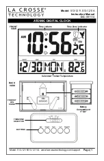
Brand: La Crosse Technology Pages: 2
404-1246
Brand: La Crosse Technology Pages: 2
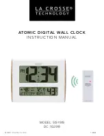
513-1211
Brand: La Crosse Technology Pages: 4

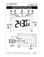
513-149V2
Brand: La Crosse Technology Pages: 10
W88631
Brand: La Crosse Technology Pages: 2
513-1919
Brand: La Crosse Technology Pages: 10
519-1416
Brand: La Crosse Pages: 6


