


SERVICE MANUAL
Sec. 1: Main Section
I
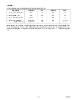
Specifications
I
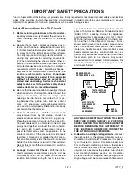
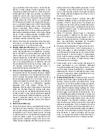
Preparation for Servicing
I
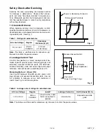
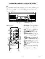
Adjustment Procedures
I
Schematic Diagrams
I
CBA’s
Sec. 2: Deck Mechanism Section
I
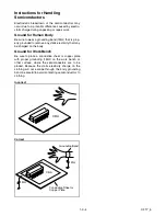
Standard Maintenance
I
Alignment for Mechanism
I
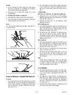
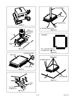
Disassembly/Assembly of Mechanism
Sec. 3: Exploded views
and Parts List Section
I
Exploded views
I
Parts List
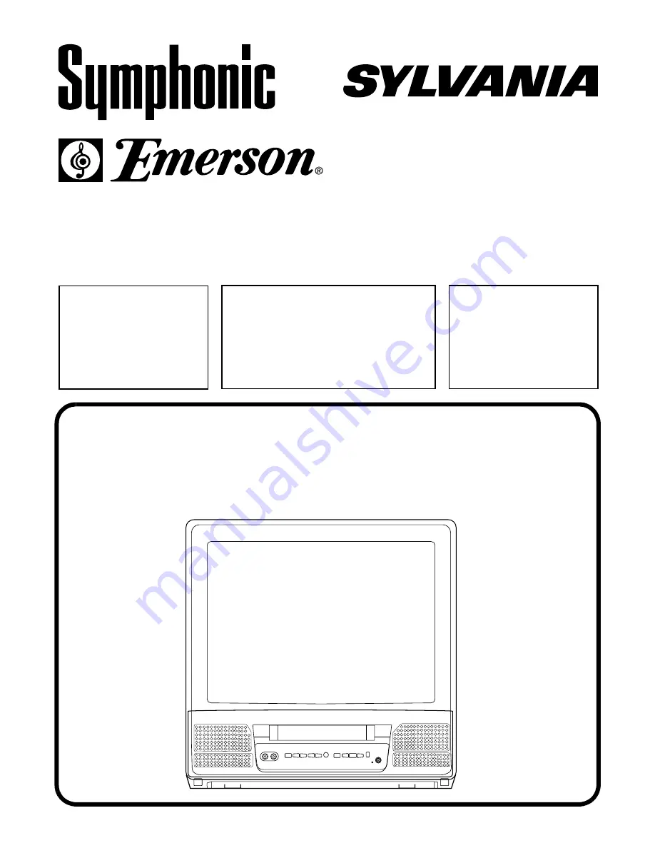
19" COLOR TV/VCR COMBINATION
SC319C/6319CC/EWC1902
Summary of Contents for 6319CC
Page 18: ...1 6 2 T7300DC Fig 1 ANT S 1 S 1 1 REAR CABINET S 1 S 1 S 1 S 1 Fig 2 ...
Page 20: ...1 6 4 T7300DC Fig 4 S 5 S 5 S 5 S 5 5 CRT CRT CBA ANODE CAP ...
Page 75: ...Packing X 1 S 1 S 4 S 3 S 3 S 2 TAPE TAPE X 4 X 3 X 2 X 7 S 6 S 14 FRONT 3 1 3 T7300PEX ...
Page 92: ...Printed in Japan 2002 02 20 HO SC319C 6319CC EWC1902 T7300UA 2UC 3UD ...


