background image


Last Updated: May 7, 2021


PICO-APL4 


PICO-ITX  Board 


User’s Manual 

7

th

 Ed

Summary of Contents for AAEON PICO-APL4

Page 1: ...Last Updated May 7 2021 PICO APL4 PICO ITX Board User s Manual 7th Ed ...

Page 2: ...n this manual is intended to be accurate and reliable However the original manufacturer assumes no responsibility for its use or for any infringements upon the rights of third parties that may result from its use The material in this document is for product information only and is subject to change without notice While reasonable efforts have been made in the preparation of this document to assure...

Page 3: ...stered trademark of Microsoft Corp Intel Pentium and Celeron are registered trademarks of Intel Corp Intel Atom is a trademark of Intel Corp ITE is a trademark of Integrated Technology Express Inc IBM PC AT PS 2 and VGA are trademarks of International Business Machines Corporation All other product names or trademarks are properties of their respective owners ...

Page 4: ...Packing List Before setting up your product please make sure the following items have been shipped Item Quantity PICO APL4 1 If any of these items are missing or damaged please contact your distributor or sales representative immediately ...

Page 5: ...escriptions and explanations on the product s hardware and software features if any its specifications dimensions jumper connector settings definitions and driver installation instructions if any to facilitate users in setting up their product Users may refer to the product page at AAEON com for the latest version of this document ...

Page 6: ...nsient over voltage 7 Always disconnect this device from any AC supply before cleaning 8 While cleaning use a damp cloth instead of liquid or spray detergents 9 Make sure the device is installed near a power outlet and is easily accessible 10 Keep this device away from humidity 11 Place the device on a solid surface during installation to prevent falls 12 Do not cover the openings on the device to...

Page 7: ...intrusion to the device iii Exposure to moisture iv Device is not working as expected or in a manner as described in this manual v The device is dropped or damaged vi Any obvious signs of damage displayed on the device 18 DO NOT LEAVE THIS DEVICE IN AN UNCONTROLLED ENVIRONMENT WHERE THE STORAGE TEMPERATURE IS BELOW 20 C 4 F OR ABOVE 60 C 140 F TO PREVENT DAMAGE ...

Page 8: ...sion if the battery is incorrectly replaced Replace only with the same or equivalent type recommended by the manufacturer Dispose of used batteries according to the manufacturer s instructions and your local government s recycling or disposal directives Attention Il y a un risque d explosion si la batterie est remplacée de façon incorrecte Ne la remplacer qu avec le même modèle ou équivalent recom...

Page 9: ...素名称及含量 AAEON Main Board Daughter Board Backplane 部件名称 有毒有害物质或元素 铅 Pb 汞 Hg 镉 Cd 六价铬 Cr VI 多溴联苯 PBB 多溴二苯醚 PBDE 印刷电路板 及其电子组件 外部信号 连接器及线材 O 表示该有毒有害物质在该部件所有均质材料中的含量均在 SJ T 11363 2006 标准规定的限量要求以下 X 表示该有毒有害物质至少在该部件的某一均质材料中的含量超出 SJ T 11363 2006 标准规定的限量要求 备注 此产品所标示之环保使用期限 系指在一般正常使用状况下 ...

Page 10: ...yl Ethers PBDE PCB Other Components O O O O O Wires Connectors for External Connections O O O O O O O The quantity of poisonous or hazardous substances or elements found in each of the component s parts is below the SJ T 11363 2006 stipulated requirement X The quantity of poisonous or hazardous substances or elements found in at least one of the component s parts is beyond the SJ T 11363 2006 stip...

Page 11: ...4 1 COM Port 2 CN1 13 2 4 2 COM Port 1 CN2 15 2 4 3 Front Panel Connector CN3 16 2 4 4 M 2 Key E Slot 2230 CN4 16 2 4 5 M 2 Key B Slot 2280 CN5 19 2 4 6 BIO Port Optional CN6 22 2 4 7 Digital I O CN7 25 2 4 8 SATA Port CN8 26 2 4 9 SPI Flash Programming Port CN9 27 2 4 10 5V Output for SATA HDD CN12 27 2 4 11 HDMI Port CN11 28 2 4 12 Battery CN12 29 2 4 13 LAN RJ 45 Port1 CN13 29 2 4 14 LAN RJ 45 ...

Page 12: ...01 40 Chapter 3 AMI BIOS Setup 41 3 1 System Test and Initialization 42 3 2 AMI BIOS Setup 43 3 3 Setup Submenu Main 44 3 4 Setup Submenu Advanced 45 3 4 1 Trusted Computing 46 3 4 2 CPU Configuration 48 3 4 3 SATA Configuration 50 3 4 4 Hardware Monitor 51 3 4 5 SIO Configuration 52 3 4 5 1 Serial Port 1 Configuration 53 3 4 5 2 Serial Port 2 Configuration 54 3 4 5 Digital IO Port Configuration 5...

Page 13: ... 64 3 7 1 BBS Priorities 65 3 8 Setup Submenu Save Exit 66 Chapter 4 Drivers Installation 67 4 1 Driver Download Installation 68 Appendix A I O Information 70 A 1 I O Address Map 71 A 2 Memory Address Map 72 A 3 IRQ Mapping Chart 73 Appendix B Mating Connectors 76 B 1 List of Mating Connectors and Cables 77 ...

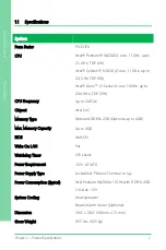
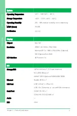
Page 14: ...Pico ITX Board PICO APL4 Chapter 1 Chapter 1 Product Specifications ...

Page 15: ...DP 12W CPU Frequency Up to 2 4GHz Chipset Intel SoC Memory Type Onboard DDR3L 2GB Optional up to 4GB Max Memory Capacity Up to 4GB BIOS AMI SPI Wake On LAN Yes Watchdog Timer 255 Levels Power Requirement 12V AT ATX Power Supply Type Lockable Phoenix Terminal co lay Power Consumption Typical Intel Pentium N4200 at 1 1GHz with DDR3L 4GB 1 43A at 12V System Cooling Heat spreader Heatsink with cooler ...

Page 16: ...FCC Display Chipset Intel SoC Resolution HDMI 1 4b 3840 x 2160 30Hz Internal eDP 1 4 3840 x 2160 60Hz Optional DDI Optional from BIO LCD Interface eDP version 1 4 I O Storage SSD SATA 6 0 Gb s x 1 5V Power reserved M 2 2280 B Key x 1 eMMC 32GB Optional 16GB 64GB 128GB Ethernet Realtek 8111G x 2 USB Port USB 3 2 Gen 1 x 2 Rear IO USB 2 0 x 2 Internal co use with FAN connector Serial Port COM1 RS 23...

Page 17: ...Chapter 1 Product Specifications 4 Pico ITX Board PICO APL4 I O Expansion Slot M 2 2230 x 1 E Key BIO x 1 optional I2C Smbus SIM TPM Touch ...

Page 18: ...Pico ITX Board PICO APL4 Chapter 2 Chapter 2 Hardware Information ...

Page 19: ...Chapter 2 Hardware Information 6 Pico ITX Board PICO APL4 2 1 Dimensions Component Side Component Side ...

Page 20: ...Chapter 2 Hardware Information 7 Pico ITX Board PICO APL4 Solder Side Solder Side ...

Page 21: ...Chapter 2 Hardware Information 8 Pico ITX Board PICO APL4 Rear I O Configuration Phoenix DC Jack ...

Page 22: ...Chapter 2 Hardware Information 9 Pico ITX Board PICO APL4 2 2 Jumpers and Connectors Component Side Component Side ...

Page 23: ...Chapter 2 Hardware Information 10 Pico ITX Board PICO APL4 Solder Side Solder Side ...

Page 24: ...n configure for your application Label Function JP1 Auto Power Button Enable Disable Selection JP2 Clear CMOS Jumper 2 3 1 Auto Power Button Enable Disable Selection JP1 Enable AT Default Disable ATX Note When disabled the power button of CN3 1 2 is used to power on the system 2 3 2 Clear CMOS Jumper JP2 Clear CMOS Normal Default 1 2 3 1 2 3 1 2 3 1 2 3 ...

Page 25: ... COM Port 1 CN3 Front Panel Connector CN4 M 2 Key E Slot 2230 CN5 M 2 Key B Slot 2280 CN6 BIO Port Optional CN7 Digital I O CN8 SATA Port CN9 SPI Flash Programming Port CN10 5V Output for SATA HDD CN11 HDMI Port CN12 Battery CN13 LAN RJ 45 Port1 CN14 LAN RJ 45 Port2 CN15 USB 3 0 Ports 0 and 1 CN17 External Power Input CN18 12V DC Power Jack Optional CN19 Embedded DisplayPort Optional CN20 USB 2 0 ...

Page 26: ...tion 13 Pico ITX Board PICO APL4 2 4 1 COM Port 2 CN1 RS232 Pin Pin Name Signal Type Signal Level 1 DCD2 IN 2 DSR2 IN 3 RX2 IN 4 RTS2 OUT 5V 5 TX2 OUT 5V 6 CTS2 IN 7 DTR2 OUT 5V 8 RI2 5V 12V IN 5V 12V 9 GND GND 1 2 3 4 5 6 7 8 9 ...

Page 27: ..._D2 I O 5V 4 NC 5 NC 6 NC 7 NC 8 NC 5V 12V PWR 5V 12V 9 GND GND RS422 Pin Pin Name Signal Type Signal Level 1 RS422_TX2 OUT 5V 2 NC 3 RS422_TX2 OUT 5V 4 NC 5 RS422_RX2 IN 6 NC 7 RS422_RX2 IN 8 NC 5V 12V PWR 5V 12V 9 GND GND Note COM2 RS 232 422 485 can be set by BIOS setting Default is RS 232 Note Pin 8 function can be changed by BOM ...

Page 28: ...Information 15 Pico ITX Board PICO APL4 2 4 2 COM Port 1 CN2 RS232 Pin Pin Name Signal Type Signal Level 1 DCD1 IN 2 DSR1 IN 3 RX1 IN 4 RTS1 OUT 9V 5 TX1 OUT 9V 6 CTS1 IN 7 DTR1 OUT 9V 8 RI1 IN 9 GND GND 1 2 3 4 5 6 7 8 9 ...

Page 29: ... Pin Pin Name 1 PWR_BTN 2 PWR_BTN 3 HDD_LED 4 HDD_LED 5 SPEAKER 6 SPEAKER 7 PWR_LED 8 PWR_LED 9 H W RESET 10 H W RESET 2 4 4 M 2 Key E Slot 2230 CN4 Pin Pin Name Signal Type Signal Level 1 GND GND 2 3 3VSB PWR 3 3V 3 USB_D DIFF 4 3 3VSB PWR 3 3V 5 USB_D DIFF 6 NC 7 GND GND 8 NC 9 NC 10 NC 11 NC 1 10 2 9 ...

Page 30: ... APL4 Pin Pin Name Signal Type Signal Level 12 NC 13 NC 14 NC 15 NC 16 NC 17 NC 18 NC 19 NC 20 NC 21 NC 22 NC 23 NC 32 NC 33 GND GND 34 NC 35 PCIE_TX DIFF 36 NC 37 PCIE_TX DIFF 38 NC 39 GND GND 40 NC 41 PCIE_RX DIFF 42 NC 43 PCIE_RX DIFF 44 NC 45 GND GND ...

Page 31: ...Level 46 NC 47 PCIE_REF_CLK DIFF 48 NC 49 PCIE_REF_CLK DIFF 50 NC 51 GND GND 52 PCIE_RST OUT 3 3V 53 PCIE_CLK_REQ IN 3 3V 54 W_DISABLE2 OUT 3 3V 55 PCIE_WAKE IN 3 3V 56 W_DISABLE1 OUT 3 3V 57 GND GND 58 NC 59 NC 60 NC 61 NC 62 NC 63 GND GND 64 NC 65 NC 66 NC 67 NC 68 NC 69 GND GND 70 NC 71 NC ...

Page 32: ... 72 3 3VSB PWR 3 3V 73 NC 74 3 3VSB PWR 3 3V 75 GND GND 2 4 5 M 2 Key B Slot 2280 CN5 Pin Pin Name Signal Type Signal Level 1 GND GND 2 3 3V PWR 3 3V 3 GND GND 4 3 3V PWR 3 3V 5 GND GND 6 NC 7 USB_D DIFF 8 NC 9 USB_D DIFF 10 SSD_DAS IN 3 3V 11 GND GND 20 NC 21 GND GND 22 NC 23 NC 24 NC 25 NC 26 NC ...

Page 33: ...in Name Signal Type Signal Level 27 GND GND 28 NC 29 NC 30 NC 31 NC 32 NC 33 GND GND 34 NC 35 NC 36 NC 37 NC 38 DEVSLP OUT 1 8V 39 GND GND 40 NC 41 SATA_RX DIFF 42 NC 43 SATA_RX DIFF 44 NC 45 GND GND 46 NC 47 SATA_TX DIFF 48 NC 49 SATA_TX DIFF 50 NC 51 GND GND 52 NC ...

Page 34: ... PICO APL4 Pin Pin Name Signal Type Signal Level 53 NC 54 NC 55 NC 56 NC 57 GND GND 58 NC 59 NC 60 NC 61 NC 62 NC 63 GND GND 64 NC 65 NC 66 NC 67 NC 68 NC 69 GND GND 70 3 3V PWR 3 3V 71 GND GND 72 3 3V PWR 3 3V 73 GND GND 74 3 3V PWR 3 3V 75 GND GND ...

Page 35: ...2 4 6 BIO Port Optional CN6 Pin Pin Name Signal Type Signal Level 1 12VSB PWR 12V 2 GND GND 3 GND GND 4 PCIE_TXN0 DIFF 5 PCIE_RXN0 DIFF 6 PCIE_TXP0 DIFF 7 PCIE_RXP0 DIFF 8 GND GND 9 GND GND 10 PCIE_TXN1 DIFF 11 PCIE_RXN1 DIFF 12 PCIE_TXP1 DIFF 13 PCIE_RXP1 DIFF ...

Page 36: ...O 3 3V 18 DDI_DDCDATA I O 3 3V 19 5VSB PWR 5V 20 5VSB PWR 5V 21 5VSB PWR 5V 22 5VSB PWR 5V 23 PCIE_REF_CLK0 DIFF 24 RESET OUT 25 PCIE_REF_CLK0 DIFF 26 GND GND 27 GND GND 28 DDI_TX1N DIFF 29 DDI_TX0N DIFF 30 DDI_TX1P DIFF 31 DDI_TX0P DIFF 32 GND GND 33 GND GND 34 DDI_TX3N DIFF 35 DDI_TX2N DIFF 36 DDI_TX3P DIFF 37 DDI_TX2P DIFF 38 GND GND 39 GND GND ...

Page 37: ...DI0_AUXP DIFF 44 USB3_TX_N DIFF 45 GND GND 46 USB3_TX_P DIFF 47 USB_D0 DIFF 48 GND GND 49 USB_D0 DIFF 50 USB3_RX_N DIFF 51 GND GND 52 USB3_RX_P DIFF 53 SMB_CLK I O 3 3V 54 GND GND 55 SMB_DATA I O 3 3V 56 WAKE IN 3 3V 57 GND GND 58 USB_OC IN 3 3V 59 5V PWR 5V 60 USB_OC IN 3 3V 61 5V PWR 5V 62 5V PWR 5V 63 5V PWR 5V 64 5V PWR 5V 65 LPC_AD0 I O 3 3V ...

Page 38: ..._FRAME IN 3 3V 67 LPC_AD1 I O 3 3V 68 SERIRQ I O 3 3V 69 LPC_AD2 I O 3 3V 70 NC 71 LPC_AD3 I O 3 3V 72 BIO_PWOK IN 3 3V 73 GND GND 74 NC 75 LPC_CLK OUT 3 3V 76 NC 77 NC 78 NC 79 GND GND 80 GND GND 2 4 7 Digital I O CN7 Pin Pin Name Signal Type Signal Level 1 5V PWR 5V 2 DIO0 I O 5V 3 DIO1 I O 5V 1 5 2 6 ...

Page 39: ...rd PICO APL4 Pin Pin Name Signal Type Signal Level 4 DIO2 I O 5V 5 DIO3 I O 5V 6 GND GND 2 4 8 SATA Port CN8 Pin Pin Name Signal Type Signal Level 1 GND GND 2 SATA_TX DIFF 3 SATA_TX DIFF 4 GND GND 5 SATA_RX DIFF 6 SATA_RX DIFF 7 GND GND Pin 1 Pin 7 ...

Page 40: ...g Port CN9 Pin Pin Name Signal Type Signal Level 1 SPI_MISO OUT 2 GND GND 3 SPI_CLK IN 4 3 3VSB PWR 3 3V 5 SPI_MOSI IN 6 SPI_CS IN 7 NC 2 4 10 5V Output for SATA HDD CN12 Pin Pin Name Signal Type Signal Level 1 5V PWR 5V 2 GND GND P IN 1 P IN 2 P IN 3 P IN 4 P IN 5 P IN 6 P IN 7 5V GND ...

Page 41: ...nal Type Signal level 1 TMDS_DAT2 DIFF 2 GND GND 3 TMDS_DAT2 DIFF 4 TMDS_DAT1 DIFF 5 GND GND 6 TMDS_DAT1 DIFF 7 TMDS_DAT0 DIFF 8 GND GND 9 TMDS_DAT0 DIFF 10 TMDS_CLK DIFF 11 GND GND 12 TMDS_CLK DIFF 13 NC 14 NC 15 DDC_CLK I O 5V 16 DDC_DATA I O 5V 17 GND GND 18 5V I O 5V 19 HPLG_DETECT IN 1 2 18 19 ...

Page 42: ... Battery CN12 Pin Pin Name Signal Type Signal Level 1 3 3V PWR 3 3V 2 GND GND 2 4 13 LAN RJ 45 Port1 CN13 Pin Pin Name Signal Type Signal level 1 MDI0 DIFF 2 MDI0 DIFF 3 MDI1 DIFF 4 MDI2 DIFF 5 MDI2 DIFF 6 MDI1 DIFF 7 MDI3 DIFF 8 MDI3 DIFF 1 ACT LINK LED SPEED LED 8 ...

Page 43: ...rmation 30 Pico ITX Board PICO APL4 2 4 14 LAN RJ 45 Port2 CN14 Pin Pin Name Signal Type Signal Level 1 MDI0 DIFF 2 MDI0 DIFF 3 MDI1 DIFF 4 MDI2 DIFF 5 MDI2 DIFF 6 MDI1 DIFF 7 MDI3 DIFF 8 MDI3 DIFF 1 ACT LINK LED SPEED LED 8 ...

Page 44: ...el 1 5VSB PWR 5V 2 USB0_D DIFF 3 USB0_D DIFF 4 GND GND 5 USB0_SSRX DIFF 6 USB0_SSRX DIFF 7 GND GND 8 USB0_SSTX DIFF 9 USB0_SSTX DIFF 10 5VSB PWR 5V 11 USB1_D DIFF 12 USB1_D DIFF 13 GND GND 14 USB1_SSRX DIFF 15 USB1_SSRX DIFF 16 GND GND 17 USB1_SSTX DIFF 18 USB1_SSTX DIFF 10 Port 1 Port 0 11 12 13 1 2 3 4 14 15 16 17 18 5 6 7 8 9 ...

Page 45: ...vel 1 VIN PWR 12V 2 GND GND 2 4 17 12V DC Power Jack Optional CN18 Pin Pin Name Signal Type Signal Level 1 12V PWR 12V 2 GND GND 3 GND GND 2 4 18 Embedded DisplayPort Optional CN19 Pin Pin Name Signal Type Signal Level 1 VCC_PWR PWR 3 3V 2 VCC_PWR PWR 3 3V 3 GND GND 4 GND GND 5 EDP_TX2_N DIFF 6 EDP_TX2_P DIFF 7 GND GND VIN GND ...

Page 46: ...TX1_P DIFF 10 GND GND 11 EDP_TX0_N DIFF 12 EDP_TX0_P DIFF 13 GND GND 14 EDP_TX3_N DIFF 15 EDP_TX3_P DIFF 16 GND GND 17 EDP_AUXN DIFF 18 EDP_AUXP DIFF 19 GND GND 20 EDP_BKLTNESS OUT 3 3V 21 NC 22 EDP_BKLTEN OUT 3 3V 23 EDP_HPD IN 24 GND GND 25 GND GND 26 GND GND 27 12V PWR 12V 28 12V PWR 12V 29 12V PWR 12V 30 12V PWR 12V ...

Page 47: ...CO APL4 2 4 19 USB 2 0 Port 2 CN20 Pin Pin Name Signal Type Signal Level 1 5VSB PWR 5V 2 USB_D DIFF 3 USB_D DIFF 4 GND GND 2 4 20 USB 2 0 Port 1 CN21 Pin Pin Name Signal Type Signal Level 1 5VSB PWR 5V 2 USB_D DIFF 3 USB_D DIFF 4 GND GND 1 2 3 4 1 2 3 4 ...

Page 48: ... 3V 4 LAD3 I O 3 3V 5 3 3V PWR 3 3V 6 LFRAME IN 7 LRESET OUT 3 3V 8 GND GND 9 LCLK OUT 10 SMB_DATA I2C_SDA I O 3 3V 11 SMB_CLK I2C_SCL OUT 3 3V 12 SMB_ALERT INT_SERIRQ I O 3 3V Note I2C SMBus pins 10 11 12 can be set by Bios Option Menu BOM R406 R403 R414 I2C default R405 R408 R411 SMBus LAD0 1 12 LAD1 LAD2 LAD3 LFRAME LRESET I2C_SDA I2C_SCL SERIRQ GND LCLK 3 3V ...

Page 49: ...nal Level Rate Output COM Port 2 CN1 5V 12V 5V 0 5A or 12V 0 5A M 2 Key E Slot 2230 CN4 3 3VSB 3 3V 2A M 2 Key B Slot 2280 CN5 3 3V 3 3V 2 5A Digital IO Port CN7 5V 5V 1A 5V Output for SATA HDD CN10 5V 5V 1A USB Ports 0 and 1 CN15 5VSB 5V 1A per channel USB 2 0 Ports 2 CN20 5VSB 5V 0 5A USB 2 0 Ports 1 CN21 5VSB 5V 0 5A ...

Page 50: ...Chapter 2 Hardware Information 37 Pico ITX Board PICO APL4 2 6 Function Block ...

Page 51: ... 7 1 PICO APL4 HSK01 AAEON provides a heat spreader and a heatsink with both studs and screws included as options AAEON suggests using both for assembly Note For best performance and reliability AAEON advises enabling a power limit in BIOS setup when using a passive cooling solution ...

Page 52: ...nformation 39 Pico ITX Board PICO APL4 2 7 2 PICO APL4 HSP01 If installing the PICO APL4 onto a chassis with only the heat spreader provided by AAEON make sure to apply thermal grease between the heat spreader and chassis ...

Page 53: ...Chapter 2 Hardware Information 40 Pico ITX Board PICO APL4 2 7 3 PICO APL4 FAN01 Note The active cooling solution can be operated via 5V USB power from CN20 or CN21 without fan speed control ...

Page 54: ...Pico ITX Board PICO APL4 Chapter 3 Chapter 3 AMI BIOS Setup ...

Page 55: ...CMOS memory and BIOS NVRAM If system configuration is not found or system configuration data error is detected system will load optimized default and re boot with this default system configuration automatically There are four situations in which you will need to setup system configuration 1 You are starting your system for the first time 2 You have changed the hardware attached to your system 3 Th...

Page 56: ... power is turned off Entering Setup Power on the computer and press Del or ESC immediately This will allow you to enter Setup Main Date and time can be set here Press Tab to switch between date elements Advanced Access and configure advanced processor options and features Chipset Chipset and host bridge options and features Boot Set boot options including boot priority and Quiet Boot option Securi...

Page 57: ...Chapter 3 AMI BIOS Setup 44 Pico ITX Board PICO APL4 3 3 Setup Submenu Main ...

Page 58: ...Chapter 3 AMI BIOS Setup 45 Pico ITX Board PICO APL4 3 4 Setup Submenu Advanced ...

Page 59: ...lable SHA 1 PCR Bank Disable Enable Optimal Default Failsafe Default Enable or Disable SHA 1 PCR Bank SHA256 PCR Bank Disable Enable Optimal Default Failsafe Default Enable or Disable SHA256 PCR Bank Pending Operation None Optimal Default Failsafe Default TPM Clear Schedule an Operation for the Security Device NOTE Your Computer will reboot during restart in order to change State of Security Devic...

Page 60: ...Default Enable or Disable Endorsement Hierarchy TPM2 0 UEFI Spec Version TCG_1_2 TCG_2 Optimal Default Failsafe Default Select the TCG2 Spec Version Support TCG_1_2 the Compatible mode for Win8 Win10 TCG_2 Support new TCG2 protocol and event format for Win10 or later Physical Presence Spec Version 1 2 1 3 Optimal Default Failsafe Default Select to Tell O S to support PPI Spec Version 1 2 or 1 3 No...

Page 61: ...t Failsafe Default Enable Disable Intel SpeedStep Turbo Mode Disabled Enabled Optimal Default Failsafe Default Turbo Mode Intel Virtualization Technology Disabled Enabled Optimal Default Failsafe Default When enabled a VMM can utilize the additional hardware capabilities provided by Vanderpool Technology VT d Disabled Optimal Default Failsafe Default Enabled Enable Disable CPU VT d Table Continues...

Page 62: ...Chapter 3 AMI BIOS Setup 49 Pico ITX Board PICO APL4 Options Summary Power Limit 1 Enable Disabled Optimal Default Failsafe Default Enabled Enable Disable Power Limit 1 ...

Page 63: ...ATA GEN SPEED AUTO Optimal Default Failsafe Default GEN1 GEN2 GEN3 SATA GEN SPEED SELECTION Port0 M 2 port Disabled Enabled Optimal Default Failsafe Default Enable Disable SATA port SATA Port 0 Hot Plug Capability Disabled Optimal Default Failsafe Default Enabled Enable Disable SATA port hot plug ...

Page 64: ...Chapter 3 AMI BIOS Setup 51 Pico ITX Board PICO APL4 3 4 4 Hardware Monitor ...

Page 65: ...Chapter 3 AMI BIOS Setup 52 Pico ITX Board PICO APL4 3 4 5 SIO Configuration ...

Page 66: ...This Device Disable Enable Optimal Default Failsafe Default Enable or Disable this Logical Device Possible Use Automatic Settings Optimal Default Failsafe Default IO 3F8h IRQ 4 IO 2F8h IRQ 3 Allows user to change Device s Resource settings New settings will be reflected on This Setup Page after System restarts ...

Page 67: ...This Device Disable Enable Optimal Default Failsafe Default Enable or Disable this Logical Device Possible Use Automatic Settings Optimal Default Failsafe Default IO 2F8h IRQ 3 IO 3F8h IRQ 4 Allows user to change Device s Resource settings New settings will be reflected on This Setup Page after System restarts ...

Page 68: ...p 55 Pico ITX Board PICO APL4 3 4 5 Digital IO Port Configuration Options Summary DIO Port Output Input Set DIO as Input or Output Output Level High Optimal Default Failsafe Default Low Set output level when DIO pin is output ...

Page 69: ...afe Default AT Type Select system power mode Restore AC Power Loss Last State Optimal Default Failsafe Default Always On Always Off Determine the system turn on or off after AC resume from G3 to S5 state RTC wake system from S5 Disable Optimal Default Failsafe Default Fixed Time Fixed Time System will wake on the hr min sec specified ...

Page 70: ...Chapter 3 AMI BIOS Setup 57 Pico ITX Board PICO APL4 3 5 Setup Submenu Chipset ...

Page 71: ...Chapter 3 AMI BIOS Setup 58 Pico ITX Board PICO APL4 3 5 1 North Bridge ...

Page 72: ...t Disable Enable Optimal Default Failsafe Default Auto Control the PCI Express Root Port AUTO To disable unused root port automatically for the most optimum power savings Enable Enable PCIe root port Disable Disable PCIe root port M 2 PCIe Speed Auto Optimal Default Failsafe Default Gen1 Gen2 Configure PCIe Speed ...

Page 73: ... the user enters the Setup utility A User Password does not provide access to many of the features in the Setup utility Select the password you wish to set and press Enter In the dialog box enter your password must be between 3 and 20 letters or numbers Press Enter and retype your password to confirm Press Enter again to set the password Removing the Password Select the password you want to remove...

Page 74: ...is in User mode The mode change requires platform reset Secure Boot Mode Custom Optimal Default Failsafe Default Standard Secure Boot mode options Standard or Custom In Custom mode Secure Boot Policy variables can be configured by a physically present user without full authentication Restore Factory Keys Force System to User Mode Install factory default Secure Boot key databases Reset To Setup Mod...

Page 75: ...s Force System to User Mode Install factory default Secure Boot key databases Reset To Setup Mode Delete all Secure Boot key databases from NVRAM Export Secure Boot variables Copy NVRAM content of Secure Boot variables to files in a root folder on a file system device Enroll Efi Image Allow the image to run in Secure Boot mode Enroll SHA256 Hash certificate of a PE image into Authorized Signature ...

Page 76: ...ized Signatures Details Export Update Append Delete Forbidden Signatures Details Export Update Append Delete Authorized Time Stamps Update Append OsRecovery Signatures Update Append Enroll Factory Defaults or load certificates from a file 1 Public Key Certificate a EFI_SIGNATURE_LIST b EFI_CERT_X509 DER c EFI_CERT_RSA2048 bin d EFI_CERT_SHAXXX 2 Authenticated UEFI Variable 3 EFI PE COFF Image SHA2...

Page 77: ...e Default Enables or Disables showing boot logo Monitor Mwait Disable Enabled Auto Optimal Default Failsafe Default Enable Disable Monitor Mwait To install Linux OS please set this item to disable Ipv4 PXE Support Disabled Optimal Default Failsafe Default Enabled Enable Ipv4 PXE Boot Support If disabled IPV4 PXE boot option will not be created ...

Page 78: ...Chapter 3 AMI BIOS Setup 65 Pico ITX Board PICO APL4 3 7 1 BBS Priorities ...

Page 79: ...Chapter 3 AMI BIOS Setup 66 Pico ITX Board PICO APL4 3 8 Setup Submenu Save Exit ...

Page 80: ...Pico ITX Board PICO APL4 Chapter 4 Chapter 4 Drivers Installation ...

Page 81: ... below to install them Step 1 Install Chipset Driver 1 Open the STEP1 CHIPSET folder and open the SetupChipset exe file 2 Follow the instructions 3 Drivers will be installed automatically Step 2 Install Graphic Driver 1 Open the STEP2 VGA folder and open the Setup exe file 2 Follow the instructions 3 Driver will be installed automatically Step 3 Install LAN Driver 1 Open the STEP3 LAN folder and s...

Page 82: ... STEP4 AUDIO folder and open the 0006 64bit_Win7_Win8_Win81_Win10_R279 exe file 2 Follow the instructions 3 Driver will be installed automatically Step 5 Install TXE Driver 1 Open the STEP5 TXE folder and open the SetupTXE exe file 2 Follow the instructions 3 Driver will be installed automatically ...

Page 83: ...Pico ITX Board PICO APL4 Appendix A Appendix A I O Information ...

Page 84: ...Appendix A I O Information 71 Pico ITX Board PICO APL4 A 1 I O Address Map ...

Page 85: ...Appendix A I O Information 72 Pico ITX Board PICO APL4 A 2 Memory Address Map ...

Page 86: ...Appendix A I O Information 73 Pico ITX Board PICO APL4 A 3 IRQ Mapping Chart ...

Page 87: ...Appendix A I O Information 74 Pico ITX Board PICO APL4 ...

Page 88: ...Appendix A I O Information 75 Pico ITX Board PICO APL4 ...

Page 89: ...Pico ITX Board PICO APL4 Appendix B Appendix B Mating Connectors ...

Page 90: ...tor JCTC 11002H00 5 2P N A N A CN7 Digital I O Connector Harwin M50 3000345 N A N A CN8 SATA Connector Molex 887505318 SATA Cable 1709070500 CN10 5Vout Connector JST PHR 2 2 Pins for SATA HDD Power 1702150155 CN12 External RTC Connector Molex 51021 0200 Battery Cable 175011301C CN17 Power Input Connector Molex 19211 0003 Power Cable 170204010R CN19 Embedded DisplayPort Connector KEL SSL20 30S N A ...

Reviews: