background image


Last Updated: May 14, 2021


OMNI-2155-CML 


Industrial  Touch  Panel 

with  10

th


Generation  Intel®  Core™  Processors


User’s  Manual 

1

st

  Ed

Summary of Contents for AAEON OMNI-2155-CML

Page 1: ...Last Updated May 14 2021 OMNI 2155 CML Industrial Touch Panel with 10th Generation Intel Core Processors User s Manual 1st Ed ...

Page 2: ...ided in this manual is intended to be accurate and reliable However the original manufacturer assumes no responsibility for its use or for any infringements upon the rights of third parties that may result from its use The material in this document is for product information only and is subject to change without notice While reasonable efforts have been made in the preparation of this document to ...

Page 3: ...ows is a registered trademark of Microsoft Corp Intel Pentium and Celeron are registered trademarks of Intel Corporation Intel Core is a trademark of Intel Corporation All other product names or trademarks are properties of their respective owners The publisher of this document does not assume nor imply ownership of any trademarked product not listed herein ...

Page 4: ... setting up your product please make sure the following items have been shipped Item Quantity OMNI 2155 CML 1 Screw Package 1 3 Pin DC In Power Connector 1 If any of these items are missing or damaged please contact your distributor or sales representative immediately ...

Page 5: ...iled descriptions and explanations on the product s hardware and software features if any its specifications dimensions jumper connector settings definitions and driver installation instructions if any to facilitate users in setting up their product Users may refer to the product page at AAEON com for the latest version of this document ...

Page 6: ...y transient over voltage 7 Always disconnect this device from any power supply before cleaning 8 While cleaning use a damp cloth instead of liquid or spray detergents 9 Make sure the device is installed near a power outlet and is easily accessible 10 Keep this device away from humidity 11 Place the device on a solid surface during installation to prevent falls 12 Do not cover the openings on the d...

Page 7: ...so as not to damage the system or void your warranty 20 If the thermal pad had been damaged please contact AAEON s salesperson to purchase a new one Do NOT use those of other brands 21 The Hex Cylinder Coppers on the front panel are not removable 22 Repeatedly assemble and disassemble the system may cause damages to the exterior paint and surface and screw holes 23 Use the right size screwdriver 2...

Page 8: ... explosion if the battery is incorrectly replaced Replace only with the same or equivalent type recommended by the manufacturer Dispose of used batteries according to the manufacturer s instructions and your local government s recycling or disposal directives Attention Il y a un risque d explosion si la batterie est remplacée de façon incorrecte Ne la remplacer qu avec le même modèle ou équivalent...

Page 9: ...物质或元素 铅 Pb 汞 Hg 镉 Cd 六价铬 Cr VI 多溴联苯 PBB 多溴二苯 醚 PBDE 印刷电路板 及其电子组件 外部信号 连接器及线材 外壳 中央处理器 与内存 硬盘 液晶模块 光驱 触控模块 电源 电池 本表格依据 SJ T 11364 的规定编制 表示该有毒有害物质在该部件所有均质材料中的含量均在 GB T 26572标准规定的限量要求以下 表示该有害物质的某一均质材料超出了GB T 26572的限量要求 然而该 部件 仍符合欧盟指令2011 65 EU 的规范 备注 一 此产品所标示之环保使用期限 系指在一般正常使用状况下 二 上述部件物质中央处理器 内存 硬盘 光驱 电源为选购品 三 上述部件物质液晶模块 触控模块仅一体机产品适用 ...

Page 10: ... O O PSU X O O O O O Battery X O O O O O This form is prepared in compliance with the provisions of SJ T 11364 O The level of toxic or hazardous materials present in this component and its parts is below the limit specified by GB T 26572 X The level of toxic of hazardous materials present in the component exceed the limits specified by GB T 26572 but is still in compliance with EU Directive 2011 6...

Page 11: ...n JP3 9 2 3 4 4 5 8 Wire Selection 10 2 3 5 Auto Power Button Selection JP3 10 2 4 List of Connectors 11 2 4 1 LVDS Port CN1 12 2 4 2 LVDS Inverter CN2 13 2 4 3 SATA Port CN3 13 2 4 4 HDMI Port CN4 14 2 4 5 VGA Port Wafer Box Optional 14 2 4 6 LAN1 LAN2 Port CN6 CN7 14 2 4 7 Touch Screen Lines CN8 15 2 4 8 NGFF M Key 2280 CN10 15 2 4 9 NGFF E Key 2230 CN11 16 2 4 10 Power Button Wafer Reserve CN12...

Page 12: ...rt Wafer Box Optional CN55 25 2 4 25 COM3 Port Wafer Box Optional CN61 26 2 4 26 Front Panel JP7 27 2 4 27 LPC Port LPC1 27 2 4 28 Mini Card Slot Full Sized PCIe1 28 2 4 29 SIM Slot SIM1 30 2 5 CPU Installation 31 2 6 RAM and 2 5 Storage Drive installation 32 Chapter 3 AMI BIOS Setup 34 3 1 System Test and Initialization 35 3 2 AMI BIOS Setup 36 3 3 Setup Submenu Main 37 3 4 Setup Submenu Advanced...

Page 13: ...p Submenu Chipset 54 3 5 1 System Agent SA Configuration 55 3 5 1 1 LVDS Panel Configuration 57 3 5 2 PCH IO Configuration 58 3 6 Setup Submenu Security 60 3 6 1 Secure Boot 61 3 6 1 1 Key Management 62 3 7 Setup Submenu Boot 64 3 8 Setup Submenu Save Exit 65 Chapter 4 Drivers Installation 66 4 1 Drivers Download and Installation 67 Appendix A Watchdog Timer Programming 69 A 1 Watchdog Timer Initi...

Page 14: ...Industrial Touch Panel OMNI 2155 CML Chapter 1 Chapter 1 Product Specifications ...

Page 15: ...thernet Intel i211 x 1 Intel i219 x 1 I O Port HDMI x 1 RJ 45 x 2 for GbE LAN i211 x 1 i219 x 1 USB 3 2 Gen 2 x 4 DB 9 x 2 for RS 232 422 485 Line out x 1 3 pin 10 35V Power Input x 1 Power Button with LED x 1 Storage Disk Drive M 2 2280 slot x 1 PCIe 3 0 x4 NVMe support 2 5 SATA SSD HDD bay x 1 Expansion Slot M 2 2230 E Key x 1 M 2 2280 B Key x 1 Full Size Mini Card x1 mSATA PCIe switch by BIOS d...

Page 16: ...rating Temperature 0 C 45 C 35W CPU according to IEC68 2 14 with 0 5 m s airflow Storage Temperature 4 F 158 F 20 C 70 C Storage Humidity 90 40 C non condensing Vibration 1 Grms 5 500Hz random operation Shock 15G peak acceleration duration 11 ms EMC CE FCC Class A Power Supply DC Input 10 35V LCD Display Type 15 6 TFT LCD LED Max Resolution 1366 H x 768 V Max Colors 16 7M 8 bit color Luminance 400...

Page 17: ...Chapter 1 Product Specifications 4 Industrial Touch Panel OMNI 2155 CML Touchscreen Type Flat 5 wire Resistive P CAP Multi Touch Light Transmission 80 3 88 2 ...

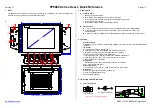
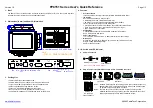
Page 18: ...Industrial Touch Panel OMNI 2155 CML Chapter 2 Chapter 2 Hardware Information ...

Page 19: ...Chapter 2 Hardware Information 6 Industrial Touch Panel OMNI 2155 CML 2 1 Dimensions Main Panel ...

Page 20: ...Chapter 2 Hardware Information 7 Industrial Touch Panel OMNI 2155 CML Board Dimensions ...

Page 21: ...Chapter 2 Hardware Information 8 Industrial Touch Panel OMNI 2155 CML 2 2 Jumpers and Connectors ...

Page 22: ...u can configure for your application Label Function JP1 Clear CMOS JP2 LVDS BKLT Power JP3 LVDS BKLT Control Selection JP4 4 5 8 Wire Selection JP6 Auto Power Button Selection 2 3 1 Clear CMOS JP1 Normal Default Clear CMOS 2 3 2 LVDS BKLT Power JP2 12V Default 5V 2 3 3 LVDS BKLT Control Selection JP3 VR Mode PWM Mode Default 1 2 3 1 2 3 1 2 3 1 2 3 1 2 3 1 2 3 ...

Page 23: ...Chapter 2 Hardware Information 10 Industrial Touch Panel OMNI 2155 CML 2 3 4 4 5 8 Wire Selection 4 8 Wire 5 Wire Default 2 3 5 Auto Power Button Selection JP3 ATX Default AT 1 2 3 1 2 3 1 2 3 1 2 3 ...

Page 24: ...CN1 LVDS Port CN2 LVDS Inverter CN3 SATA Port CN4 HDMI Port CN5 VGA Port Wafer CN6 LAN RJ45 Port CN7 LAN RJ45 Port CN8 Touch Screen Lines CN9 LVDS Control Touch CN10 NGFF M KEY 2280 CN11 NGFF E KEY 2230 CN12 Power Button Wafer CN13 SPI ROM Flash Wafer CN14 DIO CN15 COM1 Port CN16 COM2 Port CN17 USB2 0 Wafer CN18 USB2 0 Wafer CN19 USB3 2 Gen 2 Dual Port CN20 USB3 2 Gen 2 Dual Port CN21 Speaker CN22...

Page 25: ... Panel LPC1 Low Pin Count PCIE1 PCIe Slot SIM1 SIM card slot SW1 Power Button 2 4 1 LVDS Port CN1 Pin Signal Pin Signal 1 BKL_EN 2 BKL_CTL 3 LVDSVCC 4 GND 5 LVD_A_CLKN 6 LVD_A_CLKP 7 LVDSVCC 8 GND 9 LVD_A_TXN0 10 LVD_A_TXP0 11 LVD_A_TXN1 12 LVD_A_TXP1 13 LVD_A_TXN2 14 LVD_A_TXP2 15 LVD_A_TXN3 16 LVD_A_TXP3 17 LVD_DDC_SDA 18 LVD_DDC_SCL 19 LVD_B_TXN0 20 LVD_B_TXP0 21 LVD_B_TXN1 22 LVD_B_TXP1 23 LVD...

Page 26: ...N3 26 LVD_B_TXP3 27 LVDSVCC 28 GND 29 LVD_B_CLKN 30 LVD_B_CLKP 2 4 2 LVDS Inverter CN2 Pin Signal Pin Signal 1 VDD 2 BKL_CTL 3 GND 4 GND 5 BKL_EN 2 4 3 SATA Port CN3 Pin Pin Name Signal Type Signal Level 1 GND GND 2 SATA_TX DIFF 3 SATA_TX DIFF 4 GND GND 5 SATA_RX DIFF 6 SATA_RX DIFF 7 GND GND Pin 1 Pin 7 ...

Page 27: ...follows standard specifications 2 4 5 VGA Port Wafer Box Optional Pin Signal Pin Signal 1 VSYNC 8 GND 2 HSYNC 9 GREEN 3 10 GND 4 DDC_CLK 11 RED 5 DDC_DAT 12 GND 6 GND 13 5V 7 BLUE 2 4 6 LAN1 LAN2 Port CN6 CN7 Pin Pin Name Signal Type Signal Level 1 MDI0 DIFF 2 MDI0 DIFF 3 MDI1 DIFF 4 MDI1 DIFF 5 MDI2 DIFF ...

Page 28: ...pe Signal Level 6 MDI2 DIFF 7 MDI3 DIFF 8 MDI3 DIFF 2 4 7 Touch Screen Lines CN8 Pin Signal Pin Signal 1 GND 2 TOP EXCITE 3 BOTTOM EXCITE 4 LEFT EXCITE 5 RIGHT EXCITE 6 TOP SENSE 7 BOTTOM SENSE 8 LEFT SENSE 9 RIGHT SENSE 2 4 8 NGFF M Key 2280 CN10 CN10 M 2 M Key follows standard specifications ...

Page 29: ...ey 2230 CN11 CN11 M 2 E Key follows standard specifications 2 4 10 Power Button Wafer Reserve CN12 Pin Pin Name 1 FP_PANSWH 2 GND 2 4 11 SPI Flash Port CN13 Pin Pin Name Signal Type Signal Level 1 SPI_MISO OUT 2 GND GND 3 SPI_CLK IN 4 3 3VSB PWR 3 3V 5 SPI_MOSI IN 6 SPI_CS IN 7 NC 8 NC ...

Page 30: ...NI 2155 CML 2 4 12 DIO Port CN14 Pin Pin Name Signal Type Signal Level 1 DIO0 I O 5V 2 DIO1 I O 5V 3 DIO2 I O 5V 4 DIO3 I O 5V 5 DIO4 I O 5V 6 DIO5 I O 5V 7 DIO6 I O 5V 8 DIO7 I O 5V 9 5V PWR 5V 10 GND GND DIO1 DIO3 DIO5 DIO7 GND DIO0 1 2 9 10 DIO2 DIO4 DIO6 5V ...

Page 31: ...Hardware Information 18 Industrial Touch Panel OMNI 2155 CML 2 4 13 COM1 Port CN15 Pin Pin Name Signal Type Signal Level 1 DCD1 IN 2 RX1 IN 3 TX1 OUT 9V 4 DTR1 OUT 9V 5 6 DSR1 IN 7 RTS1 OUT 9V 8 CTS1 IN 9 RI1 IN ...

Page 32: ... Port CN16 Pin Pin Name Signal Type Signal Level 1 DCD2 IN 2 RX2 IN 3 TX2 OUT 9V 4 DTR2 OUT 9V 5 6 DSR2 IN 7 RTS2 OUT 9V 8 CTS2 IN 9 RI2 IN 2 4 15 USB2 0 Wafer Box 5P Pitch 1 25mm CN17 CN18 Pin Pin Name Signal Type Signal Level 1 5V PWR 5V 2 USBD DIFF 3 USBD DIFF 4 GND GND 5 GND GND ...

Page 33: ...ignal Level 1 5VSB PWR 5V 2 USB1_D DIFF 3 USB1_D DIFF 4 GND GND 5 USB1_SSRX DIFF 6 USB1_SSRX DIFF 7 GND GND 8 USB1_SSTX DIFF 9 USB1_SSTX DIFF 10 5VSB PWR 5V 11 USB2_D DIFF 12 USB2_D DIFF 13 GND GND 14 USB2_SSRX DIFF 15 USB2_SSRX DIFF 16 GND GND 17 USB2_SSTX DIFF 18 USB2_SSTX DIFF 10 Port 1 Port 0 11 12 13 1 2 3 4 14 15 16 17 18 5 6 7 8 9 ...

Page 34: ...pter 2 Hardware Information 21 Industrial Touch Panel OMNI 2155 CML 2 4 17 Speaker CN21 Pin Pin Name 1 SPK L 2 SPK L 2 4 18 Line Out CN22 Pin Pin Name Pin Pin Name 1 AUD_GND 2 LOUT_R 3 5V 4 HP_DET 5 LOUT_L ...

Page 35: ...l OMNI 2155 CML 2 4 19 Speaker CN23 Pin Pin Name 1 SPK R 2 SPK R 2 4 20 Audio I O Port 10P Pitch 1 25mm Pin Pin Name Signal Type Signal Level 1 MIC_L IN 2 MIC_R IN 3 GND_AUDIO GND 4 LINE_L_IN IN 5 LINE_R_IN IN 6 GND_AUDIO GND 7 LEFT_OUT OUT 8 GND_AUDIO GND ...

Page 36: ... OUT 10 5V_AUDIO PWR 5V 2 4 21 Power Input 3 pin Terminal Block Pin Pin Name Signal Type Signal Level 1 VIN PWR 10V 35V 2 GND GND 3 GND_EARTH 2 4 22 DIO Panel ID Port CN28 Pin Pin Name Signal Type Signal Level 1 PANEL_ID1 I O 5V 2 PANEL_ID2 I O 5V 3 PANEL_ID3 I O 5V DIO1 DIO3 DIO5 DIO7 GND DIO0 1 2 9 10 DIO2 DIO4 DIO6 5V ...

Page 37: ...in Name Signal Type Signal Level 4 PANEL_ID4 I O 5V 5 PANEL_ID5 I O 5V 6 PANEL_ID6 I O 5V 7 PANEL_ID7 I O 5V 8 PANEL_ID8 I O 5V 9 NC 10 NC 2 4 23 SATA Power Connector CN29 Pin Pin Name Signal Type Signal Level 1 12V PWR 12V 2 GND GND 3 GND GND 4 5V PWR 5V 12V 1 2 3 4 GND GND 5V ...

Page 38: ...rial Touch Panel OMNI 2155 CML 2 4 24 COM4 Port Wafer Box Optional CN55 Pin Pin Name Signal Type Signal Level 1 DCD4 IN 2 DSR4 IN 3 RX4 IN 4 RTS4 OUT 9V 5 TX4 OUT 9V 6 CTS4 IN 7 DTR4 OUT 9V 8 RI4 IN 9 GND GND DCD DSR RX RTS TX CTS DTR RI GND ...

Page 39: ...rial Touch Panel OMNI 2155 CML 2 4 25 COM3 Port Wafer Box Optional CN61 Pin Pin Name Signal Type Signal Level 1 DCD3 IN 2 DSR3 IN 3 RX3 IN 4 RTS3 OUT 9V 5 TX3 OUT 9V 6 CTS3 IN 7 DTR3 OUT 9V 8 RI3 IN 9 GND GND DCD DSR RX RTS TX CTS DTR RI GND ...

Page 40: ...e Pin Pin Name 1 GND 2 EXT_PWRBTN 3 SATA_LED 4 3 3V 5 FP_SPKR 6 5V 7 GND 8 PWRLED 9 GND 10 HWRST 2 4 27 LPC Port LPC1 Pin Pin Name Signal Type Signal Level 1 LAD0 I O 3 3V 2 LAD1 I O 3 3V 3 LAD2 I O 3 3V 4 LAD3 I O 3 3V 5 3 3V PWR 3 3V LAD0 1 12 LAD1 LAD2 LAD3 LFRAME LRESET LDRQ0 LDRQ1 SERIRQ GND LCLK 3 3V ...

Page 41: ...Signal Level 6 LFRAME IN 7 LRESET OUT 3 3V 8 GND GND 9 LCLK OUT 10 LDRQ0 IN 11 LDRQ1 IN 12 SERIRQ I O 3 3V 2 4 28 Mini Card Slot Full Sized PCIe1 Pin Pin Name Signal Type Signal Level 1 PCIE_WAKE IN 2 3 3V PWR 3 3V 3 NC 4 GND GND 5 NC 6 1 5V PWR 1 5V 7 PCIE_CLK_REQ IN 8 NC PWR 9 GND GND 10 NC I O ...

Page 42: ...CIE_REF_CLK DIFF 14 NC IN 15 GND GND 16 NC PWR 17 NC 18 GND GND 19 NC 20 W_DISABLE OUT 3 3V 21 GND GND 22 PCIE_RST OUT 3 3V 23 PCIE_RX DIFF 24 3 3VSB PWR 3 3V 25 PCIE_RX DIFF 26 GND GND 27 GND GND 28 1 5V PWR 1 5V 29 GND GND 30 SMB_CLK I O 3 3V 31 PCIE_TX DIFF 32 SMB_DATA I O 3 3V 33 PCIE_TX DIFF 34 GND GND 35 GND GND 36 USB_D DIFF 37 GND GND ...

Page 43: ...evel 38 USB_D DIFF 39 3 3VSB PWR 3 3V 40 GND GND 41 3 3VSB PWR 3 3V 42 NC 43 GND GND 44 NC 45 NC 46 NC 47 NC 48 1 5V PWR 1 5V 49 NC 50 GND GND 51 NC 52 3 3VSB PWR 3 3V 2 4 29 SIM Slot SIM1 Pin Pin Name Signal Type Signal Level 1 UIM_PWR PWR 2 UIM_RST IN 3 UIM_CLK IN 4 GND GND 5 UIM_VPP PWR 6 UIM_DATA I O ...

Page 44: ...re the system is powered down not in sleep mode and the power has been disconnected Also make sure the CPU is ready for installation It is best to perform installation on a flat surface with the system removed from its mounting Step 1 Remove the screws securing the heatsink in place then set the heatsink aside Step 2 Place the CPU into the CPU socket Then place the thermal pad on the CPU Step 3 Re...

Page 45: ...face with the system removed from its mounting For specifications and requirement of memory and storage devices see Chapter 1 Specifications Step 1 Separate the system from the panel by removing the screws securing the two together Step 2 Remove the Storage Drive if one has been previously installed or mounting bracket if not Then remove the blower assembly Step 3 Insert the RAM modules one at a t...

Page 46: ...Panel OMNI 2155 CML Step 5 Mount the 2 5 Storage Device to the mounting bracket securing with four screws Step 6 Secure the bracket to the chassis as shown in the diagram Step 7 Reattach the system to the panel securing with the screws removed in Step 1 ...

Page 47: ...Industrial Touch Panel OMNI 2155 CML Chapter 3 Chapter 3 AMI BIOS Setup ...

Page 48: ... the current system configuration against the values stored in the CMOS memory If they do not match an error message will be output and the BIOS setup program will need to be run to set the configuration information in memory There are three situations in which the CMOS settings will need to be set or changed Starting the system for the first time The system hardware has been changed The system co...

Page 49: ...d when the power is turned off To enter BIOS Setup press Del or ESC immediately while your computer is powering up The function for each interface can be found below Main Date and time can be set here Press Tab to switch between date elements Advanced Enable Disable boot option for legacy network devices Chipset For hosting bridge parameters Security The setup administrator password can be set her...

Page 50: ...Chapter 3 AMI BIOS Setup 37 Industrial Touch Panel OMNI 2155 CML 3 3 Setup Submenu Main ...

Page 51: ...Chapter 3 AMI BIOS Setup 38 Industrial Touch Panel OMNI 2155 CML 3 4 Setup Submenu Advanced ...

Page 52: ...e available SHA 1 PCR Bank Disable Optimal Default Failsafe Default Enable Enable or Disable SHA 1 PCR Bank SHA256 PCR Bank Disable Enable Optimal Default Failsafe Default Enable or Disable SHA 256 PCR Bank Pending operation None Optimal Default Failsafe Default TPM Clear Schedule an Operation for the Security Device NOTE Your Computer will reboot during restart in order to change state of Securit...

Page 53: ...2 Spec Version Support TCG_1_2 The Compatible mode for Win8 Win10 TCG_2 Support new TCG2 protocol and event format for Win10 or later Physical Presence Spec Version 1 2 1 3 Optimal Default Failsafe Default Select to Tell O S to support PPI Spec Version 1 2 or 1 3 Note some HCK tests might not support 1 3 Device Select TPM 1 2 TPM 2 0 Auto Optimal Default Failsafe Default TPM 1 2 will restrict supp...

Page 54: ...Active Processor Cores All Optimal Default Failsafe Default 1 Number of cores to enable in each processor package Intel SpeedStep Disabled Enabled Optimal Default Failsafe Default Allows more than two frequency ranges to be supported C states Disabled Optimal Default Failsafe Default Enabled Enable Disable CPU Power Management Allows CPU to go to C states when it s not 100 utilized Hyper Threading...

Page 55: ...ed Optimal Default Failsafe Default When Disabled ME will be put into ME Temporarily Disabled Mode AMT BIOS Features Disabled Enabled Optimal Default Failsafe Default When disabled AMT BIOS Features are no longer supported and user is no longer able to access MEBx Setup Note This option does not disable Manageability Features in FW ...

Page 56: ...3 4 3 1 Firmware Update Configuration Options Summary Me FW Image Re Flash Disabled Optimal Default Failsafe Default Enabled Enable Disable ME FW Image Re Flash function FW Update Disabled Enabled Optimal Default Failsafe Default Enable Disable ME FW Update function ...

Page 57: ...ML 3 4 3 2 PTT Configuration Options Summary TPM Device Selection dTPM Optimal Default Failsafe Default PTT Selects TPM device PTT or dTPM PTT Enables in SkuMgr dTPM 1 2 Disables PTT in SkuMgr Warning PTT dTPM will be disabled and all data saved on it will be lost ...

Page 58: ...nfiguration Options Summary M 2 Disabled Enabled Optimal Default Failsafe Default Enable or Disable SATA Port Mini Card Disabled Enabled Optimal Default Failsafe Default Enable or Disable SATA Port Port Disabled Enabled Optimal Default Failsafe Default Enable or Disable SATA Port ...

Page 59: ...Chapter 3 AMI BIOS Setup 46 Industrial Touch Panel OMNI 2155 CML 3 4 5 NVMe Configuration Choose the device to be configured ...

Page 60: ...l take several minutes to complete Self Test Action Controller Only Test Optimal Default Failsafe Default Controller and NameSpace Test Select either to test Controller alone or Controller and NameSpace Selecting Controller and Namespace option will take lot longer to complete the test Run Device Self Test Perform device self test for the corresponding Option and Action selected by user Pressing E...

Page 61: ...CI Hand off Disabled Enabled Optimal Default Failsafe Default This is a workaround for OSes without XHCI hand off support The XHCI ownership change should be claimed by XHCI driver USB Mass Storage Driver Support Disabled Enabled Optimal Default Failsafe Default Enable Disable USB Mass Storage Driver Support ...

Page 62: ...Chapter 3 AMI BIOS Setup 49 Industrial Touch Panel OMNI 2155 CML 3 4 7 Hardware Monitor ...

Page 63: ...IOS Setup 50 Industrial Touch Panel OMNI 2155 CML 3 4 8 SIO Configuration Options Summary Active Serial Port N View and Set Basic properties of the SIO Logical device Like IO Base IRQ Range DMA Channel and Device Mode ...

Page 64: ...fault Failsafe Default Enable or Disable this Logical Device Possible Use Automatic Settings Optimal Default Failsafe Default IO 3F8h IRQ 4 IO 2F8h IRQ 3 Allows the user to change the device resource settings New settings will be reflected on this setup page after system restarts Mode RS232 Optimal Default Failsafe Default RS422 RS485 UART RS232 422 485 selection ...

Page 65: ...fault Failsafe Default Enable or Disable this Logical Device Possible Use Automatic Settings Optimal Default Failsafe Default IO 2F8h IRQ 3 IO 3F8h IRQ 4 Allows the user to change the device resource settings New settings will be reflected on this setup page after system restarts Mode RS232 Optimal Default Failsafe Default RS422 RS485 UART RS232 422 485 selection ...

Page 66: ... State Optimal Default Failsafe Default Always On Always Off Select power state when power is re applied after a power failure RTC wake system from S5 Disabled Optimal Default Failsafe Default Fixed Time Dynamic Time Bypass Fixed Time System will wake on the hr min sec specified Dynamic Time System will wake on the current time Increase minutes s Bypass BIOS will not control RTC wake function duri...

Page 67: ...Chapter 3 AMI BIOS Setup 54 Industrial Touch Panel OMNI 2155 CML 3 5 Setup Submenu Chipset ...

Page 68: ...d MRC only runs tasks from Low or High point SA GV will be disabled on DT Halo CPUs regardless of this setting PM Support Enabled Optimal Default Failsafe Default Disabled Enable Disable PM Support RC6 Render Standby Disabled Optimal Default Failsafe Default Enabled Check to enable render standby support DVMT Total Gfx Mem 128M 256M Optimal Default Failsafe Default MAX Select DVMT5 0 Total Graphic...

Page 69: ... 2155 CML Options Summary VT d Disabled Optimal Default Failsafe Default Enabled VT d capability Skip Scanning of External Gfx Card Disabled Optimal Default Failsafe Default Enabled If Enable it will not scan for External Gfx Card on PEG and PCH PCIE Ports ...

Page 70: ...ry Panel Type Selection Auto Optimal Default Failsafe Default Manual Select LCD panel type by OMNI panel ID Backlight Level 10 100 step 10 Default 80 Select backlight control level Backlight PWM Freq 100 Hz Default 220 Hz 200 Hz 220 Hz 500 Hz 1 kHz 2 2 kHz 6 5 kHz Select PWM frequency of backlight control signal ...

Page 71: ...will be unconditionally disabled Enabled HDA will be unconditionally enabled Mini Card mSATA PCIe Selection PCIe Optimal Default Failsafe Default mSATA Select mSATA or PCIe function for Mini Card Mini Card PCIe Speed Auto Optimal Default Failsafe Default Gen1 Gen2 Gen3 Configure PCIe Speed M 2 SATA PCIe Selection PCIe Optimal Default Failsafe Default SATA Select SATA or PCIe function for M 2 Table...

Page 72: ...Chapter 3 AMI BIOS Setup 59 Industrial Touch Panel OMNI 2155 CML Options Summary M 2 PCIe Speed Auto Optimal Default Failsafe Default Gen1 Gen2 Gen3 Configure PCIe Speed ...

Page 73: ...r when the user enters the Setup utility A User Password does not provide access to many of the features in the Setup utility Select the password you wish to set and press Enter In the dialog box enter your password must be between 3 and 20 letters or numbers Press Enter and retype your password to confirm Press Enter again to set the password Removing the Password Select the password you want to ...

Page 74: ...ystem is in User mode The mode change requires platform reset Secure Boot Mode Standard Custom Optimal Default Failsafe Default Secure Boot mode options Standard or Custom In Custom mode Secure Boot Policy variables can be configured by a physically present user without full authentication Restore Factory Keys Force system to user mode Install factory default Secure Boot key databases Reset to Set...

Page 75: ...tabases from NVRAM Export Secure Boot Variables Copy NVRAM content of Secure Boot variables to files in a root folder on a file system device Enroll EFI Image Allow the image to run in Secure Boot mode Enroll SHA256 hash of a PE image into Authorized Signature Database db Remove UEFI CA from DB Device Guard ready system must not list Microsoft UEFI CA Certificate in Authorized Signature database d...

Page 76: ...bles Enroll Factory Defaults or load certificates from a file 1 Public Key Certificate in a EFI_SIGNATURE_LIST b EFI_CERT_X509 DER encoded c EFI_CERT_RSA2048 bin d EFI_CERT_SHA256 384 512 2 Authenticated UEFI Variable 3 EFI PE COFF Image SHA256 Key Source Default External Mixed Test ...

Page 77: ... Submenu Boot Options Summary Quiet Boot Disabled Enabled Optimal Default Failsafe Default Enable Disable Quiet Boot option Network Stack Enabled Disabled Optimal Default Failsafe Default Enable Disable UEFI Network Stack FIXED BOOT ORDER Priorities Sets the system boot order ...

Page 78: ...Chapter 3 AMI BIOS Setup 65 Industrial Touch Panel OMNI 2155 CML 3 8 Setup Submenu Save Exit ...

Page 79: ...Industrial Touch Panel OMNI 2155 CML Chapter 4 Chapter 4 Drivers Installation ...

Page 80: ... Drivers 1 Open the Step 1 Chipset folder and select your OS 2 Open the SetupChipset exe file in the folder 3 Follow the instructions 4 Drivers will be installed automatically Step 2 Install Graphics Drivers 1 Open the Step 2 Graphic folder and select your OS 2 Open the igxpin exe file in the folder 3 Follow the instructions 4 Drivers will be installed automatically Step 3 Install ME Drivers 1 Ope...

Page 81: ...ll be installed automatically Step 6 Install Intel RST Drivers 1 Open the Step 6 Intel RST folder and select your OS 2 Open the Setup exe file in the folder 3 Follow the instructions 4 Drivers will be installed automatically Step 7 Install Serial Port Drivers Optional 1 Open the Step 7 Serial Port Driver Optional folder 2 Open the FintekSerial exe file in the folder 3 Follow the instructions 4 Dri...

Page 82: ...Industrial Touch Panel OMNI 2155 CML Appendix A Appendix A Watchdog Timer Programming ...

Page 83: ...second 1 minute Watchdog Enable 0x07 Note9 0xF5 Note10 5 Note11 1 Note12 0 Disable 1 Enable Timeout Status 0x07 Note13 0xF5 Note14 6 Note15 1 1 Clear timeout status Output Mode 0x07 Note16 0xF5 Note17 4 Note18 1 Note19 Select WDTRST output mode 0 level 1 pulse WDTRST output 0x07 Note20 0xFA Note21 0 Note22 1 Note23 Enable Disable time out output via WDTRST 0 Disable 1 Enable Table 1 Super I O rela...

Page 84: ...his parameter is represented from Note8 define byte EnableLDN This parameter is represented from Note9 define byte EnableReg This parameter is represented from Note10 define byte EnableBit This parameter is represented from Note11 define byte EnableVal This parameter is represented from Note12 define byte StatusLDN This parameter is represented from Note13 define byte StatusReg This parameter is r...

Page 85: ...Industrial Touch Panel OMNI 2155 CML Appendix B Appendix B I O Information ...

Page 86: ...Appendix B I O Information 73 Industrial Touch Panel OMNI 2155 CML B 1 I O Address Map ...

Page 87: ...Appendix B I O Information 74 Industrial Touch Panel OMNI 2155 CML ...

Page 88: ...Appendix B I O Information 75 Industrial Touch Panel OMNI 2155 CML ...

Page 89: ...Appendix B I O Information 76 Industrial Touch Panel OMNI 2155 CML B 2 Memory Address Map ...

Page 90: ...Appendix B I O Information 77 Industrial Touch Panel OMNI 2155 CML ...

Page 91: ...Appendix B I O Information 78 Industrial Touch Panel OMNI 2155 CML B 3 IRQ Mapping Chart ...

Page 92: ...Appendix B I O Information 79 Industrial Touch Panel OMNI 2155 CML ...

Page 93: ...Appendix B I O Information 80 Industrial Touch Panel OMNI 2155 CML ...

Page 94: ...Appendix B I O Information 81 Industrial Touch Panel OMNI 2155 CML ...

Page 95: ...Appendix B I O Information 82 Industrial Touch Panel OMNI 2155 CML ...

Page 96: ...Appendix B I O Information 83 Industrial Touch Panel OMNI 2155 CML ...

Page 97: ...Appendix B I O Information 84 Industrial Touch Panel OMNI 2155 CML ...

Page 98: ...Appendix B I O Information 85 Industrial Touch Panel OMNI 2155 CML ...

Page 99: ...Appendix B I O Information 86 Industrial Touch Panel OMNI 2155 CML ...

Page 100: ...Appendix B I O Information 87 Industrial Touch Panel OMNI 2155 CML ...

Page 101: ...Appendix B I O Information 88 Industrial Touch Panel OMNI 2155 CML ...

Page 102: ...Appendix B I O Information 89 Industrial Touch Panel OMNI 2155 CML ...

Page 103: ...Appendix B I O Information 90 Industrial Touch Panel OMNI 2155 CML ...

Reviews: