background image


Last Updated: October 27, 2021


GENE-WHU6 


3.5

  Subcompact  Board 


User’s Manual 

5

th

 Ed

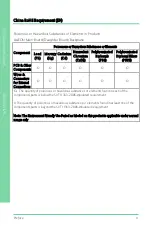
Summary of Contents for AAEON GENE-WHU6

Page 1: ...Last Updated October 27 2021 GENE WHU6 3 5 Subcompact Board User s Manual 5th Ed ...

Page 2: ...d in this manual is intended to be accurate and reliable However the original manufacturer assumes no responsibility for its use or for any infringements upon the rights of third parties that may result from its use The material in this document is for product information only and is subject to change without notice While reasonable efforts have been made in the preparation of this document to ass...

Page 3: ...gistered trademark of Microsoft Corp Intel and Celeron are registered trademarks of Intel Corporation Intel Core are trademarks of Intel Corporation ITE is a trademarkof Integrated Technology Express Inc IBM PC AT PS 2 and VGA are trademarks of International Business Machines Corporation All other product names or trademarks are properties oftheir respective owners ...

Page 4: ...g List Before setting up your product please make sure the following items have been shipped Item Quantity GENE WHU6 MB 1 Heatspreader 1 If any of these items are missing or damaged please contact your distributor or sales representative immediately ...

Page 5: ...d descriptions and explanations on the product s hardware and software features if any its specifications dimensions jumper connector settings definitions and driver installation instructions if any to facilitate users in setting up their product Users may refer to the product page at AAEON com for the latest version of this document ...

Page 6: ...transient over voltage 7 Always disconnect this device from any AC supply before cleaning 8 While cleaning use a damp cloth instead of liquid or spray detergents 9 Make sure the device is installed near a power outlet and is easily accessible 10 Keep this device away from humidity 11 Place the device on a solid surface during installation to prevent falls 12 Do not cover the openings on the device...

Page 7: ...usion to the device iii Exposure to moisture iv Device is not working as expected or in a manner as described in this manual v The device is dropped or damaged vi Any obvious signs of damage displayed on the device 18 DO NOT LEAVE THIS DEVICE IN AN UNCONTROLLED ENVIRONMENT WITH TEMPERATURES BEYOND THE DEVICE S PERMITTED STORAGE TEMPERATURES SEE CHAPTER 1 TO PREVENT DAMAGE ...

Page 8: ...plosion if the battery is incorrectly replaced Replace only with the same or equivalent type recommended by the manufacturer Dispose of used batteries according to the manufacturer s instructions and your local government s recycling or disposal directives Attention Il y a un risque d explosion si la batterie est remplacée de façon incorrecte Ne la remplacer qu avec le même modèle ou équivalent re...

Page 9: ...质或元素名称及含量 AAEON Main Board Daughter Board Backplane 部件名称 有毒有害物质或元素 铅 Pb 汞 Hg 镉 Cd 六价铬 Cr VI 多溴联苯 PBB 多溴二苯醚 PBDE 印刷电路板 及其电子组件 外部信号 连接器及线材 O 表示该有毒有害物质在该部件所有均质材料中的含量均在 SJ T 11363 2006 标准规定的限量要求以下 X 表示该有毒有害物质至少在该部件的某一均质材料中的含量超出 SJ T 11363 2006 标准规定的限量要求 备注 此产品所标示之环保使用期限 系指在一般正常使用状况下 ...

Page 10: ...henyl Ethers PBDE PCB Other Components O O O O O Wires Connectors for External Connections O O O O O O O The quantity of poisonous or hazardous substances or elements found in each of the component s parts is below the SJ T 11363 2006 stipulated requirement X The quantity of poisonous or hazardous substances or elements found in at least one of the component s parts is beyond the SJ T 11363 2006 s...

Page 11: ... JP4 11 2 3 4 LVDS eDP Port Backlight Lightness Control Mode Selection JP5 11 2 3 5 Touch Screen 4 5 8 Wire Selection JP8 11 2 3 6 Clear CMOS Jumper JP9 12 2 3 7 Auto Power Button Enable Disable Selection JP10 12 2 4 List of Connectors 13 2 4 1 5V Output for SATA HDD CN1 14 2 4 2 SATA Port CN2 15 2 4 3 External Power Input CN3 15 2 4 4 Audio I O Port CN5 16 2 4 5 External 5VSB Input CN6 17 2 4 6 D...

Page 12: ...21 31 2 4 21 CPU Fan CN22 33 2 4 22 Battery Connector CN23 34 2 4 23 LAN RJ 45 Port 1 Port 2 CN24 CN25 34 2 4 24 USB 3 2 Gen 2 Ports 0 1 CN26 35 2 4 25 USB 3 2 Gen 2 Ports 2 3 CN27 36 2 4 26 HDMI CN28 37 2 4 27 VGA Port CN29 38 2 4 28 M 2 B Key 2280 CN30 38 2 4 29 LAN SPD Connector CN31 39 2 5 Thermal Solutions 40 2 5 1 GENE WHU6 FAN01 40 2 5 2 GENE WHU6 FAN02 42 2 5 3 GENE WHU6 HSK01 44 2 5 4 GEN...

Page 13: ... 4 7 Digital IO Port Configuration 67 3 5 Setup Submenu Chipset 68 3 5 1 System Agent SA Configuration 69 3 5 1 1 LVDS Panel Configuration 70 3 5 2 PCH IO Configuration 73 3 5 2 1 Serial IO Configuration 74 3 6 Setup Submenu Security 75 3 6 1 Secure Boot 76 3 6 1 1 Key Management 77 3 7 Setup Submenu Boot 79 3 8 Setup Submenu Save Exit 80 Chapter 4 Driver Installation 81 4 1 Driver Download Instal...

Page 14: ...Preface XIV 3 5 Subcompact Board GENE WHU6 B 1 Mating Connectors and Cables 90 ...

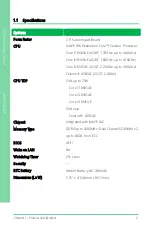
Page 15: ...3 5 Subcompact Board GENE WHU6 Chapter 1 Chapter 1 Product Specifications ...

Page 16: ... 8T 1 60GHz up to 4 10GHz Core i3 8145UE 2C 4T 2 20GHz up to 3 90GHz Celeron 4305UE 2C 2T 2 0GHz CPU TDP 15W up to 25W Core i7 8665UE Core i5 8365UE Core i3 8145UE 15W only Celeron 4305UE Chipset Integrated with Intel SoC Memory Type DDR4 up to 2400MHz Dual Channel SODIMM x 2 up to 64GB Non ECC BIOS UEFI Wake on LAN Y es Watchdog Timer 255 Level Security RTC Battery Lithium Battery3V 240mAh Dimens...

Page 17: ...t 12V with Intel i7 8665UE DDR4L 2400MHz 16GB memory Power Consumption Max 7 30A at 12V with Intel i7 8665UE DDR4L 2400MHz 16GB memory Display Controller Intel UHD Graphics 610 620 LVDS eDP LVDS Dual Channel 18 24 bit x 1 Optional eDP 1 4 Display Interface HDMI 2 0a x 1 VGA x 1 Multiple Display Support 3 Simultaneous Displays Audio Codec Realtek ALC897 892 Audio Interface Line in Line out MIC Spea...

Page 18: ... 485 supports 5V 12V RI Video LVDS eDP x 1 default LVDS SATA SATA III 6 0 Gbps x 1 5V SATA Power Connector x 1 Audio Audio Header x 1 DIO GPIO 8 bit SMBus I2C I2C SMBus x 1 Default I2C Touch 4 5 8 wire touch controller optional Fan DC Fan x 1 optional Smart Fan SIM Nano SIM x 1 Front Panel HDD LED PWR LED Power Button Buzzer Reset Others Expansion Mini PCIe mSATA Full Sized mSATA mPCIe x 1 mSATA a...

Page 19: ...6 Expansion M 2 Continued E Key M 2 2230 x 1 PCIe USB2 0 BIO Environmental Operating Temperature 32 F 140 F 0 C 60 C Storage Temperature 40 F 176 F 40 C 80 C Operating Humidity 0 90 relative humidity non condensing MTBF Hours 354 194 EMC Certification CE FCC Class A ...

Page 20: ...Chapter 1 Product Specifications 6 3 5 Subcompact Board GENE WHU6 1 2 Block Diagram ...

Page 21: ...3 5 Subcompact Board GENE WHU6 Chapter 2 Chapter 2 Hardware Information ...

Page 22: ...Chapter 2 Hardware Information 8 3 5 Subcompact Board GENE WHU6 2 1 Dimensions ...

Page 23: ...Chapter 2 Hardware Information 9 3 5 Subcompact Board GENE WHU6 2 2 Jumpers and Connectors ...

Page 24: ...LVDS eDP Port Backlight Inverter VCC Selection and Operating VDD Selection JP5 LVDS eDP Port Backlight Lightness Control Mode Selection JP8 Touch Screen 4 5 8 wire Mode Selection JP9 Clear CMOS Jumper JP10 Auto Power ButtonEnable Disable Selection 2 3 1 Front Panel Connector JP1 Pin Function Pin Function Pin 1 PWR_BTN Pin 2 PWR_BTN Pin 3 HDD_LED Pin 4 HDD_LED Pin 5 SPEAKER Pin 6 SPEAKER Pin 7 PWR_...

Page 25: ...ghtness Control Mode Selection JP5 VR Mode PWM Mode Default 2 3 5 Touch Screen 4 5 8 Wire Selection JP8 4 8 Wires Mode Default 5 Wires Mode 3 4 5 6 3 4 5 6 1 2 3 4 5 6 1 2 3 4 5 6 3 4 5 6 3 4 5 6 1 2 3 4 5 6 1 2 3 4 5 6 3 4 5 6 1 2 3 4 5 6 1 2 3 4 5 6 1 2 3 4 5 6 3 4 5 6 3 4 5 6 1 2 3 4 5 6 1 2 3 4 5 6 3 4 5 6 3 4 5 6 1 2 3 4 5 6 1 2 3 4 5 6 3 5 1 2 3 4 5 6 1 2 3 4 5 6 1 2 3 4 5 6 5 6 5 6 1 2 3 4 ...

Page 26: ...rdware Information 12 3 5 Subcompact Board GENE WHU6 2 3 6 Clear CMOS Jumper JP9 Normal Default Clear CMOS 2 3 7 Auto Power Button Enable Disable Selection JP10 Disable ATX Enable AT Default 1 2 3 1 2 3 1 2 3 1 2 3 ...

Page 27: ... CN5 Audio I O Port CN6 External 5VSB Input CN7 DDR4 SO DIMM Slot CN8 COM Port 1 RS 232 422 485 CN9 COM Port 2 RS 232 422 485 CN10 Mini Card Slot Full Size CN11 DDR4 SO DIMM Slot CN12 M 2 E Key 2230 CN13 LVDS eDP Port Inverter Backlight Connector CN14 LVDS eDP Port CN15 USB 2 0 Port 5 CN16 SPI Debug Port CN17 USB 2 0 Port 6 CN18 LPC Port CN19 Digital I O Port CN20 Nano SIM Card Socket CN21 Touch S...

Page 28: ...l Function CN25 LAN RJ 45 Port1 CN26 Dual USB3 1 Port 0 Port 1 CN27 Dual USB3 1 Port 2 Port 3 CN28 HDMI Connector CN29 VGA Port CN30 M 2 B Key 2280 CN31 LAN SDP CONN 2 4 1 5V Output for SATA HDD CN1 Pin Pin Name Signal Type Signal Level 1 5V PWR 5V at 1A 2 GND GND 5V GND ...

Page 29: ...l Type Signal Level 1 GND GND 2 SATA_TX DIFF 3 SATA_TX DIFF 4 GND GND 5 SATA_RX DIFF 6 SATA_RX DIFF 7 GND GND 2 4 3 External Power Input CN3 Pin Pin Name Signal Type Signal Level 1 12V PWR 9 36V or 12V at 8A 2 GND GND Note There are two types of power input 9 36V or 12V by BOM option Pin 1 Pin 7 12V GND ...

Page 30: ... CN5 Pin Pin Name Signal Type Signal Level 1 MIC_L IN 2 MIC_R IN 3 GND_AUDIO GND 4 LINE_L_IN IN 5 LINE_R_IN IN 6 GND_AUDIO GND 7 LEFT_OUT OUT 8 GND_AUDIO GND 9 RIGHT_OUT OUT 10 5V_AUDIO PWR 5V MIC_L 1 10 MIC_R LINE_L_IN LINE_R_IN LEFT_OUT RIGHT_OUT 5V_AUDIO GND_AUDIO GND_AUDIO GND_AUDIO ...

Page 31: ...mation 17 3 5 Subcompact Board GENE WHU6 2 4 5 External 5VSB Input CN6 Pin Pin Name Signal Type Signal Level 1 PS_ON OUT 5V 2 GND GND 3 5VSB PWR 5V at 2A 2 4 6 DDR SO DIMM Slot CN7 Standard Specifications 5VSB GND PS_ON 1 2 3 ...

Page 32: ...rmation 18 3 5 Subcompact Board GENE WHU6 2 4 7 COM Port 1 CN8 RS 232 Pin Pin Name Signal Type Signal Level 1 DCD1 IN 2 DSR1 IN 3 RX1 IN 4 RTS1 OUT 5V 5 TX1 OUT 5V 6 CTS1 IN 7 DTR1 OUT 5V 8 RI1 IN 9 GND GND 1 2 3 4 5 6 7 8 9 ...

Page 33: ...HU6 RS 485 Pin Pin Name Signal Type Signal Level 1 RS485_ D I O 5V 2 NC 3 RS485_D I O 5V 4 NC 5 NC 6 NC 7 NC 8 NC 9 GND GND RS 422 Pin Pin Name Signal Type Signal Level 1 RS422_TX OUT 5V 2 NC 3 RS422_TX OUT 5V 4 NC 5 RS422_RX IN 6 NC 7 RS422_RX IN 8 NC 9 GND GND ...

Page 34: ...rmation 20 3 5 Subcompact Board GENE WHU6 2 4 8 COM Port 2 CN9 RS 232 Pin Pin Name Signal Type Signal Level 1 DCD2 IN 2 DSR2 IN 3 RX2 IN 4 RTS2 OUT 5V 5 TX2 OUT 5V 6 CTS2 IN 7 DTR2 OUT 5V 8 RI2 IN 9 GND GND 1 2 3 4 5 6 7 8 9 ...

Page 35: ...4 NC 5 NC 6 NC 7 NC 8 NC 5V 12V PWR 5V 12V at 0 5A 9 GND GND RS 422 Pin Pin Name Signal Type Signal Level 1 RS422_TX2 OUT 5V 2 NC 3 RS422_TX2 OUT 5V 4 NC 5 RS422_RX2 IN 6 NC 7 RS422_RX2 IN 8 NC 5V 12V PWR 5V 12V at 0 5A 9 GND GND Note 1 COM2 RS 232 422 485 can be set by BIOS setting Default is RS 232 Note 2 Pin8 function can be set by JP3 See Ch 2 3 2 ...

Page 36: ...Level 1 PCIE_WAKE IN 2 3 3VSB PWR 3 3V 3 NC 4 GND GND 5 NC 6 1 5V PWR 1 5V 7 PCIE_CLK_REQ IN 8 UIM_PWR PWR 9 GND GND 10 UIM_DATA I O 11 PCIE_REF_CLK DIFF 12 UIM_CLK IN 13 PCIE_REF_CLK DIFF 14 UIM_RST IN 15 GND GND 16 UIM_VPP PWR 17 NC 18 GND GND 19 NC 20 W_DISABLE OUT 3 3V 21 GND GND 22 PCIE_RST OUT 3 3V 23 PCIE_RX DIFF 24 3 3VSB PWR 3 3V ...

Page 37: ...X DIFF 26 GND GND 27 GND GND 28 1 5V PWR 1 5V 29 GND GND 30 SMB_CLK I O 3 3V 31 PCIE_TX DIFF 32 SMB_DATA I O 3 3V 33 PCIE_TX DIFF 34 GND GND 35 GND GND 36 USB_D DIFF 37 GND GND 38 USB_D DIFF 39 3 3VSB PWR 3 3V 40 GND GND 41 3 3VSB PWR 3 3V 42 NC 43 GND GND 44 NC 45 NC 46 NC 47 NC 48 1 5V PWR 1 5V 49 NC 50 GND GND ...

Page 38: ...Standard Specifications 2 4 12 LVDS eDP Port Inverter Backlight Connector CN13 Pin Pin Name Signal Type Signal level 1 BKL_PWR PWR 5V 12V 2 BKL_CONTROL OUT 3 GND GND 4 GND GND 5 BKL_ENABLE OUT 3 3V Note 1 LVDS BKL_PWR can be set to 5V or 12V by JP4 See Ch 2 3 3 Note 2 LVDS BKL_PWR supports current of 1 5A Note 2 LVDS BKL_CONTROL can be set by JP5 See Ch 2 3 4 BLK_PWR 2 3 4 5 1 BKL_CONTROL GND GND ...

Page 39: ... current of 2A Pin LVDS eDP Signal Type Signal Level 1 BKL_ENABLE BKL_ENABLE OUT 2 BKL_CONTROL BKL_CONTROL OUT 3 LCD_PWR LCD_PWR PWR 3 3V 5V 4 GND GND GND 5 LVDS_A_CLK eDP_TXN3 DIFF 6 LVDS_A_CLK eDP_TXP3 DIFF 7 LCD_PWR LCD_PWR PWR 3 3V 5V 8 GND GND GND 9 LVDS_DA0 eDP_TXN2 DIFF 10 LVDS_DA0 eDP_TXP2 DIFF 11 LVDS_DA1 eDP_TXN1 DIFF 12 LVDS_DA1 eDP_TXP1 DIFF PIN 1 PIN 2 PIN 30 PIN 29 ...

Page 40: ... 15 LVDS_DA3 NC DIFF 16 LVDS_DA3 eDP_HPD DIFF 17 DDC_DATA eDP_AUX_N I O 3 3V 18 DDC_CLK eDP_AUX_P I O 3 3V 19 LVDS_DB0 NC DIFF 20 LVDS_DB0 NC DIFF 21 LVDS_DB1 NC DIFF 22 LVDS_DB1 NC DIFF 23 LVDS_DB2 NC DIFF 24 LVDS_DB2 NC DIFF 25 LVDS_DB3 NC DIFF 26 LVDS_DB3 NC DIFF 27 LCD_PWR LCD_PWR PWR 3 3V 5V 28 GND GND GND 29 LVDS_B_CLK NC DIFF 30 LVDS_B_CLK NC DIFF ...

Page 41: ... 2 0 Port 5 CN15 Pin Pin Name Signal Type Signal Level 1 5VSB PWR 5V at 0 5A 2 USB5_D DIFF 3 USB5_D DIFF 4 GND GND 5 GND GND 2 4 15 BIOS Debug Port CN16 Pin Pin Name Signal Type Signal Level 1 SPI_MISO OUT 2 GND GND 3 SPI_CLK IN P IN 1 P IN 2 P IN 3 P IN 4 P IN 5 P IN 6 P IN 7 ...

Page 42: ... 3 3VSB PWR 3 3V 5 SPI_MOSI IN 6 SPI_CS IN 7 NC 2 4 16 USB 2 0 Port 6 CN17 Pin Pin Name Signal Type Signal Level 1 5VSB PWR 5V at 0 5A 2 USB6_D DIFF 3 USB6_D DIFF 4 GND GND 5 G ND GND 2 4 17 LPC Port CN18 Pin Pin Name Signal Type Signal Level 1 LAD0 I O 3 3V 2 LAD1 I O 3 3V 3 LAD2 I O 3 3V 4 LAD3 I O 3 3V ...

Page 43: ... LFRAME IN 7 LRESET OUT 3 3V 8 GND GND 9 LCLK OUT 10 SMB_DATA I2C_SDA I O 11 SMB_CLK I2C_CLK OUT 12 SMB_ALERT SERIRQ IN 3 3V 2 4 18 Digital I O Port CN19 Pin Signal Description Pin Signal Description 1 PD0 2 PD1 3 PD2 4 PD3 5 PD4 6 PD5 7 PD6 8 PD7 9 V5S 0 5A 10 GND DIO1 DIO3 DIO5 DIO7 GND DIO0 1 2 9 10 DIO2 DIO4 DIO6 5V ...

Page 44: ...ardware Information 30 3 5 Subcompact Board GENE WHU6 2 4 19 Nano SIM Card Socket CN20 Pin Pin Name Signal Type Signal Level 1 UIM_PWR PWR 2 UIM_RST IN 3 UIM_CLK IN 4 NC 5 GND GND 6 UIM_VPP PWR 7 UIM_DATA I O 8 NC ...

Page 45: ...2 4 20 Touchscreen Connector Optional CN21 Note Touchmode can be set by BIOS 8 Wire Pin Pin Name Signal Type Signal Level 1 GND GND 2 TOP EXCITE IN 3 BOTTOM EXCITE IN 4 LEFT EXCITE IN 5 RIGHT EXCITE IN 6 TOP SENSE IN 7 BOTTOM SENSE IN 8 LEFT SENSE IN 9 RIGHT SENSE IN ...

Page 46: ...e Information 32 3 5 Subcompact Board GENE WHU6 4 Wire Pin Pin Name Signal Type Signal Level 1 GND GND 2 TOP IN 3 BOTTOM IN 4 LEFT IN 5 RIGHT IN 6 NC 7 NC 8 NC 9 NC 5 Wire Pin Pin Name Signal Type Signal Level 1 GND GND ...

Page 47: ... WHU6 5 Wire Pin Pin Name Signal Type Signal Level 2 UL Y IN 3 UR H IN 4 LL L IN 5 LR X IN 6 SENSE S IN 7 NC 8 NC 9 NC 2 4 21 CPU Fan CN22 Pin Pin Name Signal Type Signal Level 1 GND GND 2 FAN_POWER PWR 12V at 1A 3 FAN_TAC IN 4 NC Note Max driving current is 1A ...

Page 48: ...Connector CN23 Pin Pin Name Signal Type Signal level 1 3 3V PWR 3 3V 2 GND GND 2 4 23 L AN RJ 45 Port 1 Port 2 CN24 CN25 Pin Pin Name Signal Type Signal level 1 MDI0 DIFF 2 MDI0 DIFF 3 MDI1 DIFF 4 MDI2 DIFF 5 MDI2 DIFF 6 MDI1 DIFF 7 MDI3 DIFF 8 MDI3 DIFF 1 ACT LINK LED SPEED LED 8 ...

Page 49: ... 5VSB PWR 5V at 0 9A 2 USB0_D DIFF 3 USB0_D DIFF 4 GND GND 5 USB0_SSRX DIFF 6 USB0_SSRX DIFF 7 GND GND 8 USB0_SSTX DIFF 9 USB0_SSTX DIFF 10 5VSB PWR 5V at 0 9A 11 USB1_D DIFF 12 USB1_D DIFF 13 GND GND 14 USB1_SSRX DIFF 15 USB1_SSRX DIFF 16 GND GND 17 USB1_SSTX DIFF 18 USB1_SSTX DIFF 10 Port 1 Port 0 11 12 13 1 2 3 4 14 15 16 17 18 5 6 7 8 9 ...

Page 50: ...me Signal Type Signal Level 1 5VSB PWR 5V at 0 9A 2 USB2_D DIFF 3 USB2_D DIFF 4 GND GND 5 USB2_SSRX DIFF 6 USB2_SSRX DIFF 7 GND GND 8 USB2_SSTX DIFF 9 USB2_SSTX DIFF 10 5VSB PWR 5V at 0 9A 11 USB3_D DIFF 12 USB3_D DIFF 13 GND GND 14 USB3_SSRX DIFF 15 USB3_SSRX DIFF 16 GND GND 17 USB3_SSTX DIFF 18 USB3_SSTX DIFF ...

Page 51: ...in Name Signal Type Signal Level 1 HDMI_TX2 DIFF 2 GND GND 3 HDMI_TX2 DIFF 4 HDMI_TX1 DIFF 5 GND GND 6 HDMI_TX1 DIFF 7 HDMI_TX0 DIFF 8 GND GND 9 HDMI_TX0 DIFF 10 HDMI_CLK DIFF 11 GND GND 12 HDMI_CLK DIFF 13 NC 14 NC 15 DDC_CLK I O 5V 16 DDC_DATA I O 5V 17 GND GND 18 5V PWR 5V 19 HDMI_HPD ...

Page 52: ...Pin Name Signal Type Signal Level 1 RED OUT 2 GREEN OUT 3 BLUE OUT 4 NC 5 GND GND 6 RED_GND_RTN GND 7 GREEN_GND_RTN GND 8 BLUE_GND_RTN GND 9 5V PWR 5V 10 NC 11 NC 12 DDC_DATA I O 5V 13 HSYNC OUT 14 VSYNC OUT 15 DDC_CLK I O 5V 2 4 28 M 2 B Key 2280 CN30 Standard Specifications 1 6 10 11 15 5 ...

Page 53: ...Chapter 2 Hardware Information 39 3 5 Subcompact Board GENE WHU6 2 4 29 L AN SPD Connector CN31 Pin Pin Name Signal Type Signal Level 1 SDP0 I O 2 SDP1 I O 3 SDP2 I O 4 SDP3 I O ...

Page 54: ...Chapter 2 Hardware Information 40 3 5 Subcompact Board GENE WHU6 2 5 Thermal Solutions 2 5 1 GENE WHU6 FAN01 Single piece cooler does not require use of heat spreader ...

Page 55: ...Chapter 2 Hardware Information 41 3 5 Subcompact Board GENE WHU6 GENE WHU6 FAN01 Assembly ...

Page 56: ...Chapter 2 Hardware Information 42 3 5 Subcompact Board GENE WHU6 2 5 2 GENE WHU6 FAN02 Single piece cooler does not require use of heat spreader ...

Page 57: ...Chapter 2 Hardware Information 43 3 5 Subcompact Board GENE WHU6 GENE WHU6 FAN02 Assembly ...

Page 58: ...Chapter 2 Hardware Information 44 3 5 Subcompact Board GENE WHU6 2 5 3 GENE WHU6 HSK01 Singe piece heatsink does not require use of heat spreader Note Use only with Intel Core i3 and Celeron processors ...

Page 59: ...Chapter 2 Hardware Information 45 3 5 Subcompact Board GENE WHU6 GENE WHU6 HSK01 Assembly ...

Page 60: ...Chapter 2 Hardware Information 46 3 5 Subcompact Board GENE WHU6 2 5 4 GENE WHU6 HSK02 ...

Page 61: ...Chapter 2 Hardware Information 47 3 5 Subcompact Board GENE WHU6 Heat Spreader with Heatsink Cover ...

Page 62: ...Chapter 2 Hardware Information 48 3 5 Subcompact Board GENE WHU6 2 5 5 GENE WHU6 HSK03 Single piece heatsink does not require use of heat spreader Note Limited to use with less than 0 5 m s airflow ...

Page 63: ...Chapter 2 Hardware Information 49 3 5 Subcompact Board GENE WHU6 GENE WHU6 HSK03 Assembly ...

Page 64: ...3 5 Subcompact Board GENE WHU6 Chapter 3 Chapter 3 AMI BIOS Setup ...

Page 65: ...ration against the values stored in the CMOS memory and BIOS NVRAM If a system configuration is not found or an error is detected the module will load the default configuration and reboot automatically There are four situations in which you will need to setup system configuration 1 Y ou are starting your system for the first time 2 Y ou have changed the hardware attached to your system 3 The syste...

Page 66: ... turned off To enter BIOS Setup press Del or ESC immediately while your computer is powering up The function for each interface can be found below Main Date and time can be set here Press Tab to switch between date elements Advanced Access advanced hardware settings and Hardware Monitor Chipset Chipset settings and options Security Set admin and user passwords access secure boot options Boot Boot ...

Page 67: ...Chapter 3 AMI BIOS Setup 53 3 5 Subcompact Board GENE WHU6 3 3 Setup Submenu Main ...

Page 68: ...Chapter 3 AMI BIOS Setup 54 3 5 Subcompact Board GENE WHU6 3 4 Setup Submenu Advanced ...

Page 69: ...ce TCG EFI protocoland INT1A interface will not be available SHA 1 PCR Bank Disable Enable Optimal Default Failsafe Default Enable or Disable SHA 1 PCR Bank SHA256 PCR Bank Disable Enable Optimal Default Failsafe Default Enable or Disable SHA256 PCR Bank Pending Operation None Optimal Default Failsafe Default TPM Clear Schedule an Operation for the Security Device NOTE Y our Computer will reboot d...

Page 70: ...ement Hierarchy Disabled Enabled Optimal Default Failsafe Default Enable or Disable Endorsement Hierarchy TPM2 0 UEFI Spec Version TCG_1_2 TCG_2 Optimal Default Failsafe Default Select the TCG2 Spec Version Support TCG_1_2 Compatible mode for Win8 Win10 TCG_2 Support new TCG2 protocoland event format for Win10 or later Physical Presence Spec Version 1 2 1 3 Optimal Default Failsafe Default Select ...

Page 71: ...fe Default Number of cores to enable in each processor package Intel VMX Virtualization Technology Disabled Enabled Optimal Default Failsafe Default When enabled a VMM can utilize the additional hardware capabilities provided by Vanderpool Technology C States Disabled Enabled Optimal Default Failsafe Default Enable Disable C States Intel R SpeedStep tm Disabled Enabled Optimal Default Failsafe Def...

Page 72: ...Chapter 3 AMI BIOS Setup 58 3 5 Subcompact Board GENE WHU6 Options Summary Turbo Mode Disabled Enabled Optimal Default Failsafe Default Enable Disable Turbo mode ...

Page 73: ...abled Optimal Default Failsafe Default Enable Disable SATA Device SATA GEN SPEED Auto Optimal Default Failsafe Default GEN1 GEN2 GEN3 SATA GEN SPEED SELECTION mSATA port Disabled Enabled Optimal Default Failsafe Default Enable or Disable SATA Port Port Disabled Enabled Optimal Default Failsafe Default Enable or Disable SATA Port ...

Page 74: ...Chapter 3 AMI BIOS Setup 60 3 5 Subcompact Board GENE WHU6 3 4 4 Hardware Monitor Options Summary Smart Fan Disabled Enabled Optimal Default Failsafe Default Enable or Disable Smart Fan ...

Page 75: ... Linear fan application circuit to control 3 wire fan speed by fan s power terminal Output PWM mode open drain to control Intel 4 wire fans Fan 1 Smart Fan Control Manual Duty Mode Auto Cycle Mode Optimal Default Failsafe Default Smart Fan Mode Select Temperature Source CPU Temperature Optimal Default Failsafe Default System Temperature System Temperature 2 Select the monitored temperature source ...

Page 76: ...AMI BIOS Setup 62 3 5 Subcompact Board GENE WHU6 Manual Duty Mode Options Summary Manual Duty Mode 60 Optimal Default Failsafe Default Manual mode fan control user can write expected duty cycle PWM fan type 1 100 ...

Page 77: ...Chapter 3 AMI BIOS Setup 63 3 5 Subcompact Board GENE WHU6 3 4 5 SIO Configuration ...

Page 78: ...lt Failsafe Default Enable or Disable this Logical Device Possible Use Automatic Settings Optimal Default Failsafe Default IO 3F8h IRQ 4 IO 2F8h IRQ 3 Allows user to change Device s Resource settings New settings will be reflected on This Setup Page after System restarts Mode RS232 Optimal Default Failsafe Default RS422 RS485 UART RS232 422 485 selection ...

Page 79: ...lt Failsafe Default Enable or Disable this Logical Device Possible Use Automatic Settings Optimal Default Failsafe Default IO 2F8h IRQ 3 IO 3F8h IRQ 4 Allows user to change Device s Resource settings New settings will be reflected on This Setup Page after System restarts Mode RS232 Optimal Default Failsafe Default RS422 RS485 UART RS232 422 485 selection ...

Page 80: ...ate Optimal Default Failsafe Default Always On Always Off IO Restore AC power Loss RTC wake system from S5 Disable Optimal Default Failsafe Default Fixed Time Dynamic Time Fixed Time System will wake on the hr min sec specified n Dynamic Time System will wake on the current time Increase minute s Wake on LAN Enable Enabled Optimal Default Failsafe Default Disabled Enable Disable integrated LAN to ...

Page 81: ...rd GENE WHU6 3 4 7 Digital IO Port Configuration Options Summary GPI Output Input Set DIO as Input or Output GPO Output Input Set DIO as Input or Output Output Level High Optimal Default Failsafe Default Low Set output level when DIO pin is output ...

Page 82: ...Chapter 3 AMI BIOS Setup 68 3 5 Subcompact Board GENE WHU6 3 5 Setup Submenu Chipset ...

Page 83: ...Chapter 3 AMI BIOS Setup 69 3 5 Subcompact Board GENE WHU6 3 5 1 System Agent SA Configuration ...

Page 84: ...VDS Disabled Enabled Optimal Default Failsafe Default Enable Disable this panel LVDS Panel Type 640X480 60HZ 800X480 60HZ 800X600 60HZ 1024X600 60HZ 1024X768 60HZ Optimal Default Failsafe Default 1280X768 60HZ 1280X800 60HZ 1280X1024 60HZ 1366X768 60HZ 1440X900 60HZ 1600X1200 60HZ 1920X1080 60HZ 1920X1200 60HZ ...

Page 85: ...mal Optimal Default Failsafe Default Inverted Select backlight control signal type Backlight Level 0 10 20 30 40 50 60 70 80 Optimal Default Failsafe Default 90 100 Select backlight control level Backlight PWM Freq 100Hz 200Hz 220Hz Optimal Default Failsafe Default 500Hz 1 1KHz 2 2KHz 6 5KHz Select PWM frequency of backlight control signal Swing Level 150mV 200mV 250mV 300mV Optimal Default Failsa...

Page 86: ...Chapter 3 AMI BIOS Setup 72 3 5 Subcompact Board GENE WHU6 Options Summary Center Spreading Depth no spreading Optimal Default Failsafe Default 0 5 1 0 1 5 2 0 2 5 Select Center Spreading Depth ...

Page 87: ...IO Configuration Options Summary Full MiniCard Slot Function SATA Optimal Default Failsafe Default PCIe Select function enabled for Full MiniCard CN10 Slot M 2 KEY B Slot Function SATA PCIe Optimal Default Failsafe Default Select function enabled for M 2 KEY B CN30 Slot ...

Page 88: ...kipped PSF default will remain and device PCI CFG Space will still be visible This is needed to allow PCI enumerator access functions above 0 in a multifunction device The following devices depend on each other I2C0 and I2C1 2 3 UART0 and UART1 SPI0 1 UART2 and I2C4 5 UART 0 00 30 00 cannot be disabled when 1 Child device is enabled like CNVi Bluetooth _SB PCI0 UA00 BTH0 UART 0 00 30 00 cannot be ...

Page 89: ...hen the user enters the Setup utility A User Password does not provide access to many of the features in the Setup utility Select the password you wish to set and press Enter In the dialog box enter your password must be between 3 and 20 letters or numbers Press Enter and retype your password to confirm Press Enter again to set the password Removing the Password Select the password you want to rem...

Page 90: ...em is in User mode The mode change requires platform reset Secure Boot Mode Custom Optimal Default Failsafe Default Standard Secure Boot mode options Standard or Custom In Custom mode Secure Boot Policy variables can be configured by a physically present user without full authentication Restore Factory Keys Force System to User Mode Install factory default Secure Boot key databases Reset To Setup ...

Page 91: ...de change requires platform reset Restore Factory Keys Force System to User Mode Install factory default Secure Boot key databases Reset To Setup Mode Delete all Secure Boot key databases from NVRAM Export Secure Boot variables Copy NVRAM content of Secure Boot variables to files in a root folder on a file system device Enroll Efi Image Allow the image to run in Secure Boot mode Enroll SHA256 Hash...

Page 92: ... Delete Key Exchange Keys Details Export Update Append Delete Authorized Signatures Details Export Update Append Delete Forbidden Signatures Details Export Update Append Delete Authorized TimeStamps Update Append OsRecovery Signatures Update Append Enroll Factory Defaults or load certificates from a file 1 Public Key Certificate a EFI_SIGNATURE_LIST b EFI_CERT_X509 DER c EFI_CERT_RSA2048 bin d EFI...

Page 93: ...ENE WHU6 3 7 Setup Submenu Boot Options Summary Quiet Boot Disabled Enabled Optimal Default Failsafe Default Enable Disable showing boot logo Launch PXE ROM Disabled Optimal Default Failsafe Default Enabled Controls the execution of UEFI Network OpROM ...

Page 94: ...Chapter 3 AMI BIOS Setup 80 3 5 Subcompact Board GENE WHU6 3 8 Setup Submenu Save Exit ...

Page 95: ...3 5 Subcompact Board GENE WHU6 Chapter 4 Chapter 4 Driver Installation ...

Page 96: ...vers 1 Open the Step 1 Intel Chipset folder then the Win10 folder 2 Run the SetupChipset exe inthe folder 3 Follow the instructions 4 Drivers will be installed automatically Step 2 Install Graphics Drivers 1 Open the Step 2 Intel Graphics folder and select your OS 2 Run the igxpin exe file in the folder 3 Follow the instructions 4 Drivers will be installed automatically Step 3 Install ME Drivers 1...

Page 97: ...nd select your OS 2 Run the PROWinx64 exe file in the folder 3 Follow the instructions 4 Drivers will be installed automatically Step 6 Install Audio Driver 1 Open the Step 6 AUDIO folder and select your OS 2 Run the 0006 64bit_Win7_Win8_Win81_Win10_R279 exe file in the folder 3 Follow the instructions 4 Drivers will be installed automatically Step 7 Install Touch Driver 1 Open the Step 7 TOUCH fo...

Page 98: ...3 5 Subcompact Board GENE WHU6 Appendix A Appendix A I O Information ...

Page 99: ...Appendix A I O Information 85 3 5 Subcompact Board GENE WHU6 A 1 I O Address Map ...

Page 100: ...Appendix A I O Information 86 3 5 Subcompact Board GENE WHU6 A 2 Memory Address Map ...

Page 101: ...Appendix A I O Information 87 3 5 Subcompact Board GENE WHU6 A 3 IRQ Mapping Chart ...

Page 102: ...Appendix A I O Information 88 3 5 Subcompact Board GENE WHU6 ...

Page 103: ...3 5 Subcompact Board GENE WHU6 Appendix B Appendix B Mating Connectors and Cables ...

Page 104: ...o Connector Molex 51021 1000 Audio Cable 1709100254 CN6 External 5VSB Power Input and PS_ON JST PHR 3 ATX Cable 170220020B CN8 COM Port 1 Connector Molex 51021 0900 Serial Port Cable 1701090150 CN9 COM Port 2 Connector Molex 51021 0900 Serial Port Cable 1701090150 CN13 LVDS Inverter Connector JST PHR 5 N A N A CN14 LVDS Connector HIROSE DF13 30DS 1 25C N A N A CN15 USB Port Connector Molex 51021 0...

Page 105: ...l Function Mating Connector Available Cable Cable P N Vendor Model no CN19 Digital I O Connector Neltron 2026B 10 N A N A CN21 Touch Screen Connector JST SHR 9V S B N A N A CN22 CPU Fan Connector Molex 22 01 2035 N A N A CN23 External RTC Connector Molex 51021 0200 BatteryCable 175011901C ...

Reviews: