

SERVICE MANUAL
Sec. 1: Main Section
I
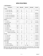
Specifications
I
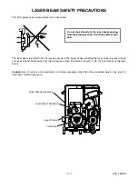
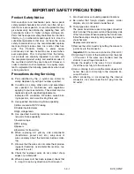
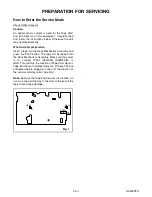
Preparation for Servicing
I
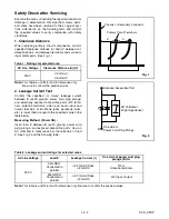
Adjustment Procedures
I
Schematic Diagrams
I
CBA’s
Sec. 2: Deck Mechanism Section
I
Standard Maintenance
I
Alignment for Mechanism
I
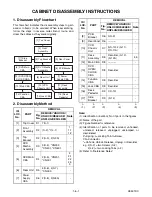
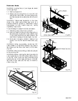
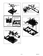
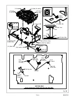
Disassembly/Assembly of Mechanism
I
Alignment Procedures of Mechanism
Sec. 3: Exploded views
and Parts List Section
I
Exploded views
I
Parts List
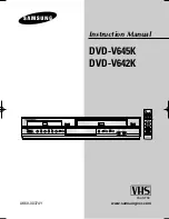
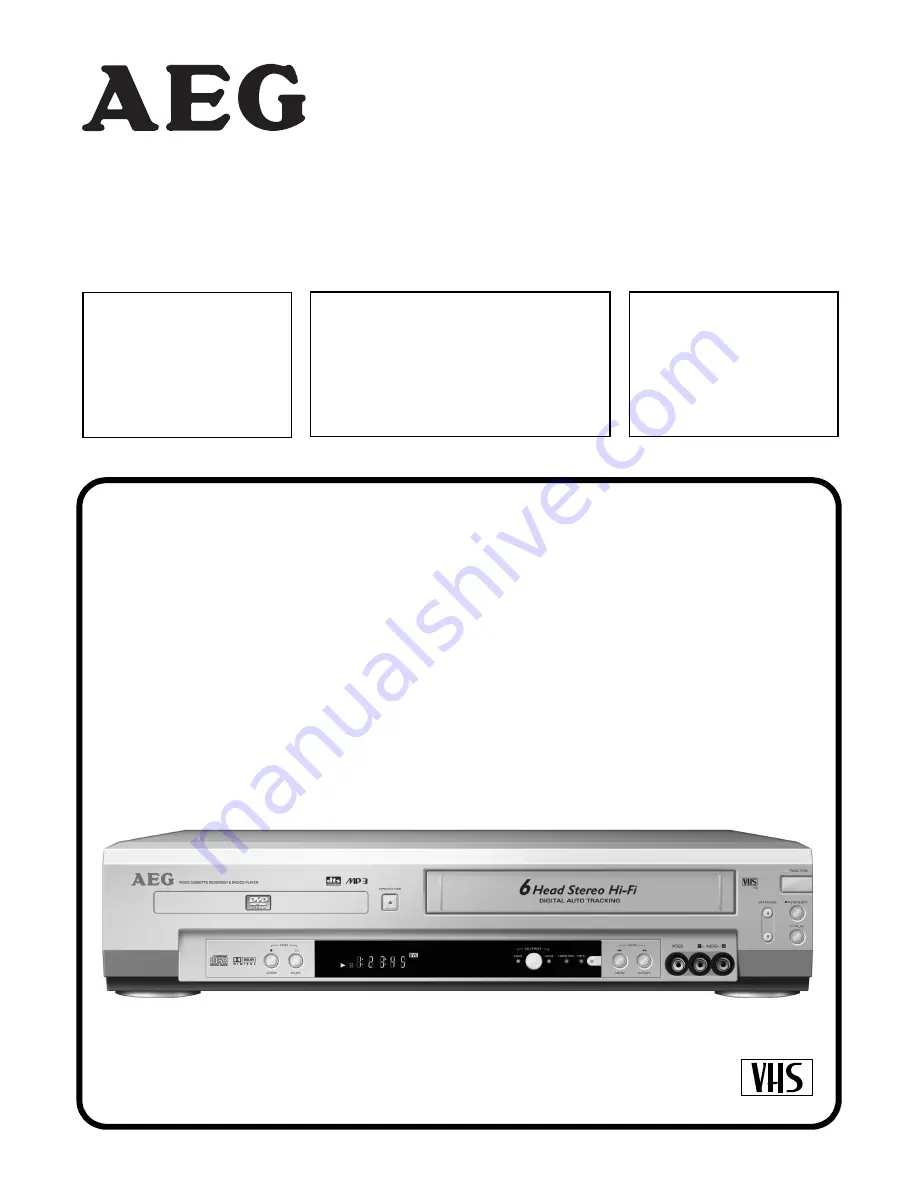
DVD PLAYER &
VIDEO CASSETTE RECORDER
VCR-D 4501
PA L
Summary of Contents for VCR-D 4501
Page 30: ...Main 1 9 Schematic Diagram VCR Section 1 10 3 1 10 4 H9504SCM1 ...
Page 32: ...1 10 7 1 10 8 H9504SCM3 Main 3 9 Schematic Diagram VCR Section ...
Page 33: ...Main 4 9 Schematic Diagram VCR Section 1 10 9 1 10 10 H9504SCM4 ...
Page 34: ...Main 5 9 Schematic Diagram VCR Section 1 10 11 1 10 12 H9504SCM5 ...
Page 35: ...Main 6 9 Schematic Diagram VCR Section 1 10 13 1 10 14 H9504SCM6 ...
Page 36: ...Main 7 9 Schematic Diagram VCR Section 1 10 15 1 10 16 H9504SCM7 ...
Page 37: ...Main 8 9 DVD Open Close Schematic Diagram VCR Section 1 10 17 1 10 18 H9504SCM8 ...
Page 38: ...1 10 19 1 10 20 Main 9 9 Schematic Diagram VCR Section H9504SCM9 ...
Page 40: ...1 10 23 1 10 24 Jack Schematic Diagram VCR Section H9504SCJ ...
Page 41: ...1 10 25 1 10 26 Function Schematic Diagram VCR Section H9504SCF ...
Page 42: ...1 10 27 1 10 28 AFV Schematic Diagram VCR Section H9504SCAFV ...
Page 44: ...1 10 31 Main CBA Bottom View BH9510F01014A 1 10 32 ...
Page 48: ...DVD Main 1 3 Schematic Diagram DVD Section H9504SCD1 1 10 39 1 10 40 ...
Page 49: ...1 10 41 1 10 42 DVD Main 2 3 Schematic Diagram DVD Section H9504SCD2 ...
Page 51: ...DVD Main 3 3 Schematic Diagram DVD Section 1 10 45 1 10 46 H9504SCD3 ...
Page 98: ...VCR D 4501 H9504ED 2004 04 01 ...