background image

Relion

®

 670 series

Line differential protection RED670 ANSI

Technical reference manual

Summary of Contents for Relion 670 series

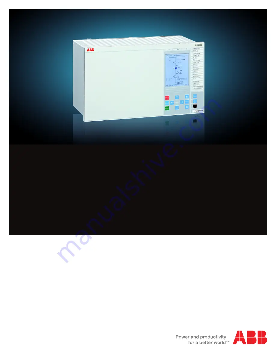
Page 1: ...Relion 670 series Line differential protection RED670 ANSI Technical reference manual...

Page 2: ......

Page 3: ...Document ID 1MRK505222 UUS Issued February 2015 Revision C Product version 1 2 Copyright 2012 ABB All rights reserved...

Page 4: ...n are registered trademarks of the ABB Group All other brand or product names mentioned in this document may be trademarks or registered trademarks of their respective holders Warranty Please inquire...

Page 5: ...roduct failure would create a risk for harm to property or persons including but not limited to personal injuries or death shall be the sole responsibility of the person or entity applying the equipme...

Page 6: ...ectrical equipment for use within specified voltage limits Low voltage directive 2006 95 EC This conformity is the result of tests conducted by ABB in accordance with the product standards EN 50263 an...

Page 7: ...Technical data 42 Intended audience 42 Related documents 42 Revision notes 43 Section 2 Analog inputs 45 Introduction 45 Operation principle 45 Function block 46 Setting parameters 47 Section 3 Local...

Page 8: ...n time model 82 Function block 83 Output signals 83 Setting parameters 83 Technical data 83 Time synchronization 84 Introduction 84 Principle of operation 84 General concepts 84 Real time clock RTC op...

Page 9: ...l matrix for binary inputs SMBI 104 Introduction 104 Principle of operation 105 Function block 105 Input and output signals 105 Signal matrix for binary outputs SMBO 106 Introduction 106 Principle of...

Page 10: ...2 Line differential protection 3 or 6 CT sets L3CPDIF L6CPDIF 122 Line differential protection 3 or 6 CT sets with in zone transformers LT3CPDIF LT6CPDIF 124 Analog signal transfer for line differenti...

Page 11: ...tification 173 Introduction 21 173 Principle of operation 174 Full scheme measurement 174 Impedance characteristic 175 Minimum operating current 179 Measuring principles 180 Directional impedance elem...

Page 12: ...n block 236 Input and output signals 236 Setting parameters 237 Technical data 239 Full scheme distance measuring Mho characteristic ZMHPDIS 21 239 Introduction 239 Principle of operation 241 Full sch...

Page 13: ...DIR 280 Function block 282 Input and output signals 283 Setting parameters 284 Mho impedance supervision logic ZSMGAPC 285 Introduction 285 Principle of operation 285 Fault inception detection 285 Fun...

Page 14: ...hment 333 Minimum operate currents 338 Simplified logic diagrams 339 Function block 344 Input and output signals 344 Setting parameters 345 Technical data 346 Power swing detection ZMRPSB 68 347 Intro...

Page 15: ...etting parameters 371 Technical data 372 Phase preference logic PPLPHIZ 372 Introduction 372 Principle of operation 373 Function block 375 Input and output signals 376 Setting parameters 376 Section 7...

Page 16: ...404 Directional supervision element with integrated directional comparison function 405 Second harmonic blocking element 408 Switch on to fault feature 410 Function block 413 Input and output signals...

Page 17: ...etting parameters 455 Technical data 456 Breaker failure protection CCRBRF 50BF 456 Introduction 457 Operation principle 457 Function block 460 Input and output signals 460 Setting parameters 461 Tech...

Page 18: ...f analog inputs 482 Function block 484 Input and output signals 484 Setting parameters 485 Technical data 486 Broken conductor check BRCPTOC 46 486 Introduction 486 Principle of operation 487 Function...

Page 19: ...n block 525 Input and output signals 526 Setting parameters 526 Technical data 528 Overexcitation protection OEXPVPH 24 529 Introduction 529 Principle of operation 529 Measured voltage 532 Operate tim...

Page 20: ...age dependent time delay 553 Blocking 554 Design 554 Function block 555 Input and output signals 555 Setting parameters 556 Technical data 557 Overfrequency protection SAPTOF 81 557 Introduction 558 P...

Page 21: ...577 Logic diagram 577 Function block 583 Input and output signals 584 Setting parameters 585 Technical data 593 Section 11 Secondary system supervision 597 Current circuit supervision CCSRDIF 87 597 I...

Page 22: ...n 634 Initiate auto reclosing and conditions for initiation of a reclosing cycle 634 Control of the auto reclosing open time for shot 1 636 Long trip signal 637 Time sequence diagrams 643 Function blo...

Page 23: ...n 675 Principle of operation 676 Function block 680 Input and output signals 680 Setting parameters 681 Bay reserve QCRSV 681 Introduction 681 Principle of operation 682 Function block 684 Input and o...

Page 24: ...or bus coupler bay ABC_BC 3 704 Introduction 705 Function block 706 Logic diagram 707 Input and output signals 709 Interlocking for breaker and a half diameter BH 3 712 Introduction 712 Function block...

Page 25: ...760 Function block 761 Input and output signals 762 Setting parameters 762 IEC61850 generic communication I O functions DPGGIO 762 Introduction 763 Principle of operation 763 Function block 763 Input...

Page 26: ...and output signals 794 Setting parameters 795 Technical data 795 Phase segregated scheme communication logic for distance protection ZC1PPSCH 85 796 Introduction 796 Principle of operation 796 Blockin...

Page 27: ...Unblocking scheme 815 Function block 816 Input and output signals 816 Setting parameters 817 Technical data 817 Current reversal and weak end infeed logic for residual overcurrent protection ECRWPSCH...

Page 28: ...block 837 Input and output signals 837 Setting parameters 838 Technical data 839 Sudden change in current variation SCCVPTOC 51 839 Introduction 840 Principle of operation 840 Function block 841 Input...

Page 29: ...quence overcurrent protection LCZSPTOC 51N 850 Introduction 851 Principle of operation 851 Function block 851 Input and output signals 851 Setting parameters 852 Technical data 852 Three phase overcur...

Page 30: ...5 Exclusive OR function block XOR 876 Loop delay function block LOOPDELAY 876 Set reset with memory function block SRMEMORY 877 Reset set with memory function block RSMEMORY 878 Controllable gate func...

Page 31: ...output signals 893 Setting parameters 894 Section 15 Monitoring 895 Measurements 895 Introduction 896 Principle of operation 897 Measurement supervision 897 Measurements CVMMXN 901 Phase current measu...

Page 32: ...40 Measuring Principle 940 Accurate algorithm for measurement of distance to fault 941 The non compensated impedance model 945 IEC 60870 5 103 945 Function block 945 Input and output signals 946 Setti...

Page 33: ...6 Introduction 976 Principle of operation 976 Function block 977 Input signals 977 Technical data 977 Disturbance recorder 977 Introduction 977 Principle of operation 978 Memory and storage 979 IEC 60...

Page 34: ...995 Setting parameters 996 IEC 61850 generic communication I O functions MVGGIO 996 Principle of operation 996 Function block 996 Input and output signals 997 Setting parameters 997 IEC 61850 8 1 red...

Page 35: ...47 Function block 1047 Input and output signals 1050 Setting parameters 1055 Technical data 1058 Horizontal communication via GOOSE for interlocking GOOSEINTLKRCV 1059 Function block 1059 Input and ou...

Page 36: ...ware modules 1085 Overview 1085 Combined backplane module CBM 1086 Introduction 1086 Functionality 1087 Design 1087 Universal backplane module UBM 1089 Introduction 1089 Functionality 1089 Design 1089...

Page 37: ...112 mA input module MIM 1114 Introduction 1114 Design 1115 Technical data 1116 Serial and LON communication module SLM 1117 Introduction 1117 Design 1117 Technical data 1118 Galvanic RS485 communicati...

Page 38: ...Wall mounting dimensions 1142 External resistor unit for high impedance differential protection 1142 Mounting alternatives 1144 Flush mounting 1144 Overview 1144 Mounting procedure for flush mounting...

Page 39: ...154 Type tests according to standard 1155 Section 20 Labels 1159 Labels on IED 1159 Section 21 Connection diagrams 1163 Section 22 Inverse time characteristics 1179 Application 1179 Principle of opera...

Page 40: ...34...

Page 41: ...al Engineering Installing Commissioning Operation Maintenance Decommissioning deinstalling Application manual Operator s manual Installation and Engineeringmanual Commissioning manual manual Technical...

Page 42: ...n how to engineer the IEDs using the different tools in PCM600 The manual provides instructions on how to set up a PCM600 project and insert IEDs to the project structure The manual also recommends a...

Page 43: ...bes binary and analog signal transfer and the associated hardware Hardware describes the IED and its components Connection diagrams provides terminal wiring diagrams and information regarding connecti...

Page 44: ...nfigured using the ACT tool They can be connected to the inputs and outputs of other functions and to binary inputs and outputs Examples of input signals are BLKTR BLOCK and VTSU Examples output signa...

Page 45: ...int BLOCK int BLOCK int OR AND AND AND OR AND 0 ANSI04000375 V1 EN Figure 1 Logic diagram example with int signals External signals Signal paths that extend beyond the logic diagram and continue in a...

Page 46: ...ANSI04000376 V1 EN Figure 2 Logic diagram example with an outgoing cont signal or or or AND AND AND AND BLK cont PICKUP PU_C PU_B PU_A 15 ms 0 15 ms 0 15 ms 0 15 ms 0 or STND_AG cont STND_BG cont STND...

Page 47: ...be found in the signal list but described in the settings table The character in front of an input or output signal name in the function block symbol given for a function indicates that the user can...

Page 48: ...d functional logics in the protective devices The installation and commissioning personnel must have a basic knowledge in the handling electronic equipment 1 1 5 Related documents Documents related to...

Page 49: ...et up for Relion 670 series 1MRK 505 260 UEN More information can be found on www abb com substationautomation 1 1 6 Revision notes Revision Description A Minor corrections made B Maintenance updates...

Page 50: ...44...

Page 51: ...n in relation to this analog input During testing and commissioning of the IED the reference channel can be changed to facilitate testing and service values reading The availability of VT inputs depen...

Page 52: ...dition then a positive quantity always flows towards the protected object and a Forward direction always looks towards the protected object The settings of the IED is performed in primary values The r...

Page 53: ...40 Ch10 TRM40 Ch11 TRM40 Ch12 TRM41 Ch1 TRM41 Ch2 TRM41 Ch3 TRM41 Ch4 TRM41 Ch5 TRM41 Ch6 TRM41 Ch7 TRM41 Ch8 TRM41 Ch9 TRM41 Ch10 TRM41 Ch11 TRM41 Ch12 MU1 IA MU1 IB MU1 IC MU1 I0 MU1 VA MU1 VB MU1 V...

Page 54: ...FromObject the opposite CTsec5 1 10 A 1 1 Rated CT secondary current CTprim5 1 99999 A 1 3000 Rated CT primary current CT_WyePoint6 FromObject ToObject ToObject ToObject towards protected object FromO...

Page 55: ...ent CTprim2 1 99999 A 1 3000 Rated CT primary current CT_WyePoint3 FromObject ToObject ToObject ToObject towards protected object FromObject the opposite CTsec3 1 10 A 1 1 Rated CT secondary current C...

Page 56: ...Rated CT primary current CT_WyePoint2 FromObject ToObject ToObject ToObject towards protected object FromObject the opposite CTsec2 1 10 A 1 1 Rated CT secondary current CTprim2 1 99999 A 1 3000 Rate...

Page 57: ...10 A 1 1 Rated CT secondary current CTprim5 1 99999 A 1 3000 Rated CT primary current CT_WyePoint6 FromObject ToObject ToObject ToObject towards protected object FromObject the opposite CTsec6 1 10 A...

Page 58: ...e CTsec5 1 10 A 1 1 Rated CT secondary current CTprim5 1 99999 A 1 3000 Rated CT primary current CT_WyePoint6 FromObject ToObject ToObject ToObject towards protected object FromObject the opposite CTs...

Page 59: ...11 0 05 2000 00 kV 0 05 400 00 Rated VT primary voltage VTsec12 0 001 999 999 V 0 001 110 000 Rated VT secondary voltage VTprim12 0 05 2000 00 kV 0 05 400 00 Rated VT primary voltage 1MRK505222 UUS C...

Page 60: ...54...

Page 61: ...n the product capability The local HMI is divided into zones with different functionality Status indication LEDs Alarm indication LEDs which consist of 15 LEDs 6 red and 9 yellow with user printable l...

Page 62: ...me LCD which measures 4 7 x 3 5 inches It has 28 lines with up to 40 characters per line To display the single line diagram this LCD is required 3 2 2 Design The different parts of the medium size loc...

Page 63: ...igure 7 Medium size graphic HMI 1 Status indication LEDs 2 LCD 3 Indication LEDs 4 Label 5 Local Remote LEDs 6 RJ45 port 7 Communication indication LED 8 Keypad 1MRK505222 UUS C Section 3 Local HMI 57...

Page 64: ...able 7 HMI keys on the front of the IED Key Function IEC06000532 V1 EN Press to close or energize a breaker or disconnector IEC06000533 V1 EN Press to open a breaker or disconnector IEC05000103 V1 EN...

Page 65: ...nd in the menu tree IEC05000112 V1 EN Press to move down in the single line diagram and in the menu tree 3 4 LED 3 4 1 Introduction The LED module is a unidirectional means of communicating This means...

Page 66: ...ndicates normal operation Flashing light indicates alarm Alarm LEDs can be configured in PCM600 and depend on the binary logic Therefore they can not be configured on the local HMI Typical examples of...

Page 67: ...auto repeat On or not Off ContrastLevel 10 20 1 0 Contrast level for display DefaultScreen 0 0 1 0 Default screen EvListSrtOrder Latest on top Oldest on top Latest on top Sort order of event list Sym...

Page 68: ...n the LCD HMI is steady YELLOW F BOOLEAN Yellow LED on the LCD HMI is flashing RSTPULSE BOOLEAN A reset pulse is provided when the LEDs on the LCD HMI are cleared LEDSRST BOOLEAN Active when the LEDs...

Page 69: ...EDs which are used in collecting mode of operation are accumulated continuously until the unit is acknowledged manually This mode is suitable when the LEDs are used as a simplified alarm system Re sta...

Page 70: ...dy light Operating sequences The operating sequences can be of type Follow or Latched For the Follow type the LED follows the input signal completely For the Latched type each LED latches to the corre...

Page 71: ...uence is the same as sequence 1 Follow S but the LEDs are flashing instead of showing steady light Sequence 3 LatchedAck F S This sequence has a latched function and works in collecting mode Every LED...

Page 72: ...new disturbance when activating any input signal for other LEDs set to sequence 6 LatchedReset S Also in this case indications that are still activated will not be affected by manual reset that is imm...

Page 73: ...d with a timer tMax after which time the influence on the definition of a disturbance of that specific LED is inhibited This functionality is shown i diagram in figure 15 Activating signal AND To dist...

Page 74: ...eset LED 1 Disturbance tRestart IEC01000239 V2 EN Figure 16 Operating sequence 6 LatchedReset S two indications within same disturbance Figure 17 shows the timing diagram for a new indication after tR...

Page 75: ...tRestart Disturbance tRestart IEC01000240 V2 EN Figure 17 Operating sequence 6 LatchedReset S two different disturbances Figure 18 shows the timing diagram when a new indication appears after the firs...

Page 76: ...LED 1 Disturbance tRestart IEC01000241 V2 EN Figure 18 Operating sequence 6 LatchedReset S two indications within same disturbance but with reset of activating signal between Figure 19 shows the timi...

Page 77: ...en vsd LEDGEN BLOCK RESET LEDTEST NEWIND ACK IEC05000508 V2 EN Figure 20 LEDGEN function block 3 5 4 4 Input and output signals Table 11 LEDGEN Input signals Name Type Default Description BLOCK BOOLEA...

Page 78: ...SeqTypeLED1 Follow S Follow F LatchedAck F S LatchedAck S F LatchedColl S LatchedReset S Follow S Sequence type for LED 1 SeqTypeLED2 Follow S Follow F LatchedAck F S LatchedAck S F LatchedColl S Latc...

Page 79: ...e for LED 8 SeqTypeLED9 Follow S Follow F LatchedAck F S LatchedAck S F LatchedColl S LatchedReset S Follow S Sequence type for LED 9 SeqTypeLED10 Follow S Follow F LatchedAck F S LatchedAck S F Latch...

Page 80: ...w S Sequence type for LED 13 SeqTypeLED14 Follow S Follow F LatchedAck F S LatchedAck S F LatchedColl S LatchedReset S Follow S Sequence type for LED 14 SeqTypeLED15 Follow S Follow F LatchedAck F S L...

Page 81: ...IED and the PCM600 is implemented at both access points to the IED local through the local HMI remote through the communication ports 4 1 1 Principle of operation There are different levels or types...

Page 82: ...tion possibilities application configuration including SMT GDE and CMT R R W R R R R W R W File loading database loading from XML file R W R W R W File dumping database dumping to XML file R W R W R W...

Page 83: ...o the IED then when a user intentionally attempts a Log on or when the user attempts to perform an operation that is password protected the Log on window will appear The cursor is focused on the User...

Page 84: ...from the Event Viewer in PCM600 or from a SMS SCS system Under the Diagnostics menu in the local HMI the present information from the self supervision function can be reviewed The information can be...

Page 85: ...r IO fail IO stopped IO started OR Set Reset OR e g IOM2 Error e g IO n Error OR OR Internal FAIL Set Reset LON ERROR Watchdog RTE fatal error RTE Appl fail RTE OK IEC61850 not ready RTCERROR FTF fata...

Page 86: ...are also called internal signals The internal signals can be divided into two groups Standard signals are always presented in the IED see Table 15 Hardware dependent internal signals are collected dep...

Page 87: ...ernal signals are active RTCERROR IEC61850ERROR RTCERROR This signal will be active when there is a hardware error with the real time clock TIMESYNCHERROR This signal will be active when the source of...

Page 88: ...the analog input signal into two A D converter s with different amplification makes it possible to supervise the A D converters under normal conditions where the signals from the two A D converters sh...

Page 89: ...SIG function block 4 2 4 Output signals Table 18 INTERRSIG Output signals Name Type Description FAIL BOOLEAN Internal fail WARNING BOOLEAN Internal warning CPUFAIL BOOLEAN CPU fail CPUWARN BOOLEAN CPU...

Page 90: ...ation 4 3 2 1 General concepts Time definitions The error of a clock is the difference between the actual time of the clock and the time the clock is intended to have Clock accuracy indicates the incr...

Page 91: ...en it reaches the event recorder Thus the hardware clock can run independently The echo mode for the differential protection is based on the hardware clock Thus there is no need to synchronize the har...

Page 92: ...tting Slow clock synchronization mode During normal service a setting with slow synchronization mode is normally used which prevents the hardware clock to make too big time steps 16 s emanating from t...

Page 93: ...nfigured as fine If the synchronization message which is similar to the other messages has an offset compared to the internal time in the IED the message is used directly for synchronization that is f...

Page 94: ...ssage is sent from an IED to an SNTP server and the SNTP server returns the message after filling in a reception time and a transmission time SNTP operates via the normal Ethernet network that connect...

Page 95: ...minute pulse is connected to any channel on any Binary Input Module in the IED The electrical characteristic is thereby the same as for any other binary input If the objective of synchronization is t...

Page 96: ...reafter The definition of a minute pulse is that it occurs one minute after the previous minute pulse so the first minute pulse is not used at all The second minute pulse will probably be rejected due...

Page 97: ...IRIG B contains information of the year If x is 0 1 2 or 3 the information contains only the time within the year and year information has to come from PCM600 or local HMI The IRIG B module also take...

Page 98: ...ed Coarse time synchronization source FineSyncSource Disabled SPA LON BIN GPS GPS SPA GPS LON GPS BIN SNTP GPS SNTP IRIG B GPS IRIG B PPS Disabled Fine time synchronization source SyncMaster Disabled...

Page 99: ...ress RedServIP Add 0 18 IP Address 1 0 0 0 0 Redundant server IP address Table 24 DSTBEGIN Non group settings basic Name Values Range Unit Step Default Description MonthInYear January February March A...

Page 100: ...ime ends UTCTimeOfDay 0 172800 s 1 3600 UTC Time of day in seconds when daylight time ends Table 26 TIMEZONE Non group settings basic Name Values Range Unit Step Default Description NoHalfHourUTC 24 2...

Page 101: ...ve setting group Seven functional output signals are available for configuration purposes so that up to date information on the active setting group is always available A setting group is selected by...

Page 102: ...above example also includes seven output signals for confirmation of which group that is active SETGRPS function block has an input where the number of setting groups used is defined Switching can onl...

Page 103: ...CTGRP6 BOOLEAN 0 Selects setting group 6 as active Table 30 ActiveGroup Output signals Name Type Description GRP1 BOOLEAN Setting group 1 is active GRP2 BOOLEAN Setting group 2 is active GRP3 BOOLEAN...

Page 104: ...nadvertent IED configuration changes beyond a certain point in time 4 5 2 Principle of operation The Change lock function CHNGLCK is configured using ACT The function when activated will still allow t...

Page 105: ...eration LockHMI and Com LockHMI EnableCom EnableHMI LockCom LockHMI and Com Operation mode of change lock 4 6 Test mode functionality TEST 4 6 1 Introduction When the Test mode functionality TESTMODE...

Page 106: ...nable these blockings the IED must be set in test mode output ACTIVE is activated see example in figure 33 When leaving the test mode that is entering normal mode these blockings are disabled and ever...

Page 107: ...ocked from sending events over IEC 61850 station bus to prevent filling station and SCADA databases with test events for example during a maintenance test Time V Normal voltage Pickup1 Pickup2 IntBlkS...

Page 108: ...e OUTPUT BOOLEAN Test input is active SETTING BOOLEAN Test mode setting is Enabled or not Disabled NOEVENT BOOLEAN Event disabled during testmode 4 6 5 Setting parameters Table 37 TESTMODE Non group s...

Page 109: ...StationNumber 0 99999 1 0 Station number ObjectName 0 18 1 Object name Object name ObjectNumber 0 99999 1 0 Object number UnitName 0 18 1 Unit name Unit name UnitNumber 0 99999 1 0 Unit number 4 8 Pro...

Page 110: ...entifiers are available IEDProdType Describes the type of the IED like REL REC or RET Example REL670 FirmwareVer Describes the firmware version Example 1 4 51 Firmware versions numbers are running ind...

Page 111: ...ion The input output user defined name will also appear on the respective output input signal 4 9 3 Function block IEC05000434 2 en vsd SMBI VIN1 VIN2 VIN3 VIN4 VIN5 VIN6 VIN7 VIN8 VIN9 VIN10 BI1 BI2...

Page 112: ...D configuration 4 10 2 Principle of operation The Signal matrix for binary outputs SMBO function see figure 36 receives logical signal from the IED configuration which is transferring to the real hard...

Page 113: ...e for BO5 in Signal Matrix Tool BO6 BOOLEAN 1 Signal name for BO6 in Signal Matrix Tool BO7 BOOLEAN 1 Signal name for BO7 in Signal Matrix Tool BO8 BOOLEAN 1 Signal name for BO8 in Signal Matrix Tool...

Page 114: ...440 2 en vsd SMMI VIN1 VIN2 VIN3 VIN4 VIN5 VIN6 AI1 AI2 AI3 AI4 AI5 AI6 IEC05000440 V2 EN Figure 37 SMMI function block 4 11 4 Input and output signals Table 42 SMMI Input signals Name Type Default De...

Page 115: ...neutral value either voltage or current see figure 39 and figure 40 SMAI outputs give information about every aspect of the 3ph analog signals acquired phase angle RMS value frequency and frequency d...

Page 116: ...ample The above described scenario does not work if SMAI setting ConnectionType is Ph N If only one phase ground voltage is available the same type of connection can be used but the SMAI ConnectionTyp...

Page 117: ...t signals Table 44 SMAI1 Input signals Name Type Default Description BLOCK BOOLEAN 0 Block group 1 DFTSPFC REAL 20 0 Number of samples per fundamental cycle used for DFT calculation GRP1_A STRING Samp...

Page 118: ...nput to be used for group 2 phase B calculations GRP2_C STRING Sample input to be used for group 2 phase C calculations GRP2_N STRING Sample input to be used for group 2 residual calculations Table 47...

Page 119: ...DFTRefCh4 AdDFTRefCh5 AdDFTRefCh6 AdDFTRefCh7 AdDFTRefCh8 AdDFTRefCh9 AdDFTRefCh10 AdDFTRefCh11 AdDFTRefCh12 External DFT ref InternalDFTRef DFT reference ConnectionType Ph N Ph Ph Ph N Input connecti...

Page 120: ...Disabled NegateN Negate3Ph Negate3Ph N Disabled Negation MinValFreqMeas 5 200 1 10 Limit for frequency calculation in of VBase VBase 0 05 2000 00 kV 0 05 400 00 Base voltage 4 13 Summation block 3 pha...

Page 121: ...Group 1 analog input 3 phase group G2AI3P GROUP SIGNAL Group 2 analog input 3 phase group Table 53 3PHSUM Output signals Name Type Description AI3P GROUP SIGNAL Group analog input 3 phase group AI1 GR...

Page 122: ...Introduction Authority status ATHSTAT function is an indication function block for user log on activity 4 14 2 Principle of operation Authority status ATHSTAT function informs about two events relate...

Page 123: ...mit overload on the IED produced by heavy Ethernet network traffic The communication facilities must not be allowed to compromise the primary functionality of the device All inbound network traffic wi...

Page 124: ...AB LINKUP WARNING ALARM IEC09000750 1 en vsd IEC09000750 V1 EN Figure 44 DOSOEMAB function block DOSOEMCD LINKUP WARNING ALARM IEC09000751 1 en vsd IEC09000751 V1 EN Figure 45 DOSOEMCD function block...

Page 125: ...hrottle state Table 59 DOSOEMCD Output signals Name Type Description LINKUP BOOLEAN Ethernet link status WARNING BOOLEAN Frame rate is higher than normal state ALARM BOOLEAN Frame rate is higher than...

Page 126: ...120...

Page 127: ...al protection 3 CT sets 2 3 line ends L3CPDIF 3Id I SYMBOL HH V1 EN 87L Line differential protection 6 CT sets 3 5 line ends L6CPDIF 3Id I SYMBOL HH V1 EN 87L Line differential protection 3 CT sets wi...

Page 128: ...ee terminal version is used for conventional two terminal lines with or without breaker and a half circuit breaker arrangement in one end as well as three terminal lines with single breaker arrangemen...

Page 129: ...even with heavily saturated CTs In addition to the restrained evaluation an unrestrained high differential current setting can be used for fast tripping of internal faults with very high currents A s...

Page 130: ...monic restraint and zero sequence current elimination IED IED Protected zone Communication Channel IED Communication Channel Communication Channel ANSI0500042_2_en vsd ANSI05000042 V2 EN Figure 48 Exa...

Page 131: ...eded In this system a 64 kbit s communication channel is only needed between the master and each one of the slave IEDs It is recommended to use the same firmware version as well as hardware version fo...

Page 132: ...ransmit and receive times can differ the optional built in GPS receivers can be used The communication link is continuously monitored and an automatic switchover to a standby link is possible after a...

Page 133: ...extra time delay for trip signals Start L1 Start L2 Start L3 2 nd h block 5th h block CH1IL1SM CH1IL2SM CH1IL3SM CH2IL1SM Curr samples from all ends CH1IL1RE CH1IL1IM CH1IL2RE CH1IL2IM Currents from...

Page 134: ...easured currents taken separately for each phase The bias current on the other hand is considered as the greatest phase current in any line end and it is common for all three phases The two slopes Slo...

Page 135: ...05000300 vsd Operate conditionally IdMinHigh A C B IEC05000300 V1 EN Figure 52 Description of the restrained and the unrestrained operate characteristics where 100 Ioperate slope Irestrain D D EQUATIO...

Page 136: ...asurement is done and 120 degrees is mapped External fault region Internal fault region Internal external fault boundary NegSeqROA Relay Operate Angle en05000188 3 en vsd IEC05000188 V3 EN Figure 53 O...

Page 137: ...ignals from the different parts lacks the safety against maloperation This will in some cases result in a 6 ms time difference between for example restrained trip is issued and common trip is issued T...

Page 138: ...Trip unrestrained C Trip unrestrained A Trip unrestrained B OR OR OR OR OR AND AND ANSI05000295 3 vsd TRIP TR_A TR_B TR_C OR OR OR OR OR OR AND AND AND AND AND AND AND NegSeqDiffEn ANSI05000295 V3 EN...

Page 139: ...nableYes or No The compensation works such that the fundamental frequency differential current that is measured under steady state undisturbed conditions is identified and then subtracted making the r...

Page 140: ...e local clock with a very small time drift This clock makes time tagging of telegrams and the echo method is then used to find out the time difference between the clocks in two ends of a power line Re...

Page 141: ...ed in the IED Besides the GPS receiver itself it also consists of filters and regulators for post processing of the GPS time synch pulse which is necessary to achieve a reliable GPS synchronization Es...

Page 142: ...l line Here current samples are exchanged between all IEDs and an evaluation is made in each IED This means that a 64 kbit s communication channel is needed between every IED included in the same line...

Page 143: ...erminals but the communication exchange is made only once every 5 ms This means that at in each telegram sent 5 consecutive current samples in a 50 Hz system and 6 consecutive current samples in a 60...

Page 144: ...ication see section Remote communication and the application manual 5 1 2 4 Open CT detection feature Line differential protection has a built in advanced open CT detection feature The open CT circuit...

Page 145: ...n CT if the load on the power transformer is from 10 to 110 of the rated load Outside this range an open CT condition is not even looked for The search for an open CT starts after 60 seconds 50 second...

Page 146: ...ed Bias current is for at least one minute smaller than 110 Open CT condition in defective CT circuit has been rectified for example current asymmetry disappears Above two conditions are fulfilled for...

Page 147: ...TRIPENHA PICKUP PU_A PU_B PU_C BLK2H BLK2H_A BLK2H_B BLK2H_C BLK5H BLK5H_A BLK5H_B BLK5H_C ALARM OPENCT OPENCTAL ID_A ID_B ID_C IDMAG_A IDMAG_B IDMAG_C IBIAS IDMAG_NS ANSI05000667 V1 EN Figure 60 L3C...

Page 148: ...IPENHA PICKUP PU_A PU_B PU_C BLK2H BLK2H_A BLK2H_B BLK2H_C BLK5H BLK5H_A BLK5H_B BLK5H_C ALARM OPENCT OPENCTAL ID_A ID_B ID_C IDMAG_A IDMAG_B IDMAG_C IBIAS IDMAG_NS ANSI05000666 V1 EN Figure 61 L6CPDI...

Page 149: ...PICKUP PU_A PU_B PU_C BLK2H BLK2H_A BLK2H_B BLK2H_C BLK5H BLK5H_A BLK5H_B BLK5H_C ALARM OPENCT OPENCTAL ID_A ID_B ID_C IDMAG_A IDMAG_B IDMAG_C IBIAS IDMAG_NS ANSI06000254 V2 EN Figure 62 LT3CPDIF 87LT...

Page 150: ...LARM OPENCT OPENCTAL ID_A ID_B ID_C IDMAG_A IDMAG_B IDMAG_C IBIAS IDMAG_NS ANSI06000255 V2 EN Figure 63 LT6CPDIF 87LT function block ANSI05000394 2 en vsd LDLPDIF 87L CTFAIL OUTSERV BLOCK TRIP TR_A TR...

Page 151: ...BOOLEAN Pickup signal from phase B PU_C BOOLEAN Pickup signal from phase C BLK2H BOOLEAN Block signal due to second harmonic BLK2H_A BOOLEAN Block signal due to second harmonic phase A BLK2H_B BOOLEAN...

Page 152: ...grp1 samples and DFT values I3P6 GROUP SIGNAL Three phase current grp1 samples and DFT values Table 63 L6CPDIF 87L Output signals Name Type Description TRIP BOOLEAN Main Trip Signal TR_A BOOLEAN Trip...

Page 153: ...de of fund freq differential current phase C IBIAS REAL Magnitude of the bias current common for phase A B C IDMAG_NS REAL Magnitude of the negative sequence differential current Table 64 LT3CPDIF 87L...

Page 154: ...current phase A ID_B REAL Instantaneous differential current phase B ID_C REAL Instantaneous differential current phase C IDMAG_A REAL Magnitude of fund freq differential current phase A IDMAG_B REAL...

Page 155: ...BLK5H_B BOOLEAN Block signal due to fifth harmonic phase B BLK5H_C BOOLEAN Block signal due to fifth harmonic phase C OPENCT BOOLEAN An open CT was detected ALARM BOOLEAN Alarm for sustained different...

Page 156: ...Initial lower sensitivity as multiple of IBase tIdMinHigh 0 000 60 000 s 0 001 1 000 Time interval of initial lower sensitivity in sec IdUnre 1 00 50 00 IB 0 01 10 00 Unrestrained differential current...

Page 157: ...on 1 as multiple of reference current IBase EndSection2 1 00 10 00 IB 0 01 3 00 End of section 2 as multiple of reference current IBase SlopeSection2 10 0 50 0 0 1 40 0 Slope in section 2 of operate r...

Page 158: ...e IdMinHigh 0 20 10 00 IB 0 01 0 80 Initial lower sensitivity as multiple of IBase tIdMinHigh 0 000 60 000 s 0 001 1 000 Time interval of initial lower sensitivity in sec IdUnre 1 00 50 00 IB 0 01 10...

Page 159: ...0 001 10 000 Delay for alarm due to sustained differential current in s Table 74 L6CPDIF 87L Group settings advanced Name Values Range Unit Step Default Description EndSection1 0 20 1 50 IB 0 01 1 25...

Page 160: ...isable Enable Operation IdMin 0 20 2 00 IB 0 01 0 30 Oper restr charact section 1 sensitivity multiple IBase IdMinHigh 0 20 10 00 IB 0 01 0 80 Initial lower sensitivity as multiple of IBase tIdMinHigh...

Page 161: ...Delay for alarm due to sustained differential current in s Table 77 LT3CPDIF 87LT Group settings advanced Name Values Range Unit Step Default Description EndSection1 0 20 1 50 IB 0 01 1 25 End of sect...

Page 162: ...0 0 Base reference current of the differential protection ZerSeqCurSubtr Disabled Enabled Disabled Off On for elimination of zero seq from diff and bias curr TraAOnInpCh No Transf A 1 2 3 No Transf A...

Page 163: ...Initial lower sensitivity as multiple of IBase tIdMinHigh 0 000 60 000 s 0 001 1 000 Time interval of initial lower sensitivity in sec IdUnre 1 00 50 00 IB 0 01 10 00 Unrestrained differential curren...

Page 164: ...001 10 000 Delay for alarm due to sustained differential current in s Table 80 LT6CPDIF 87LT Group settings advanced Name Values Range Unit Step Default Description EndSection1 0 20 1 50 IB 0 01 1 25...

Page 165: ...protection ZerSeqCurSubtr Disabled Enabled Disabled Off On for elimination of zero seq from diff and bias curr TraAOnInpCh No Transf A 1 2 3 4 5 6 No Transf A Power transformer A applied on input chan...

Page 166: ...eqPassTraB No Yes No Yes No for capability of transf B to transform zero seq curr Table 82 LDLPDIF 87L Non group settings basic Name Values Range Unit Step Default Description Operation Disabled Enabl...

Page 167: ...DIF 87 5 2 1 Identification Function description IEC 61850 identification IEC 60617 identification ANSI IEEE C37 2 device number 1Ph High impedance differential protection HZPDIF Id SYMBOL CC V2 EN 87...

Page 168: ...f the correct resistance value See the application manual for operating voltage and sensitivity calculation 5 2 3 1 Logic diagram The logic diagram shows the operation principles for the 1Ph High impe...

Page 169: ...AN Trip signal ALARM BOOLEAN Alarm signal MEASVOLT REAL Measured RMS voltage on CT secondary side 5 2 6 Setting parameters Table 86 HZPDIF 87 Group settings basic Name Values Range Unit Step Default D...

Page 170: ...help the security of the protection especially when the communication system is in abnormal status or for example when there is unspecified asymmetry in the communication link It helps to reduce the p...

Page 171: ...ement Startup signal has a settable pulse time 5 3 2 Principle of operation Additional security logic for differential protection STSGGIO 11 takes the current samples current RMS values phase voltage...

Page 172: ...riation criterion is shown below 1 8 T ZD i I I FF D D D EQUATION2255 V1 EN Where i sampling value of phase to phase current variation IZD setting of fixed threshold which corresponds to setting ICV T...

Page 173: ...faults The criterion takes the zero sequence current as input Zero sequence current is compared with PU 3I0 for the t3I0 time to generate the zero sequence current startup signal a b a b AND PU 3I0 BL...

Page 174: ...d with the pickup value of voltage phase and voltage phase to phase value is compared with the pickup value of voltage phase to phase If any of the phase voltage and phase to phase voltages is below t...

Page 175: ...the line differential protection up to the end of timer tStUpReset Phase phase current variation STCV i ULOW I0 27 PU Pick Up 3IO PU_UC OR Local side start up Send signal to remote side Zero sequence...

Page 176: ...of the low current criterion BLK3I0 BOOLEAN 0 Block of zero sequence current criterion BLKUV BOOLEAN 0 Block of under voltage criterion REMSTEP BOOLEAN 0 Startup signal of remote end Table 89 STSGGIO...

Page 177: ...ble zero sequence current criterion PU 3I0 1 100 IB 1 10 Pickup zero sequence current criterion in of IBase OperationUV Disabled Enabled Enabled Disable Enable under voltage criterion V_Ph N 1 100 VB...

Page 178: ...of lBase 1 0 of In Operate voltage phase to neutral 1 100 of VBase 0 5 of Vn Operate voltage phase to phase 1 100 of VBase 0 5 of Vn Timers general 0 000 60 000 s 0 5 10 ms Critical impulse time 10 ms...

Page 179: ...umber Distance protection zone quadrilateral characteristic zone 1 ZMQPDIS S00346 V1 EN 21 Distance protection zone quadrilateral characteristic zone 2 5 ZMQAPDIS S00346 V1 EN 21 Directional impedance...

Page 180: ...daptive load compensation algorithm prevents overreaching of zone 1 at load exporting end at phase to ground faults on heavily loaded power lines The distance protection zones can operate independentl...

Page 181: ...pickup of an overreaching element to select correct voltages and current depending on fault type Each distance protection zone performs like one independent distance protection IED with six measuring...

Page 182: ...R X R1 Rn Ohm loop ANSI05000661 3 en vsd R0 R1 Rn 3 X0 X1 Xn 3 jn jn Ohm loop ANSI05000661 V3 EN Figure 75 Characteristic for phase to ground measuring ohm loop domain Section 6 1MRK505222 UUS C Impe...

Page 183: ...1 3 X PE X FWPE XNFW 2 2 2 2 2 2 IEC11000428 V1 EN Figure 76 Characteristic for phase to phase measuring The fault loop reach with respect to each fault type may also be presented as in figure 77 Note...

Page 184: ...point to the fault location The settings RFPG and RFPP are the eventual fault resistances in the faulty place Regarding the illustration of three phase fault in figure 77 there is of course fault cur...

Page 185: ...d loop AG BG or CG is blocked if IA IB or IC IMinPUPG For zone 1 with load compensation feature the additional criterion applies that all phase to ground loops will be blocked when IN IMinOpIR regardl...

Page 186: ...ies in a conventional manner to phase to ground faults example for a phase A to ground fault according to equation 5 app N V _ A Z I _ A I KN EQUATION1546 V1 EN Equation 5 Where V_A I_A and IN are the...

Page 187: ...ng elements receive current and voltage information from the A D converter The check sums are calculated and compared and the information is distributed into memory locations For each of the six super...

Page 188: ...s the number of permissive tripping results This effectively removes any influence of errors introduced by the capacitive voltage transformers or by other factors The directional evaluations are perfo...

Page 189: ...voltage in phase A IA is phase current in phase A V1AB is voltage difference between phase A and B B lagging A V1ABM is memorized voltage difference between phase A and B B lagging A IAB is current di...

Page 190: ...ge based on the same positive sequence voltage ensures correct directional discrimination The memory voltage is used for 100 ms or until the positive sequence voltage is restored After 100ms the follo...

Page 191: ...for zone 1 and ZMQAPDIS 21 for zone 2 5 The PHSEL input signal represents a connection of six different integer values from Phase selection with load encroachment quadrilateral characteristic function...

Page 192: ...PHPUND BLK OR OR OR OR BLOCFUNC ANSI99000557 V2 EN Figure 80 Conditioning by a group functional input signal PHSEL external start condition Composition of the phase pickup signals for a case when the...

Page 193: ...15ms 0 15ms 0 ANSI09000889 V1 EN Figure 81 Composition of pickup signals in non directional operating mode Results of the directional measurement enter the logic circuits when the zone operates in di...

Page 194: ...U_ZMPP AND AND AND AND AND AND OR OR OR OR OR OR ANSI09000888 2 en vsd 15 ms 0 15 ms 0 ANSI09000888 V2 EN Figure 82 Composition of pickup signals in directional operating mode Tripping conditions for...

Page 195: ...tPP 0 0 tPG 0 0 15 ms ANSI09000887 V2 EN Figure 83 Tripping logic for the distance protection zone 6 1 4 Function block ANSI06000256 2 en vsd ZMQPDIS 21 I3P V3P BLOCK LOVBZ BLKTR PHSEL DIRCND TRIP TR_...

Page 196: ...age input BLOCK BOOLEAN 0 Block of function LOVBZ BOOLEAN 0 Blocks all output for LOV or fuse failure condition BLKTR BOOLEAN 0 Blocks all trip outputs PHSEL INTEGER 0 Faulted phase loop selection ena...

Page 197: ...lector DIRCND INTEGER 0 External directional condition Table 96 ZMQAPDIS 21 Output signals Name Type Description TRIP BOOLEAN General Trip issued from any phase or loop TR_A BOOLEAN Trip signal from p...

Page 198: ...ohm p 0 01 5 00 Positive seq resistance for zone characteristic angle X0 0 10 9000 00 ohm p 0 01 100 00 Zero sequence reactance reach R0 0 01 3000 00 ohm p 0 01 15 00 Zero seq resistance for zone char...

Page 199: ...ristic angle X0 0 10 9000 00 ohm p 0 01 120 00 Zero sequence reactance reach R0 0 01 3000 00 ohm p 0 01 15 00 Zero seq resistance for zone characteristic angle RFPP 0 10 3000 00 ohm l 0 01 30 00 Fault...

Page 200: ...h selectable direction Minimum operate residual current zone 1 5 1000 of IBase Minimum operate current phase to phase and phase to ground 10 1000 of IBase Positive sequence reactance 0 10 3000 00 phas...

Page 201: ...ng series compensation ZDSRDIR Z IEC09000167 V1 EN 21D 6 2 1 Introduction The line distance protection is a up to five zone full scheme protection with three fault loops for phase to phase faults and...

Page 202: ...ection zones can operate independent of each other in directional forward or reverse or non directional mode This makes them suitable together with different communication schemes for the protection o...

Page 203: ...ance protection zone performs like one independent distance protection IED with six measuring elements 6 2 2 2 Impedance characteristic Distance measuring zone quadrilateral characteristic for series...

Page 204: ...VPE XNRV 0 1 3 X PE X FWPE XNFW 0 1 3 X PG X FWPG XNFW 0 1 3 X PG X RVPG XNRV j N j N 0 1 3 X PG X FwPG XNFw 1 1 X RvPG XNRv XNFw X FwPG 0 1 3 R PG R PG RNFw ANSI09000625 V1 EN Figure 89 Characteristi...

Page 205: ...1 3 X PE X FWPE XNFW 2 2 2 2 2 2 j N N j IEC09000632 V1 EN Figure 90 Characteristic for the phase to phase measuring loops The fault loop reach with respect to each fault type may also be presented a...

Page 206: ...nd RFPP is the eventual fault resistance in the fault place Regarding the illustration of three phase fault in figure 91 there is of course fault current flowing also in the third phase during a three...

Page 207: ...with load compensation feature the additional criterion applies that all phase to ground loops will be blocked when IN IMinOpIR regardless of the phase currents IA IB or IC is the RMS value of the cu...

Page 208: ...n applies in a conventional manner to ph g faults example for a phase A to ground fault according to equation 15 app N V _ A Z I _ A I KN EQUATION1546 V1 EN Equation 15 Where V_A I_A and IN are the ph...

Page 209: ...elements receive current and voltage information from the A D converter The check sums are calculated and compared and the information is distributed into memory locations For each of the six supervi...

Page 210: ...any influence of errors introduced by the capacitive voltage transformers or by other factors The directional evaluations are performed simultaneously in both forward and reverse directions and in all...

Page 211: ...ed The achieved direction criteria are sealed in when the directional measurement is blocked and kept until the impedance fault criteria is reset the direction is stored until the fault is cleared Thi...

Page 212: ...tage difference between phase A and B B lagging A IAB is current difference between phase A and B B lagging A The setting of AngDir and AngNegRes is by default set to 15 15 and 115 degrees respectivel...

Page 213: ...21 is used for zone 1 and ZMCAPDIS 21 for zone 2 5 The PHSEL input signal represents a connection of six different integer values from the phase selection function within the IED which are converted...

Page 214: ...BLOCK LOVBZ PHPUND BLK OR OR OR OR BLOCFUNC ANSI99000557 V2 EN Figure 94 Conditioning by a group functional input signal PHSEL Composition of the phase pickup signals for a case when the zone operate...

Page 215: ...ANSI00000488 V2 EN Figure 95 Composition of pickup signals in non directional operating mode Results of the directional measurement enter the logic circuits when the zone operates in directional forw...

Page 216: ...U_ZMPP AND AND AND AND AND AND OR OR OR OR OR OR ANSI09000888 2 en vsd 15 ms 0 15 ms 0 ANSI09000888 V2 EN Figure 96 Composition of pickup signals in directional operating mode Tripping conditions for...

Page 217: ...P 0 0 tPG 0 0 15 ms ANSI09000887 V2 EN Figure 97 Tripping logic for the distance protection zone one 6 2 3 Function block ANSI07000036 2 en vsd ZMCPDIS 21 I3P V3P BLOCK LOVBZ BLKTR PHSEL DIRCND TRIP T...

Page 218: ...gnals is shown for zone 1 zone 2 5 are equal Table 103 ZMCPDIS 21 Input signals Name Type Default Description I3P GROUP SIGNAL Group signal for current input V3P GROUP SIGNAL Group signal for voltage...

Page 219: ...age input BLOCK BOOLEAN 0 Block of function LOVBZ BOOLEAN 0 Blocks all output for LOV or fuse failure condition BLKTR BOOLEAN 0 Blocks all trip outputs PHSEL INTEGER 0 Faulted phase loop selection ena...

Page 220: ...e rated current VBase 0 05 2000 00 kV 0 05 400 00 Base voltage i e rated voltage OperationDir Disabled Non directional Forward Reverse Forward Operation mode of directionality NonDir Forw Rev Operatio...

Page 221: ...h G IMinPUPP 10 1000 IB 1 20 Minimum pickup delta current 2 x current of lagging phase for Phase to phase loops IMinPUPG 10 1000 IB 1 20 Minimum pickup phase current for Phase to ground loops IMinOpIR...

Page 222: ...9000 00 ohm l 0 01 100 00 Fault resistance reach Ph G reverse Timer tPG Disabled Enabled Enabled Operation mode Disable Enable of Zone timer Ph G tPG 0 000 60 000 s 0 001 0 000 Time delay of trip Ph G...

Page 223: ...0 01 30 00 Fault resistance reach Ph Ph forward X1RvPP 0 50 3000 00 ohm p 0 01 40 00 Positive sequence reactance reach Ph Ph reverse RFltRevPP 0 50 3000 00 ohm l 0 01 30 00 Fault resistance reach Ph...

Page 224: ...nd 0 10 9000 00 loop Fault resistance phase phase 0 10 3000 00 loop Dynamic overreach 5 at 85 degrees measured with CCVT s and 0 5 SIR 30 Impedance zone timers 0 000 60 000 s 0 5 10 ms Operate time 24...

Page 225: ...and compare them with the set values 6 3 3 Principle of operation The basic impedance algorithm for the operation of the phase selection measuring elements is the same as for the distance zone measur...

Page 226: ...a high setting The DLECND output is non directional The directionality is determined by the distance zones directional function There are outputs from FDPSPDIS 21 that indicate whether a pickup is in...

Page 227: ...pickup in forward direction in phase A If the binary code is 3 then we have pickup in forward direction in phase A and B binary code 192 means pickup in reverse direction in phase L1 and L2A and B etc...

Page 228: ...X X XN EQUATION1257 V1 EN Equation 26 en06000396_ansi vsd RFItFwdPG X1 XN R Ohm loop X ohm loop RFItRevPG RFItRevPG RFItFwdPG Kr X1 XN RFItRevPG Kr X1 XN X1 XN RFItFwdPG 60 deg 60 deg 1 Kr tan 60deg...

Page 229: ...round fault loops in Iphmax is the maximum phase current in any of three phases 6 3 3 2 Phase to phase fault For a phase to phase fault the measured impedance by FDPSPDIS 21 will be according to equat...

Page 230: ...as the condition for phase to ground fault there are current conditions that have to be fulfilled in order to release the phase to phase loop Those are according to equation 30 or equation 31 0 3I IMi...

Page 231: ...is shown in figure 104 0 5 RFltFwdPP K3 X1 K3 90 deg 0 5 RFltRevPP K3 30 deg R ohm phase X ohm phase 4 X1 3 2 RFltFwdPP 3 ANSI05000671 4 en vsd 2 K3 3 ANSI05000671 V4 EN Figure 104 The characteristic...

Page 232: ...on the operation characteristic is dependent on the chosen operation mode of FDPSPDIS 21 function When output signal PHSELZ is selected the characteristic for FDPSPDIS 21 and also zone measurement de...

Page 233: ...ent is activated When FDPSPDIS 21 is set to operate together with a distance measuring zone the resultant operate characteristic could look like in figure 107 The figure shows a distance measuring zon...

Page 234: ...transformed according to figure 108 Notice in particular what happens with the resistive blinders of the phase selection quadrilateral zone Due to the 30 degree rotation the angle of the blinder in qu...

Page 235: ...a fault between two phases is presented in fig 109 Since the load characteristic is based on the same measurement as the quadrilateral characteristic it will rotate with the quadrilateral characterist...

Page 236: ...lative loss of fault resistive coverage in quadrant four should not be a problem even for applications on series compensated lines 6 3 3 5 Minimum operate currents The operation of the Phase selection...

Page 237: ...eria A special attention is paid to correct phase selection at evolving faults A DLECND output signal is created as a combination of the load encroachment characteristic and current criteria refer to...

Page 238: ...mplex network configurations Internal signals DFWn and DFWnm present the corresponding directional signals for measuring loops with phases Ln and Lm Designation FW figure 113 represents the forward di...

Page 239: ...INDIR_BC AND INDIR_CA OR OR OR OR t 15 ms t 15 ms t 15 ms t 15 ms REV_A REV_G REV_B REV_C INDIR_A INDIR_B INDIR_C INDIR_AB INDIR_BC INDIR_CA Bool to integer PHSELZ OR t 15 ms REV_PP ANSI00000546 V2 E...

Page 240: ...FWD_PP 15 ms 0 15 ms 0 15 ms 0 15 ms 0 15 ms 0 15 ms 0 15 ms 0 15 ms 0 0 15 ms 0 15 ms ANSI05000201 V3 EN Figure 113 Composition of phase selection signals for forward direction Figure 114 presents t...

Page 241: ...tPG TRIP TimerPP Enable AND TimerPG Enable AND OR FWD_G REV_G NDIR_G FWD_PP REV_PP NDIR_PP OR OR OR RI ANSI08000441 V2 EN Figure 114 TRIP and PICKUP signal logic 1MRK505222 UUS C Section 6 Impedance p...

Page 242: ...for voltage input BLOCK BOOLEAN 0 Block of function DIRCND INTEGER 0 External directional condition Table 114 FDPSPDIS 21 Output signals Name Type Description TRIP BOOLEAN Trip by pilot communication...

Page 243: ...meters Table 115 FDPSPDIS 21 Group settings basic Name Values Range Unit Step Default Description IBase 1 99999 A 1 3000 Base current i e rated current VBase 0 05 2000 00 kV 0 01 400 00 Base voltage i...

Page 244: ...led Enabled Operation of impedance based measurement OperationI Disabled Enabled Disabled Operation of current based measurement IPh 10 2500 IB 1 120 Start value for phase over current element Pickup_...

Page 245: ...teria Load resistance forward and reverse Safety load impedance angle 1 00 3000 00 phase 5 70 degrees Reset ratio 105 typically 6 4 Full scheme distance measuring Mho characteristic ZMHPDIS 21 Functio...

Page 246: ...achment influence on the offset mho characteristic The distance protection zones can operate independent of each other in directional forward or reverse or non directional mode offset This makes them...

Page 247: ...protection function with six measuring elements 6 4 2 2 Impedance characteristic The distance function consists of five instances Each instance can be selected to be either forward or reverse with po...

Page 248: ...chment from FMPSPDIS 21 to the zone measurement is given in binary format to the input signal LDCND 6 4 2 3 Basic operation characteristics Each impedance zone can be switched OnEnabled and OffDisable...

Page 249: ...ence impedance of the line in phase The phase to ground and phase to phase measuring loops can be time delayed individually by setting the parameter tPG and tPP respectively To release the time delay...

Page 250: ...gic shall be connected to the input BLKZ in the Mho distance function block ZMHPDIS 21 The input signal BLKZMTD is activated during some ms after fault has been detected by ZSMGAPC to avoid unwanted o...

Page 251: ...ce between phases A and B ZPP is the positive sequence impedance setting for phase to phase fault Vpol is the polarizing voltage The polarized voltage consists of 100 memorized positive sequence volta...

Page 252: ...ZRevPP The vector ZPP in the impedance plane has the settable angle AngZPP and the angle for ZRevPP is AngZPP 180 The condition for operation at phase to phase fault is that the angle between the two...

Page 253: ...9 Simplified offset mho characteristic and voltage vectors for phase A to B fault Operation occurs if 90 270 Offset mho forward direction When forward direction has been selected for the offset mho an...

Page 254: ...o the input DIRCND See Directional impedance element for mho characteristic ZDMRDIR 21D for information about the mho directional element IABjX VAB f ArgDir IAB ArgNegRes ZPP en07000111_ansi ANSI07000...

Page 255: ...t Phase to ground fault Mho The measuring of ground faults uses ground return compensation applied in a conventional way The compensation voltage is derived by considering the influence from the groun...

Page 256: ...V I IN KN ZPE arg Vpol b EQUATION1592 V1 EN Equation 38 where VA is the phase voltage in faulty phase A IA is the phase current in faulty phase A IA is the phase current in faulty phase A IN is the z...

Page 257: ...reach for the positive sequence impedance in forward respective reverse direction The vector ZPE in the impedance plane has the settable angle AngZPE and the angle for ZRevPP is AngZPE 180 The conditi...

Page 258: ...de the basic criteria for offset mho according to equation 41 and 90 270 also the criteria that the angle between the voltage and the current must lie between the blinders in second and fourth quadran...

Page 259: ...tra is that the angle between the fault voltage and the fault current shall lie between the blinders in second and fourth quadrant The operation area in second quadrant is limited by the blinder defin...

Page 260: ...phase Phase to ground related signals are designated by AG BG and CG The phase to phase signals are designated by AB BC and CA Fulfillment of two different measuring conditions is necessary to obtain...

Page 261: ...nding on the setting of the parameter DirMode Input signal DIRCND must be configured to the STDIRCND output signal on ZDMRDIR 21D function OffsetMhoDir Non directional DirMode Offset OR LDCND LoadEnch...

Page 262: ...PHPH_FLT PICKUP OR PU_AG PU_BG PU_CG PU_AB PU_BC PU_CA ANSI11000217 V1 EN Figure 127 Composition of pickup signals Tripping conditions for the distance protection zone one are symbolically presented...

Page 263: ...distance protection zone 6 4 3 Function block ZMHPDIS 21 I3P V3P CURR_INP VOLT_INP POL_VOLT BLOCK BLKZ BLKZMTD BLKHSIR BLKTRIP BLKPG BLKPP EXTNST INTRNST DIRCND PHSEL LDCND TRIP TR_A TR_B TR_C TRPG TR...

Page 264: ...ll operate output signals BLKPG BOOLEAN 0 Blocks phase to ground operation BLKPP BOOLEAN 0 Blocks phase to phase operation DIRCND INTEGER 0 External directional condition PHSEL INTEGER 0 Faulted phase...

Page 265: ...1 0 80 Magnitud of ground return compensation factor KN KNAng 180 180 Deg 1 15 Angle for ground return compensation factor KN ZRevPG 0 005 3000 000 ohm p 0 001 30 000 Reverse reach of the phase to gro...

Page 266: ...urrent 10 30 of IBase Positive sequence impedance phase to ground loop 0 005 3000 000 W phase 2 0 static accuracy Conditions Voltage range 0 1 1 1 x Vn Current range 0 5 30 x In Angle 85 degrees Posit...

Page 267: ...distance protection is a up to five zone protection with three fault loops for phase to ground fault for each of the independent zones Individual settings for each zone resistive and reactive reach gi...

Page 268: ...se to ground faults on heavily loaded power lines The distance protection zones can operate independent of each other in directional forward or reverse or non directional mode This makes them suitable...

Page 269: ...fault 6 5 2 2 Impedance characteristic The distance measuring zone include three impedance measuring loops one fault loop for each phase The distance measuring zone will essentially operate according...

Page 270: ...he phase to ground measuring loops ohm loop domain The fault loop reach may also be presented as in figure 133 VA R1 j X1 IA RFPG Phase to ground fault in phase A Arc tower resistance 0 R0 R1 3 j X0 X...

Page 271: ...X Non directional Forward Reverse IEC05000182 V1 EN Figure 134 Directional operating modes of the distance measuring zone 6 5 2 3 Minimum operating current The operation of the distance measuring zon...

Page 272: ...mpedances at phase to ground fault follow equation 42 The ground return compensation applies in a conventional manner app N VA Z IA I KN EQUATION1811 ANSI V1 EN Equation 42 Where VA IA and IN are the...

Page 273: ...ements receive current and voltage information from the A D converter The check sums are calculated and compared and the information is distributed into memory locations For each of the six supervised...

Page 274: ...mple and compared with the set zone reach The adaptive tripping counter counts the number of permissive tripping results This effectively removes any influence of errors introduced by the capacitive v...

Page 275: ...uence memorized phase voltage in phase A IA is phase current in phase A The setting of AngDir and AngNegRes is by default set to 15 15 and 115 degrees respectively see figure 135 and it should not be...

Page 276: ...til the positive sequence voltage exceeds 10 of its rated value 6 5 2 6 Simplified logic diagrams Distance protection zones The design of distance protection zone 1 is presented for all measuring phas...

Page 277: ...C NDIR_G AND BLOCK LOVBZ PHPUND BLK OR OR OR ANSI06000408 V1 EN Figure 136 Conditioning by a group functional input signal PHSEL Composition of the phase pickup signals for a case when the zone operat...

Page 278: ...5 ms 0 ANSI07000081 V1 EN Figure 138 Composition of pickup signals in directional operating mode Tripping conditions for the distance protection zone one are symbolically presented in figure 139 en070...

Page 279: ...DIS 21 function block 6 5 4 Input and output signals Table 123 ZMMPDIS 21 Input signals Name Type Default Description I3P GROUP SIGNAL Group signal for current input V3P GROUP SIGNAL Group signal for...

Page 280: ...tage input BLOCK BOOLEAN 0 Block of function BLKZ BOOLEAN 0 Blocks all output for LOV or fuse failure condition BLKTR BOOLEAN 0 Blocks all trip outputs PHSEL INTEGER 0 Faulted phase loop selection ena...

Page 281: ...isable Enable of Zone timer Ph G tPG 0 000 60 000 s 0 001 0 000 Time delay of trip Ph G IMinPUPG 10 30 IB 1 20 Minimum pickup phase current for Phase to ground loops IMinOpIR 5 30 IB 1 5 Minimum opera...

Page 282: ...x Vn Current range 0 5 30 x In Angle at 0 degrees and 85 degrees Positive sequence resistance 0 10 1000 00 phase Zero sequence reactance 0 50 9000 00 phase Zero sequence resistance 0 50 3000 00 phase...

Page 283: ...round fault and phase to phase fault respectively 0 85 1 0 15 1 Re V A V AM AngDir Ang AngNeg s IA EQUATION1618 V1 EN Equation 50 0 85 1 0 15 1 Re V AB V ABM AngDir Ang AngNeg s IAB EQUATION1620 V1 EN...

Page 284: ...impedance characteristics When Directional impedance element for mho characteristic ZDMRDIR is used together with Fullscheme distance protection mho characteristic ZMHPDIS the following settings for...

Page 285: ...d value The Directional impedance element for mho characteristic ZDMRDIR 21D function has the following output signals The STDIRCND output provides an integer signal that depends on the evaluation and...

Page 286: ...t can cause security problems like reverse phase to phase faults and double phase to ground faults during high load periods To solve these additional directional element is used For phase to ground fa...

Page 287: ...reference zero sequence current for example the current in the neutral of a power transformer The principle of zero sequence voltage polarization with zero sequence current compensation is described i...

Page 288: ...al directional element Release of distance measuring element A B C AND per phase AND ANSI06000419 V1 EN Figure 145 Ground distance element directional supervision 6 6 3 Function block ANSI06000422 2 e...

Page 289: ...rse direction STDIRCND INTEGER Binary coded directional information per measuring loop Table 132 ZDARDIR Input signals Name Type Default Description I3P GROUP SIGNAL Current signals V3P GROUP SIGNAL V...

Page 290: ...se loops Table 135 ZDARDIR Group settings basic Name Values Range Unit Step Default Description IBase 1 99999 A 1 3000 Base setting for current values VBase 0 05 2000 00 kV 0 05 400 00 Base setting fo...

Page 291: ...nt in combination with a change in the corresponding phase voltage or zero sequence voltage If the change of any phase current and corresponding phase voltage or 3V0 and 3I0 exceeds the settings and D...

Page 292: ...so the case if a fuse failure is detected by the external fuse failure function and activate the input FUSEFAIL Those blocks are generated by activating the output BLKZ which shall be connected to the...

Page 293: ...LOCK BOOLEAN 0 Block of the function REVSTART BOOLEAN 0 Indication of reverse start BLOCKCS BOOLEAN 0 Blocks the blocking carrier signal to remote end CBOPEN BOOLEAN 0 Indicates that the breaker is op...

Page 294: ...age change level in VB for fault inception detection Delta3V0 0 100 VB 1 5 Zero seq voltage change level in of VB SIRLevel 5 15 1 10 Settable level for source impedance ratio 6 8 Faulty phase identifi...

Page 295: ...speed delta based voltage phase selector 3 A symmetrical components based phase selector 4 Fault evaluation and selection logic 5 A load encroachment logic 6 A blinder logic The total function can be...

Page 296: ...he issue and the sequence components phase selector will operate The delta voltages VA B C and delta current IA B C are the voltage and current between sample t and sample t 1 The delta phase selector...

Page 297: ...e picks up during the time delay the wait time is reduced by a certain amount Each detection of either ground to phase or additional phases further reduce the initial time delay and allow the delta ph...

Page 298: ...zero sequence current 3I0 maxIph is the maximum magnitude of the phase currents INRelPE is a setting parameter for the relation between the magnitude of 3I0 and the maximum phase current The ground f...

Page 299: ...IMinOp is the setting of minimum operate phase current in of IBase Phase to phase fault detection The detection of phase to phase fault is performed by evaluation of the angle difference between the...

Page 300: ...e is reference If there is a three phase fault there will not be any release of the individual phase signals even if the general conditions for V2 and V1 are fulfilled Phase to ground and phase to pha...

Page 301: ...ection This is done by the directional element The fault is classified as forward direction if the angle between V0 and I0 lies between 20 to 200 degrees see figure 151 200 Reverse Forward 20 en060003...

Page 302: ...verse direction The condition 2 looks at the angle relationship between the negative sequence voltage V2 and the positive sequence voltage V1 Since this is a phase to phase voltage relationship there...

Page 303: ...second condition that is a phase to phase to ground fault Condition 1 and Condition 2 Fault type CG CG CG BG AG BCG The sequence phase selector is blocked when ground is not involved or if a three ph...

Page 304: ...t detecting phase to phase fault Those are 1 ground fault is detected or 3I0IN 0 05 IBase and 3I0IN maxIph INRelPG 2 phase to ground and phase to phase faults are not fulfilled and maxIph 0 1 IBase an...

Page 305: ...ing loop impedance The load encroachment functionality is always activated in faulty phase identification with load encroachment for mho FMPSPDIS 21 function but the influence on the zone measurement...

Page 306: ...nals that are connected to the zone measuring element for opening the correct measuring loop s This is done by the signal PHSCND If only one phase is started A B or C the corresponding phase to ground...

Page 307: ...encroachment is operating PLECNDis connected to the input STCND for selected quadrilateral impedance measuring zones to be blocked The signal must be connected to the input LDCND for selected mho impe...

Page 308: ...tected PHSCND INTEGER Binary coded starts from phase selection PLECND INTEGER Binary coded starts from ph sel with load encroachment DLECND INTEGER Binary coded starts from load encroachment only PICK...

Page 309: ...PG 10 100 IB 1 20 3I0 limit for release ph g measuring loops in of max phase current 3I0BLK_PP 10 100 IB 1 40 3I0 limit for blocking phase to phase measuring loops in of max phase current 6 8 6 Techni...

Page 310: ...eme protection with three fault loops for phase to phase faults and three fault loops for phase to ground fault for each of the independent zones Individual settings for each zone in resistive and rea...

Page 311: ...can operate independent of each other in directional forward or reverse or non directional mode This makes them suitable together with different communication schemes for the protection of power line...

Page 312: ...g on fault type Each distance protection zone performs like one independent distance protection IED with six measuring elements 6 9 2 2 Impedance characteristic The distance measuring zone includes si...

Page 313: ...R X R1 Rn Ohm loop ANSI05000661 3 en vsd R0 R1 Rn 3 X0 X1 Xn 3 jn jn Ohm loop ANSI05000661 V3 EN Figure 158 Characteristic for phase to ground measuring ohm loop domain 1MRK505222 UUS C Section 6 Impe...

Page 314: ...1 3 X PE X FWPE XNFW 2 2 2 2 2 2 IEC07000062 V2 EN Figure 159 Characteristic for phase to phase measuring The fault loop reach with respect to each fault type may also be presented as in figure 77 No...

Page 315: ...ngs RFPG and RFPP are the eventual fault resistances in the faulty place Regarding the illustration of three phase fault in figure 77 there is of course fault current flowing also in the third phase d...

Page 316: ...hen IN IMinOpIR regardless of the phase currents IA IB or IC is the RMS value of the current in phase IA IB or IC IN is the RMS value of the vector sum of the three phase currents that is residual cur...

Page 317: ...N Equation 55 Where V_A I_A and IN are the phase voltage phase current and residual current present to the IED KN is defined as Z0 Z1 KN 3 Z1 EQUATION 2105 V1 EN 0 0 0 Z R jX EQUATION2106 V1 EN 1 1 1...

Page 318: ...tions For each of the six supervised fault loops sampled values of voltage V current I and changes in current between samples DI are brought from the input memory and fed to a recursive Fourier filter...

Page 319: ...mers or by other factors The directional evaluations are performed simultaneously in both forward and reverse directions and in all six fault loops Positive sequence voltage and a phase locked positiv...

Page 320: ...ent in phase A V1AB is voltage difference between phase A and B B lagging A V1ABM is memorized voltage difference between phase A and B B lagging A IAB is current difference between phase A and B B la...

Page 321: ...age based on the same positive sequence voltage ensures correct directional discrimination The memory voltage is used for 100 ms or until the positive sequence voltage is restored After 100ms the foll...

Page 322: ...nection of six different integer values from Phase selection with load encroachment quadrilateral characteristic function FRPSPDIS 21 within the IED which are converted within the zone measuring funct...

Page 323: ...PHPUND BLK OR OR OR OR BLOCFUNC ANSI99000557 V2 EN Figure 163 Conditioning by a group functional input signal PHSEL external start condition Composition of the phase pickup signals for a case when the...

Page 324: ...15ms 0 15ms 0 ANSI09000889 V1 EN Figure 164 Composition of pickup signals in non directional operating mode Results of the directional measurement enter the logic circuits when the zone operates in di...

Page 325: ..._ZMPP AND AND AND AND AND AND OR OR OR OR OR OR ANSI09000888 2 en vsd 15 ms 0 15 ms 0 ANSI09000888 V2 EN Figure 165 Composition of pickup signals in directional operating mode Tripping conditions for...

Page 326: ...tPP 0 0 tPG 0 0 15 ms ANSI09000887 V2 EN Figure 166 Tripping logic for the distance protection zone 6 9 3 Function block ANSI08000248 1 en vsd ZMRPDIS 21 I3P V3P BLOCK BLKZ BLKTR PHSEL DIRCND TRIP TR_...

Page 327: ...on BLKZ BOOLEAN 0 Blocks all output for LOV or fuse failure condition BLKTR BOOLEAN 0 Blocks all trip outputs PHSEL INTEGER 0 Faulted phase loop selection enable from phase selector DIRCND INTEGER 0 E...

Page 328: ...ER 0 External directional condition Table 149 ZMRAPDIS 21 Output signals Name Type Description TRIP BOOLEAN General Trip issued from any phase or loop TR_A BOOLEAN Trip signal from phase A TR_B BOOLEA...

Page 329: ...ive seq resistance for characteristic angle Ph G X0PG 0 10 9000 00 ohm p 0 01 100 00 Zero sequence reactance reach Ph G R0PG 0 01 3000 00 ohm p 0 01 15 00 Zero seq resistance for zone characteristic a...

Page 330: ...RFPG 0 10 9000 00 ohm l 0 01 100 00 Fault resistance reach in ohm loop Ph G OperationPP Disabled Enabled Enabled Operation mode Disable Enable of Phase Phase loops Timer tPP Disabled Enabled Enabled...

Page 331: ...to ground 10 1000 of IBase Positive sequence reactance 0 10 3000 00 phase 2 0 static accuracy 2 0 degrees static angular accuracy Conditions Voltage range 0 1 1 1 x Vn Current range 0 5 30 x In Angle...

Page 332: ...load transfer that is common in many transmission networks may make fault resistance coverage difficult to achieve Therefore FRPSPDIS 21 has a built in algorithm for load encroachment which gives the...

Page 333: ...d on the following criteria Residual current criteria No quadrilateral impedance characteristic The impedance reach outside the load area is theoretically infinite The practical reach however will be...

Page 334: ...tance measuring zones that is the ZMRPDIS 21 block The code built up for the directionality is as follows STDIR FWD_A 1 FWD_B 4 FWD_C 16 FWD_AB 64 FWD_BC 256 FWD_CA 1024 REV_A 2 REV_B 8 REV_C 32 REV_A...

Page 335: ...istic for FRPSPDIS 21 function at phase to ground fault is according to figure 102 The characteristic has a settable angle for the resistive boundary in the first quadrant of 70 The resistance RN and...

Page 336: ...tions according to equation 27 and equation 28 0 3 I 0 5 IMinOpPE EQUATION2108 V1 EN Equation 67 0 0 3 _ 3 max 100 I Enable PG I Iph EQUATION1812 ANSI V1 EN Equation 68 where IMinOpPE is the minimum o...

Page 337: ...he phase current in the lagging phase n The operation characteristic is shown in figure 103 IEC09000634 1 en vsd X1 R ohm phase X ohm phase 0 5 RFFwPP R1PP R1PP X1 0 5 RFFwPP 0 5 FRvPP 0 5 RFRvPP 0 5...

Page 338: ...0BLK_PP is 3I0 limit for blocking phase to phase measuring loop and Iphmax is maximal magnitude of the phase currents 6 10 2 3 Three phase faults The operation conditions for three phase faults are th...

Page 339: ...its own load encroachment characteristic based on the corresponding loop impedance The load encroachment functionality is always active but can be switched off by selecting a high setting The outline...

Page 340: ...1 function When output signal PHSELZ is selected the characteristic for FRPSPDIS 21 and also zone measurement depending on settings will be reduced by the load encroachment characteristic see figure 1...

Page 341: ...PSPDIS 21 is set to operate together with a distance measuring zone the resultant operate characteristic could look like in figure 107 The figure shows a distance measuring zone operating in forward d...

Page 342: ...ing to figure 108 Notice in particular what happens with the resistive blinders of the phase selection quadrilateral zone Due to the 30 degree rotation the angle of the blinder in quadrant one is now...

Page 343: ...a fault between two phases is presented in fig 109 Since the load characteristic is based on the same measurement as the quadrilateral characteristic it will rotate with the quadrilateral characterist...

Page 344: ...of fault resistive coverage in quadrant four should not be a problem even for applications on series compensated lines 6 10 2 5 Minimum operate currents The operation of Phase selection quadrilateral...

Page 345: ...teria A special attention is paid to correct phase selection at evolving faults A PHSEL output signal is created as a combination of the load encroachment characteristic and current criteria refer to...

Page 346: ...lex network configurations Internal signals DFWLn and DFWLnLm present the corresponding directional signals for measuring loops with phases Ln and Lm Designation FW figure 113 represents the forward d...

Page 347: ...INDIR_BC AND INDIR_CA OR OR OR OR t 15 ms t 15 ms t 15 ms t 15 ms REV_A REV_G REV_B REV_C INDIR_A INDIR_B INDIR_C INDIR_AB INDIR_BC INDIR_CA Bool to integer PHSELZ OR t 15 ms REV_PP ANSI00000546 V2 E...

Page 348: ...FWD_PP 15 ms 0 15 ms 0 15 ms 0 15 ms 0 15 ms 0 15 ms 0 15 ms 0 15 ms 0 0 15 ms 0 15 ms ANSI05000201 V3 EN Figure 181 Composition of phase selection signals for forward direction Figure114 presents th...

Page 349: ...E TRIP TimerPP Disabled AND TimerPE Disabled AND OR STFWPE STRVPE STNDPE STFWPP STRVPP STNDPP OR OR OR RI ANSI08000441 1 V1 EN Figure 182 TRIP and START signal logic 1MRK505222 UUS C Section 6 Impedan...

Page 350: ...for voltage input BLOCK BOOLEAN 0 Block of function DIRCND INTEGER 0 External directional condition Table 157 FRPSPDIS 21 Output signals Name Type Description TRIP BOOLEAN Trip by pilot communication...

Page 351: ...10 5 Setting parameters Table 158 FRPSPDIS 21 Group settings basic Name Values Range Unit Step Default Description IBase 1 99999 A 1 3000 Base current i e rated current VBase 0 05 2000 00 kV 0 01 400...

Page 352: ...Time delay to trip Ph Ph TimerPE Disabled Enabled Disabled Operation mode Disable Enable of Zone timer Ph G tPG 0 000 60 000 s 0 001 3 000 Time delay to trip Ph E 6 10 6 Technical data Table 160 FRPS...

Page 353: ...n comprises an inner and an outer quadrilateral measurement characteristic with load encroachment as shown in figure 184 Its principle of operation is based on the measurement of the time it takes for...

Page 354: ...B 68 function setting parameters in italic The impedance measurement within ZMRPSB 68 function is performed by solving equation 72 and equation 73 Typical equations are for phase A similar equations a...

Page 355: ...line angle and derived from the setting of the reactive reach inner boundary X1InFw and the line resistance for the inner boundary R1LIn The fault resistance coverage for the inner boundary is set by...

Page 356: ...erse direction The inner characteristic for the reactive reach in forward direction correspond to the setting parameter X1InFw and the outer boundary is defined as X1InFw DFw where DFw RLdOutFw KLdRFw...

Page 357: ...operate area and returns within the time delay set on the tW waiting timer The upper part of figure 185 internal input signal ZOUT_A ZIN_A AND gates and tP timers are duplicated for phase B and C All...

Page 358: ...n function ZMRPSB 68 The internal signals DET1of3 and DET2of3 relate to the detailed logic diagrams in figure 185 and figure 186 respectively Selection of the operating mode is possible by the proper...

Page 359: ...connecting the logical 1 signal to the BLK_I0 functional input The INHIBIT logical signals becomes logical 1 if the functional input I0CHECK appears within the time delay set on tGF timer and the imp...

Page 360: ...EAN 0 Single pole tripping command issued by tripping function EXT_PSD BOOLEAN 0 Input for external detection of power swing Table 162 ZMRPSB 68 Output signals Name Type Description PICKUP BOOLEAN Pow...

Page 361: ...1 3000 Base setting for current level settings Table 164 ZMRPSB 68 Group settings advanced Name Values Range Unit Step Default Description tP1 0 000 60 000 s 0 001 0 045 Timer for detection of initia...

Page 362: ...o different parts Communication and tripping part provides selective tripping on the basis of special distance protection zones and a scheme communication logic which are not blocked during the system...

Page 363: ...on of this blocking condition if the measured impedance remains within the operate area of the Power Swing Detection ZMRPSB 68 function PUPSD input active The BLKZMUR can be used to block the operatio...

Page 364: ...start only if the following conditions are simultaneously fulfilled PUPSD functional input signal must be a logical zero This means that Power swing detection ZMRPSB 68 function must not detect power...

Page 365: ...RPS BLKZMUR BLKZMOR CS ANSI07000026 V2 EN Figure 191 ZMRPSL function block 6 12 4 Input and output signals Table 166 ZMRPSL Input signals Name Type Default Description BLOCK BOOLEAN 0 Block of functio...

Page 366: ...tional timer for sending the CS at power swings tTrip 0 000 60 000 s 0 001 0 100 Conditional timer for tripping at power swings tBlkTr 0 000 60 000 s 0 001 0 300 Timer for blocking the overreaching zo...

Page 367: ...rom right to left and generating is signalled If the generator is slower than the power system the rotor movement is from left to right and motoring is signalled the power system drives the generator...

Page 368: ...ovement IEC06000437 V2 EN Figure 192 Movements in the impedance plain where X d transient reactance of the generator XT short circuit reactance of the step up transformer ZS impedance of the power sys...

Page 369: ...equivalent generators An alarm is given when movement of the rotor is detected and the rotor angle exceeds the angle set for WarnAngle Slipping is detected when a change of rotor angle of min 50 ms is...

Page 370: ...the opposite direction outside ZA ZB A further slip in the opposite direction within ZA ZB resets all the signals and is then signalled itself as a first slip The TRIP1 tripping command and signal are...

Page 371: ...line ZA ZC Z cross line ZC ZB AND AND ZONE1 ZONE2 Counter N1Limit a b a b d tripAngle AND TRIP1 Counter N2Limit a b a b AND TRIP2 OR TRIP ANSI07000005 V1 EN Figure 194 Simplified logic diagram for pol...

Page 372: ...n in generating direction BLKMOTOR BOOLEAN 0 Block operation in motor direction EXTZONE1 BOOLEAN 0 Extension of zone1 with zone2 region Table 170 PSPPPAM 78 Output signals Name Type Description TRIP B...

Page 373: ...0 Forward impedance in of Zbase ImpedanceZB 0 00 1000 00 0 01 10 00 Reverse impedance in of Zbase ImpedanceZC 0 00 1000 00 0 01 10 00 Impedance of zone1 limit in of Zbase AnglePhi 72 00 90 00 Deg 0 01...

Page 374: ...degrees Zone 1 and Zone 2 trip counters 1 20 6 14 Automatic switch onto fault logic voltage and current based ZCVPSOF Function description IEC 61850 identification IEC 60617 identification ANSI IEEE...

Page 375: ...ted to non directional distance protection zone Mode VILevel trip is released if VILevel detector is activated Mode VILvl Imp trip is initiated based on impedance measured criteria or VILevel detectio...

Page 376: ...hPickup deadLine AND AND OR AND OR SOTFVILevel BC Mode Impedance Mode UILevel Mode UILvl Imp 0 15 200 0 1000 0 ANSI07000084 V1 EN Figure 196 Simplified logic diagram for Automatic switch onto fault lo...

Page 377: ...PSOF Output signals Name Type Description TRIP BOOLEAN Trip by pilot communication scheme logic 6 14 5 Setting parameters Table 177 ZCVPSOF Group settings basic Name Values Range Unit Step Default Des...

Page 378: ...0 000 60 000 s 0 5 10 ms Time period after circuit breaker closure in which Automatic switch into fault logic function is active 0 000 60 000 s 0 5 10 ms 6 15 Phase preference logic PPLPHIZ Function...

Page 379: ...Cyclic 1231c A before B before C before C 1321 c Cyclic 1321c A before C before B before A 123 a Acyclic 123a A before B beforeC 132 a Acyclic 132a A before C beforeB 213 a Acyclic 213a B before A be...

Page 380: ...etting parameter OperMode are used to determine the condition for trip To release the Phase preference logic at least two out of three phases must be faulty The fault classification whether it is a si...

Page 381: ...try fault PHSEL ANSI09000220 1 en vsd BLOCK ZREL AND AND ANSI09000220 V1 EN Figure 198 Simplified block diagram for Phase preference logic 6 15 3 Function block ANSI07000029 2 en vsd PPLPHIZ I3P V3P B...

Page 382: ...regardless of direction ZREL INTEGER Integer coded output release signal 6 15 5 Setting parameters Table 182 PPLPHIZ Group settings basic Name Values Range Unit Step Default Description IBase 1 99999...

Page 383: ...value phase to phase and phase to neutral undervoltage 10 0 100 0 of VBase 0 5 of Vn Reset ratio undervoltage 105 Operate value residual voltage 5 0 70 0 of VBase 0 5 of Vn Reset ratio residual voltag...

Page 384: ...378...

Page 385: ...e as a high set short circuit protection function 7 1 2 Principle of operation The sampled analog phase currents are pre processed in a discrete Fourier filter DFT block The RMS value of each phase cu...

Page 386: ...ked from the binary input BLOCK 7 1 3 Function block ANSI04000391 2 en vsd PHPIOC 50 I3P BLOCK MULTPU TRIP TR_A TR_B TR_C ANSI04000391 V2 EN Figure 200 PHPIOC 50 function block 7 1 4 Input and output...

Page 387: ...ltiplier for operate current level 7 1 6 Technical data Table 188 PHPIOC 50 technical data Function Range or value Accuracy Operate current 1 2500 of lBase 1 0 of In at I In 1 0 of I at I In Reset rat...

Page 388: ...rectional independently for each of the steps Second harmonic blocking level can be set for the function and can be used to block each step individually 7 2 2 Principle of operation The Four step phas...

Page 389: ...k Using a parameter setting MeasType within the general settings for the four step phase overcurrent protection 3 phase output function OC4PTOC 51 67 it is possible to select the type of the measureme...

Page 390: ...function A harmonic restrain of the function can be chosen A set 2nd harmonic current in relation to the fundamental current is used The 2nd harmonic current is taken from the pre processing of the ph...

Page 391: ...used for 100 ms or until the positive sequence voltage is restored After 100 ms the following occurs If the current is still above the set value of the minimum operating current between 10 and 30 of...

Page 392: ...will start the timers of the step The time characteristic for each step can be chosen as definite time delay or inverse time characteristic A wide range of standardized inverse time characteristics i...

Page 393: ...can be selected as described in section Inverse characteristics There is also a possibility to activate a preset change MultiPUx x 1 2 3 or 4 of the set operation current via a binary input enable mul...

Page 394: ...T1_A PU_ST1_B PU_ST1_C PU_ST2_A PU_ST2_B PU_ST2_C PU_ST3_A PU_ST3_B PU_ST3_C PU_ST4_A PU_ST4_B PU_ST4_C 2NDHARM DIR_A DIR_B DIR_C ANSI06000187 V2 EN Figure 204 OC4PTOC 51 67 function block 7 2 4 Input...

Page 395: ...Trip signal from phase A TR_B BOOLEAN Trip signal from phase B TR_C BOOLEAN Trip signal from phase C TRST1_A BOOLEAN Trip signal from step1 phase A TRST1_B BOOLEAN Trip signal from step1 phase B TRST1...

Page 396: ...e B PU_ST4_C BOOLEAN Pickup signal from step4 phase C 2NDHARM BOOLEAN Block from second harmonic detection DIR_A INTEGER Direction for phase A DIR_B INTEGER Direction for phase B DIR_C INTEGER Directi...

Page 397: ...rate current for step1in of IBase t1Min 0 000 60 000 s 0 001 0 000 Minimum operate time for inverse curves for step 1 MultPU1 1 0 10 0 0 1 2 0 Multiplier for current operate level for step 1 DirModeSe...

Page 398: ...EC Norm inv IEC Very inv IEC inv IEC Ext inv IEC S T inv IEC L T inv IEC Def Time Reserved Programmable RI type RD type ANSI Def Time Selection of time delay curve type for step 3 Pickup3 1 2500 IB 1...

Page 399: ...step 4 MultPU4 1 0 10 0 0 1 2 0 Multiplier for current operate level for step 4 Table 192 OC4PTOC 51_67 Group settings advanced Name Values Range Unit Step Default Description PUMinOpPhSel 1 100 IB 1...

Page 400: ...0 0 0 1 1 0 Parameter C for customer programmable curve for step 2 tPRCrv2 0 005 3 000 0 001 0 500 Parameter PR for customer programmable curve for step 2 tTRCrv2 0 005 100 000 0 001 13 500 Parameter...

Page 401: ...01 13 500 Parameter A for customer programmable curve for step 4 tBCrv4 0 00 20 00 0 01 0 00 Parameter B for customer programmable curve for step 4 tCCrv4 0 1 10 0 0 1 1 0 Parameter C for customer pro...

Page 402: ...trip time 0 000 60 000 s 2 0 or 40 ms whichever is greater Inverse characteristics see table 728 table 729 and table 730 16 curve types See table 728 table 729 and table 730 Trip time pickup non dire...

Page 403: ...antaneous residual overcurrent protection EFPIOC 50N In a comparator the RMS value is compared to the set operation current value of the function Pickup If the residual current is larger than the set...

Page 404: ...d Enabled Disabled Disable Enable Operation IBase 1 99999 A 1 3000 Base current Pickup 1 2500 IB 1 200 Operate residual current level in of IBase Table 198 EFPIOC 50N Group settings advanced Name Valu...

Page 405: ...tion EF4PTOC 51N 67N has an inverse or definite time delay independent for each step separately All IEC and ANSI time delayed characteristics are available together with an optional user defined chara...

Page 406: ...M600 to the fourth analog input of the pre processing block connected to EF4PTOC 51N 67N function input I3P This dedicated IED CT input can be for example connected to parallel connection of current i...

Page 407: ...ty is used within the protection in order to determine the direction to the ground fault Forward Reverse The function can be set to use voltage polarizing current polarizing or dual polarizing Voltage...

Page 408: ...elected the function will use an external residual current 3I0 as polarizing quantity IPol This current can be 1 directly measured when a dedicated CT input of the IED is connected in PCM600 to the fo...

Page 409: ...selected the function will use the vectorial sum of the voltage based and current based polarizing in accordance with the following formula 0 0 0 3 3 s VTotPol VVPol VIPol V Z IPol V RNPol jXNPol IPo...

Page 410: ...rrent steps Each overcurrent step uses operating quantity Iop residual current as measuring quantity Each of the four residual overcurrent steps has the following built in facilities Directional mode...

Page 411: ...px BLKx BLOCK OR 2ndHarm_BLOCK_Int MultPUx Characteristx Inverse Characteristx DefTime DirModex Off DirModex Non directional DirModex Forward DirModex Reverse AND AND FORWARD_Int REVERSE_Int OR OR STE...

Page 412: ...en used inside the directional element as shown in figure 207 in order to determine the direction of the ground fault PUREV 0 6 INDirPU PUFW RCA 85 deg 40 of INDirPU INDirPU RCA 65 VPol 3V0 I 3I op 0...

Page 413: ...agnitude Iop x cos AngleRCA is bigger than setting parameter IDirPU and directional supervision element detects fault in forward direction 2 PUREV 1 when operating quantity magnitude Iop x cos AngleRC...

Page 414: ...ith integrated directional comparison step 7 4 2 8 Second harmonic blocking element A harmonic restrain of four step residual overcurrent protection function EF4PTOC can be chosen for each step by a p...

Page 415: ...nrush current of the transformer in service before the parallel transformer energizing is a little delayed compared to the first transformer Therefore we have high 2nd harmonic current component initi...

Page 416: ...on are Switch on to fault logic SOTF and Under Time logic The setting parameter SOTF is set to activate either SOTF or Under Time logic or both When the circuit breaker is closing there is a risk to c...

Page 417: ...s high sensitivity even if power transformer inrush currents can occur at breaker closing This logic is typically used to detect asymmetry of CB poles immediately after switching of the circuit breake...

Page 418: ...e command PUST4 SOTF Undertime TRIP Disabled OR Undertime SOTF OperationMode ANSI06000643 3 vsd ANSI06000643 V3 EN Figure 210 Simplified logic diagram for SOTF and Under Time features EF4PTOC 51N 67N...

Page 419: ...3I0 Blocking at parallel transformers or CB pos or cmd Element 3I0 DirModeSel DirModeSel INPol ANSI06000376 V1 EN Figure 211 Functional overview of EF4PTOC 51N 67N 7 4 3 Function block ANSI06000424 2...

Page 420: ...When activated the pickup multiplier is in use for step3 MULTPU4 BOOLEAN 0 When activated the pickup multiplier is in use for step4 52a BOOLEAN 0 Breaker position CLOSECMD BOOLEAN 0 Breaker close comm...

Page 421: ...olarization in of IBase RNPol 0 50 1000 00 ohm 0 01 5 00 Real part of source Z to be used for current polarisation XNPol 0 50 3000 00 ohm 0 01 40 00 Imaginary part of source Z to be used for current p...

Page 422: ...le RI type RD type ANSI Def Time Time delay curve type for step 1 Pickup1 1 2500 IB 1 100 Residual current pickup for step 1 in of IBase t1 0 000 60 000 s 0 001 0 000 Independent defenite time delay o...

Page 423: ...inv ANSI Mod inv ANSI Def Time L T E inv L T V inv L T inv IEC Norm inv IEC Very inv IEC inv IEC Ext inv IEC S T inv IEC L T inv IEC Def Time Reserved Programmable RI type RD type ANSI Def Time Time...

Page 424: ...Sel3 Disabled Non directional Forward Reverse Non directional Directional mode of step 3 Disabled Nondir Forward Reverse Characterist3 ANSI Ext inv ANSI Very inv ANSI Norm inv ANSI Mod inv ANSI Def Ti...

Page 425: ...able curve step 3 tCRCrv3 0 1 10 0 0 1 1 0 Parameter CR for customer programmable curve for step 3 DirModeSel4 Disabled Non directional Forward Reverse Non directional Directional mode of step 4 Disab...

Page 426: ...rve step 4 tTRCrv4 0 005 100 000 0 001 13 500 Parameter TR for customer programmable curve step 4 tCRCrv4 0 1 10 0 0 1 1 0 Parameter CR for customer programmable curve step 4 7 4 6 Technical data Tabl...

Page 427: ...efinite time delay independent for each step separately All IEC and ANSI time delayed characteristics are available together with an optional user defined characteristic The directional function is vo...

Page 428: ...he first three inputs into the pre processing block by using the following formula 2 1 2 3 I IA a IB a IC ANSIEQUATION2266 V1 EN Equation 89 where IA IB IC are fundamental frequency phasors of three i...

Page 429: ...ground voltages must be connected to three IED VT inputs The negative sequence voltage is pre processed by a discrete fourier filter Thus the phasor of the fundamental frequency component of the negat...

Page 430: ...the primary rated current of the CT is chosen Base voltage VBase must be entered as rated phase to phase voltage of the protected object in primary kV In line protections the primary rated voltage of...

Page 431: ...ge For the complete list of available reset curves refer to Chapter Inverse time characteristics Time delay related settings By these parameter settings the properties like definite time delay minimum...

Page 432: ...supervision element and the integrated directional comparison function NS4PTOC 4612 has integrated directional feature As the operating quantity current Iop is always used The polarizing method is det...

Page 433: ...ngle AngleRCA which defines the position of forward and reverse areas in the operating characteristic Directional comparison step built in within directional supervision element set NS4PTOC 4612 outpu...

Page 434: ..._DIR_Int 0 6 X 0 4 AND STAGE3_DIR_Int STAGE4_DIR_Int STAGE2_DIR_Int OR PUREV VPolMin IPolMin AngleRCA T F 0 0 X T F RNPol XNPol 0 0 Directional Characteristic FWD RVS AND AND AND PUFW FORWARD_Int REVE...

Page 435: ...SIGNAL Negative Sequence 3 phase polarisation current BLOCK BOOLEAN 0 General block BLKTR BOOLEAN 0 Block of trip BLK1 BOOLEAN 0 Block of step 1 Pickup and trip BLK2 BOOLEAN 0 Block of step 2 Pickup...

Page 436: ...Base 1 99999 A 1 3000 Base value for current settings VBase 0 05 2000 00 kV 0 05 400 Base value for voltage settings AngleRCA 180 180 Deg 1 65 Relay characteristic angle RCA polMethod Voltage Dual Vol...

Page 437: ...1 2 0 Multiplier for scaling the current setting value for step 1 ResetTypeCrv1 Instantaneous IEC Reset ANSI reset Instantaneous Reset curve type for step 1 tReset1 0 000 60 000 s 0 001 0 020 Reset ti...

Page 438: ...2 t2Min 0 000 60 000 s 0 001 0 000 Minimum operate time for inverse curves step 2 MultPU2 1 0 10 0 0 1 2 0 Multiplier for scaling the current setting value for step 2 ResetTypeCrv2 Instantaneous IEC R...

Page 439: ...ime delay for step 3 IMin3 1 00 10000 00 IB 1 00 33 Minimum current for step 3 t3Min 0 000 60 000 s 0 001 0 000 Minimum operate time for inverse curves for step 3 MultPU3 1 0 10 0 0 1 2 0 Multiplier f...

Page 440: ...pendent definitive time delay of step 4 TD4 0 05 999 00 0 01 0 05 Time multiplier for the dependent time delay for step 4 IMin4 1 00 10000 00 IB 1 00 17 Minimum current for step 4 t4Min 0 000 60 000 s...

Page 441: ...for step 1 4 1 00 10000 00 of IBase 1 0 of In at I In 1 0 of I at I In Operate value negative current for directional release 1 100 of IBase 1 0 of In Relay characteristic angle 180 to 180 degrees 2 0...

Page 442: ...3I0 and cos Directional residual power can also be used to detect and give selective trip of phase to ground faults in high impedance grounded networks The protection uses the residual power componen...

Page 443: ...acitive ground fault current In some power systems a medium size neutral point resistor is used for example in low impedance grounded system Such a resistor will give a resistive ground fault current...

Page 444: ...e reference voltage Vref 3V0 ejRCADir that is 3V0 rotated by the set characteristic angle RCADir ang 3I0 ang Vref RCADir is normally set equal to 0 in a high impedance grounded network with a neutral...

Page 445: ...utput signals PICKUP and PUDIRIN are activated If the output signals are active after the set delay tDef the binary output signals TRIP and TRDIRIN are activated The trip from this sub function has de...

Page 446: ...triction The function indicates forward reverse direction to the fault Reverse direction is defined as 3I0 cos 180 the set value It is also possible to tilt the characteristic to compensate for curren...

Page 447: ...he set value For trip both the residual power 3I0 3V0 cos the residual current 3I0 and the release voltage 3V0 shall be larger than the set levels SN_PU INRelPU and VNRelPU Trip from this function can...

Page 448: ...0 Operate area 3I0 RCA 0 ROA 80 ANSI06000652 2 en vsd ANSI06000652 V2 EN Figure 222 Example of characteristic For trip both the residual current 3I0 and the release voltage 3V0 shall be larger than th...

Page 449: ...non directional function is using the calculated residual current derived as sum of the phase currents This will give a better ability to detect cross country faults with high residual current also w...

Page 450: ...U UN_PU OpMODE INcosPhi Pickup_N INCosPhiPU OpMODE INVNCosPhi INVNCosPhiPU Phi in RCA ROA OpMODE IN and Phi DirMode Forw Forw DirMode Rev Rev PUNDIN TRNDIN PUVN TRVN AND AND AND OR AND AND AND OR PUDI...

Page 451: ...function BLKNDN BOOLEAN 0 Blocks the Non directional current residual outputs BLKVN BOOLEAN 0 Blocks the Non directional voltage residual outputs Table 209 SDEPSDE 67N Output signals Name Type Descrip...

Page 452: ...compensation ROADir 0 90 Deg 1 90 Relay open angle ROA used as release in phase mode in deg INCosPhiPU 0 25 200 00 IB 0 01 1 00 Set level for 3I0cosFi directional res over current in Ib SN_PU 0 25 20...

Page 453: ...0 01 1 00 Residual release current for all directional modes in Ib VNRelPU 0 01 200 00 VB 0 01 3 00 Residual release voltage for all direction modes in Vb Table 211 SDEPSDE 67N Group settings advanced...

Page 454: ...25 200 00 of lBase 1 0 of In at I In 1 0 of I at I In At low setting 0 25 1 00 of In 0 05 of In 1 00 5 00 of In 0 1 of In Operate level for 3I0 3V0 cosj directional residual power 0 25 200 00 of SBas...

Page 455: ...time non directional residual over current 60 ms typically at 2 to 0 x Iset Operate time pickup function 150 ms typically at 0 to 2 x Iset Reset time pickup function 50 ms typically at 2 to 0 x Iset 7...

Page 456: ...unction LPTTR 26 From the largest of the three phase currents a final temperature is calculated according to the expression 2 final ref ref I T I Q EQUATION1167 V1 EN Equation 92 where I is the larges...

Page 457: ...AlarmTemp the output signal ALARM is set When the component temperature reaches the set trip level TripTemp the output signal TRIP is set There is also a calculation of the present time to operate wi...

Page 458: ...le lines where one bay connects several parallel cables By setting the parameter IMult to the number of parallel lines cables the actual current on one line is used in the protection algorithm To acti...

Page 459: ...emp AlarmTemp Actual Temp TripTemp ALARM TRIP Actual Temp Recl Temp Calculation of time to trip Calculation of time to reset of lockout TTRIP TENRECL ANSI09000637 2 en vsd Lock out logic LOCKOUT ANSI0...

Page 460: ...ion BLKTR BOOLEAN 0 Block of trip MULTPU BOOLEAN 0 Current multiplyer used when THOL is for two or more lines AMBTEMP REAL 0 Ambient temperature from external temperature sensor SENSFLT BOOLEAN 0 Vali...

Page 461: ...or more lines Tau 0 1000 Min 1 45 Time constant of the line in minutes AlarmTemp 0 200 Deg 1 80 Temperature level for pickup alarm TripTemp 0 600 Deg 1 90 Temperature level for trip ReclTemp 0 600 Deg...

Page 462: ...I actual measured current Ip load current before overload occurs Time constant t 1 1000 minutes IEC 60255 8 5 0 or 200 ms whichever is greater Alarm temperature 0 400 F 0 200 C 2 0 of heat content tr...

Page 463: ...protection devices The initiate signal can be phase selective or general for all three phases Phase selective initiate signals enable single pole re trip function This means that a second attempt to o...

Page 464: ...e delays for single phase faults and for multi phase faults The back up trip can be made without current check It is possible to have this option activated for small load currents only It is possible...

Page 465: ...1 out of 3 Current High B Current High C From other phases AND Current High A OR Contact Closed A OR Backup Trip A tPulse Backup Trip B OR From other phases Backup Trip C TRBU OR S R SR Q AND tPulse...

Page 466: ...ion 52a_A BOOLEAN 1 Circuit breaker closed in phase A 52a_B BOOLEAN 1 Circuit breaker closed in phase B 52a_C BOOLEAN 1 Circuit breaker closed in phase C 52FAIL BOOLEAN 0 CB faulty unable to trip Back...

Page 467: ...Time delay of back up trip t2MPh 0 000 60 000 s 0 001 0 150 Time delay of back up trip at multi phase pickup tPulse 0 000 60 000 s 0 001 0 200 Trip pulse duration Table 222 CCRBRF 50BF Group settings...

Page 468: ...tly be outside on the disconnected part The primary line distance protection will thus not be able to operate and must be blocked The stub protection STBPTOC 50STB covers the zone between the current...

Page 469: ...delay t the TRIP output signal is activated The function can be blocked by activation of the BLOCK input BLOCK TRIP STUB PROTECTION FUNCTION PU_A PU_B PU_C OR AND ENABLE en05000731_ansi vsd ANSI050007...

Page 470: ...9 5 Setting parameters Table 226 STBPTOC 50STB Group settings basic Name Values Range Unit Step Default Description Operation Disabled Enabled Disabled Disable Enable Operation IBase 1 99999 A 1 3000...

Page 471: ...vice number Pole discrepancy protection CCRPLD PD SYMBOL S V1 EN 52PD 7 10 1 Introduction An open phase can cause negative and zero sequence currents which cause thermal stress on rotating machines an...

Page 472: ...is connected to a binary input of the IED The appearance of this signal will start a timer that will give a trip signal after the set time delay There is also a possibility to connect all phase selec...

Page 473: ...nt based pole discrepancy function can be set to be active either continuously or only directly in connection to breaker open or close command The function also has a binary input that can be configur...

Page 474: ...aker have failed to open or to close the pole discrepancy status then the function input EXTPDIND is activated from the pole discrepancy signal derived from the circuit breaker auxiliary contacts one...

Page 475: ...block 7 10 4 Input and output signals Table 229 CCRPLD 52PD Input signals Name Type Default Description I3P GROUP SIGNAL Three phase currents BLOCK BOOLEAN 0 Block of function BLKDBYAR BOOLEAN 0 Block...

Page 476: ...selection CurrentSel Disabled CB oper monitor Continuous monitor Disabled Current function selection CurrUnsymPU 0 100 1 80 Unsym magn of lowest phase current compared to the highest CurrRelPU 0 100 I...

Page 477: ...the turbine and not to protect the generator itself Figure 238 illustrates the low forward power and reverse power protection with underpower and overpower functions respectively The underpower IED g...

Page 478: ...of the power protection function The function will use voltage and current phasors calculated in the pre processing blocks The apparent complex power is calculated according to chosen formula as shown...

Page 479: ...n a pickup signal PICKUP1 2 is activated if the calculated power component is larger than the pick up value After a set time delay TripDelay1 2 a trip TRIP1 2 signal is activated if the pickup signal...

Page 480: ...value given from the function in previous execution cycle SCalculated is the new calculated value in the present execution cycle TD is settable parameter by the end user which influence the filter pr...

Page 481: ...The first current and voltage phase in the group signals will be used as reference and the amplitude and angle compensation will be used for related input signals Analog outputs Monitored data from th...

Page 482: ...onnection BLOCK BOOLEAN 0 Block of function BLOCK1 BOOLEAN 0 Block of stage 1 BLOCK2 BOOLEAN 0 Block of stage 2 Table 235 GUPPDUP 37 Output signals Name Type Description TRIP BOOLEAN Common trip signa...

Page 483: ...000 0 999 0 001 0 000 Low pass filter coefficient for power measurement P and Q Hysteresis1 0 2 5 0 pu 0 1 0 5 Absolute hysteresis of stage 1 in Sbase Hysteresis2 0 2 5 0 pu 0 1 0 5 Absolute hysteresi...

Page 484: ...0 5 2 0 of SBase 2 0 10 of SBase 1 0 of Sr at S Sr 1 0 of S at S Sr 50 of set value 20 of set value Characteristic angle 180 0 180 0 degrees 2 degrees Timers 0 00 6000 00 s 0 5 10 ms 7 12 Directional...

Page 485: ...unctions respectively The underpower IED gives a higher margin and should provide better dependability On the other hand the risk for unwanted operation immediately after synchronization may be higher...

Page 486: ...ssing blocks The apparent complex power is calculated according to chosen formula as shown in table 240 Table 240 Complex power calculation Set value Mode Formula used for complex power calculation A...

Page 487: ...of any of the two stages a common signal PICKUP will be activated At trip from any of the two stages also a common signal TRIP will be activated To avoid instability there is a settable hysteresis in...

Page 488: ...present execution cycle k is settable parameter by the end user which influence the filter properties Default value for parameter k is 0 00 With this value the new calculated value is immediately give...

Page 489: ...curves The first current and voltage phase in the group signals will be used as reference and the amplitude and angle compensation will be used for related input signals Analog outputs from the functi...

Page 490: ...onnection BLOCK BOOLEAN 0 Block of function BLOCK1 BOOLEAN 0 Block of stage 1 BLOCK2 BOOLEAN 0 Block of stage 2 Table 242 GOPPDOP 32 Output signals Name Type Description TRIP BOOLEAN Common trip signa...

Page 491: ...0 999 0 001 0 000 Low pass filter coefficient for power measurement P and Q Hysteresis1 0 2 5 0 pu 0 1 0 5 Absolute hysteresis of stage 1 in of Sbase Hysteresis2 0 2 5 0 pu 0 1 0 5 Absolute hysteresis...

Page 492: ...at S Sr 1 0 of S at S Sr 50 of set value 20 of set value Characteristic angle 180 0 180 0 degrees 2 degrees Timers 0 00 6000 00 s 0 5 10 ms 7 13 Broken conductor check BRCPTOC 46 Function description...

Page 493: ...increase in current in the same phase This might result in the first two conditions being satisfied If the unsymmetrical detection lasts for a period longer than the set time tOper the TRIP output is...

Page 494: ...onductor check BRCPTOC 46 7 13 3 Function block ANSI07000034 2 en vsd BRCPTOC 46 I3P BLOCK BLKTR TRIP PICKUP ANSI07000034 V2 EN Figure 247 BRCPTOC 46 function block 7 13 4 Input and output signals Tab...

Page 495: ...percent of max current Pickup_PH 5 100 IB 1 20 Minimum phase current for operation of pickup_ub in of Ibase tOper 0 000 60 000 s 0 001 5 000 Operate time delay Table 250 BRCPTOC 46 Group settings adva...

Page 496: ...490...

Page 497: ...up to primary protection UV2PTUV 27 has two voltage steps each with inverse or definite time delay 8 1 2 Principle of operation Two step undervoltage protection UV2PTUV 27 is used to detect low power...

Page 498: ...ge measurement is selected the function automatically introduces division of the base value by the square root of three 8 1 2 1 Measurement principle Depending on the set ConnType value UV2PTUV 27 mea...

Page 499: ...ATION1609 V1 EN Equation 121 When the denominator in the expression is equal to zero the time delay will be infinity There will be an undesired discontinuity Therefore a tuning parameter CrvSatn is se...

Page 500: ...the delay time and is not fulfilled again within a user defined reset time tReset1 and tReset2 for the definite time and tIReset1 and tIReset2pickup for the inverse time the corresponding pickup outpu...

Page 501: ...inearly decreased Instantaneous Measured Voltage tIReset1 ANSI05000010 3 en vsd ANSI05000010 V3 EN Figure 249 Voltage profile not causing a reset of the pickup signal for step 1 and inverse time delay...

Page 502: ...ly decreased Instantaneous Measured Voltage tIReset1 ANSI05000011 2 en vsd ANSI05000011 V2 EN Figure 250 Voltage profile causing a reset of the pickup signal for step 1 and inverse time delay at diffe...

Page 503: ...etn 0 0s instantaneous reset of the definite time delayed stage is ensured a b a b Pickup1 V TRST1 PU_ST1 AND 0 t1 tReset1 0 R ANSI09000785 3 en vsd ANSI09000785 V3 EN Figure 251 Detailed logic diagra...

Page 504: ...level decreases below the setting of IntBlkStVal1 either the trip output of step 1 or both the trip and the PICKUP outputs of step 1 are blocked The characteristic of the blocking is set by the IntBl...

Page 505: ...to phase voltages Recursive fourier filters or true RMS filters of input voltage signals are used The voltages are individually compared to the set value and the lowest voltage is used for the invers...

Page 506: ...Phase 1 Phase 3 Phase 2 Phase 1 Time integrator tIReset2 ResetTypeCrv2 Voltage Phase Selector OpMode2 1 out of 3 2 out of 3 3 out of 3 Time integrator tIReset1 ResetTypeCrv1 Voltage Phase Selector Op...

Page 507: ...0 Block of function BLKTR1 BOOLEAN 0 Block of trip signal step 1 BLK1 BOOLEAN 0 Block of step 1 BLKTR2 BOOLEAN 0 Block of trip signal step 2 BLK2 BOOLEAN 0 Block of step 2 Table 253 UV2PTUV 27 Output...

Page 508: ...0 05 400 00 Base voltage OperationStep1 Disabled Enabled Enabled Enable execution of step 1 Characterist1 Definite time Inverse curve A Inverse curve B Prog inv curve Definite time Selection of time d...

Page 509: ...nal low level blocking mode step 2 IntBlkStVal2 1 100 VB 1 20 Voltage setting for internal blocking in of VBase step 2 tBlkUV2 0 000 60 000 s 0 001 0 000 Time delay of internal low level blocking for...

Page 510: ...stomer programmable curve for step 2 DCrv2 0 000 60 000 0 001 0 000 Parameter D for customer programmable curve for step 2 PCrv2 0 000 3 000 0 001 1 000 Parameter P for customer programmable curve for...

Page 511: ...er system during abnormal conditions such as sudden power loss tap changer regulating failures open line ends on long lines etc Two step overvoltage protection OV2PTOV 59 function can be used to detec...

Page 512: ...s are given as primary phase to ground or phase to phase voltage OV2PTOV 59 will operate if the voltage gets higher than the set percentage of the set base voltage VBase This means operation for phase...

Page 513: ...described as t TD V Vpickup Vpickup 480 32 0 5 0 035 ANSIEQUATION2288 V2 EN Equation 127 The customer programmable curve can be created as P TD A t D V Vpickup B C Vpickup EQUATION1616 V1 EN Equation...

Page 514: ...P condition with respect to the measured voltage ceases during the delay time and is not fulfilled again within a user defined reset time tReset1 and tReset2 for the definite time and tIReset1 and tIR...

Page 515: ...SI05000019 3 en vsd Voltage Time HystAbs1 PICKUP TRIP PU_Overvolt1 PICKUP TRIP t tIReset1 Time Time Integrator t Frozen Timer Linearly decreased Instantaneous Measured Voltage tIReset1 ANSI05000019 V3...

Page 516: ...the PICKUP signal for step 1 and inverse time delay Definite time delay When definite time delay is selected the function will operate as shown in figure 260 Detailed information about individual stag...

Page 517: ...n vsd ANSI10000100 V2 EN Figure 260 Detailed logic diagram for step 1 DT operation Pickup1 PICKUP TRIP tReset1 t1 ANSI10000037 2 en vsd ANSI10000037 V2 EN Figure 261 Example for Definite Time Delay st...

Page 518: ...ip outputs related to step 2 8 2 2 4 Design The voltage measuring elements continuously measure the three phase to ground voltages or the three phase to phase voltages Recursive Fourier filters filter...

Page 519: ...Phase C Phase A Time integrator tIReset2 ResetTypeCrv2 Voltage Phase Selector OpMode2 1 out of 3 2 out of 3 3 out of 3 Time integrator tIReset1 ResetTypeCrv1 Voltage Phase Selector OpMode1 1 out of 3...

Page 520: ...OCK BOOLEAN 0 Block of function BLKTR1 BOOLEAN 0 Block of trip signal step 1 BLK1 BOOLEAN 0 Block of step 1 BLKTR2 BOOLEAN 0 Block of trip signal step 2 BLK2 BOOLEAN 0 Block of step 2 Table 259 OV2PTO...

Page 521: ...2000 00 kV 0 05 400 00 Base voltage OperationStep1 Disabled Enabled Enabled Enable execution of step 1 Characterist1 Definite time Inverse curve A Inverse curve B Inverse curve C Prog inv curve Defin...

Page 522: ...setTypeCrv1 Instantaneous Frozen timer Linearly decreased Instantaneous Selection of used IDMT reset curve type for step 1 tIReset1 0 000 60 000 s 0 001 0 025 Time delay in Inverse Time reset s step 1...

Page 523: ...hN DFT PhPh DFT PhN RMS PhPh RMS PhN DFT Group selector for connection type 8 2 6 Technical data Table 263 OV2PTOV 59 technical data Function Range or value Accuracy Operate voltage step 1 and 2 1 200...

Page 524: ...detect high single phase voltage such as high residual voltage also called 3V0 The residual voltage can be measured directly from a voltage transformer in the neutral of a power transformer or from a...

Page 525: ...nverse curve A inverse curve B inverse curve C customer programmable inverse curve The type A curve is described as TD t V Vpickup Vpickup ANSIEQUATION2422 V1 EN Equation 130 where Un Set value for st...

Page 526: ...evel dependent time curves for the inverse time mode TOV If the PICKUP condition with respect to the measured voltage ceases during the delay time and is not fulfilled again within a user defined rese...

Page 527: ...Time Time Integrator t Frozen Timer Linearly decreased Instantaneous Measured Voltage tIReset1 ANSI05000019 V3 EN Figure 265 Voltage profile not causing a reset of the PICKUP signal for step 1 and inv...

Page 528: ...he PICKUP signal for step 1 and inverse time delay Definite timer delay When definite time delay is selected the function will operate as shown in figure 267 Detailed information about individual stag...

Page 529: ...000100 V2 EN Figure 267 Detailed logic diagram for step 1 Definite time delay DT operation Pickup1 PICKUP TRIP tReset1 t1 ANSI10000037 2 en vsd ANSI10000037 V2 EN Figure 268 Example for Definite Time...

Page 530: ...ip outputs related to step 1 BLKTR2 blocks all trip outputs of step 2 BLK2 blocks all PICKUP and trip inputs related to step 2 8 3 2 4 Design The voltage measuring elements continuously measure the re...

Page 531: ...Pickup2 Phase 1 TRIP Phase 1 t1 tReset1 t2 tReset2 VN ANSI05000748 2 en vsd ANSI05000748 V2 EN Figure 270 Schematic design of Two step residual overvoltage protection ROV2PTOV 59N 8 3 3 Function block...

Page 532: ...pickup signal from step2 8 3 5 Setting parameters Table 266 ROV2PTOV 59N Group settings basic Name Values Range Unit Step Default Description Operation Disabled Enabled Disabled Disable Enable Operati...

Page 533: ...0 000 60 000 s 0 001 0 025 Reset time delay used in IEC Definite Time curve step 1 ResetTypeCrv1 Instantaneous Frozen timer Linearly decreased Instantaneous Selection of used IDMT reset curve type for...

Page 534: ...over voltage TOV curve step 2 8 3 6 Technical data Table 268 ROV2PTOV 59N technical data Function Range or value Accuracy Operate voltage step 1 and step 2 1 200 of VBase 0 5 of Vn at V Vn 1 0 of V at...

Page 535: ...ensitive to overexcitation than earlier types This is a result of the more efficient designs and designs which rely on the improvement in the uniformity of the excitation level of modern systems Thus...

Page 536: ...the source after a delay ranging from seconds to minutes typically 5 10 seconds Overexcitation protection may be of particular concern on directly connected generator unit transformers Directly conne...

Page 537: ...mer the internally induced voltage E may be lower or higher than the voltage V which is measured and fed to OEXPVPH 24 depending on the direction of the power flow through the power transformer the po...

Page 538: ...ular voltage which is used determines the two currents that must be used This must be chosen with the setting MeasuredI It is extremely important that MeasuredV and MeasuredI are set to same value If...

Page 539: ...pability characteristics They can match the transformer core capability well The square law is according to equation 140 op 2 2 0 18 0 18 t M 1 PUV Hz TD TD overexcitation ANSIEQUATION2298 V2 EN Equat...

Page 540: ...Dt is the time interval between two successive executions of OEXPVPH 24 and M j Pickup1 is the relative excitation at time j in excess of the normal rated excitation which is given as Vn fn As long a...

Page 541: ...Inverse delays longer than t_MaxTripDelay will not be allowed In case the inverse delay is longer than t_MaxTripDelay OEXPVPH 24 trips after t_MaxTripDelay seconds A definite minimum time t_MinTripDe...

Page 542: ...via OEXPVPH 24 setting Pickup2 Pickup2 can be thought of as a no load voltage at rated frequency where the inverse law should be replaced by a short definite delay t_MinTripDelay If for example Picku...

Page 543: ...ed Parameter Setting tool is an OEXPVPH 24 setting with a default time constant t_CoolingK of 20 minutes This means that if the voltage and frequency return to their previous normal values no more ove...

Page 544: ...s in of the trip value which corresponds to 100 THERMSTA should reach 100 at the same time as TMTOTRIP reaches 0 seconds If the protected power transformer is then for some reason not switched off THE...

Page 545: ...0162 V2 EN Figure 275 A simplified logic diagram of the Overexcitation protection OEXPVPH 24 Simplification of the diagram is in the way the IEEE and Tailor made delays are calculated The cooling proc...

Page 546: ...nt in A VBase 0 05 2000 00 kV 0 05 400 00 Base voltage main voltage in kV Pickup1 100 0 180 0 VB f 0 1 110 0 Operate level of V Hz at no load and rated freq in of Vbase frated Pickup2 100 0 200 0 VB f...

Page 547: ...000 00 s 0 01 900 00 Time delay t4 for tailor made curve in sec t5_UserCurve 0 00 9000 00 s 0 01 450 00 Time delay t5 for tailor made curve in sec t6_UserCurve 0 00 9000 00 s 0 01 225 00 Time delay t6...

Page 548: ...function VDCPTOV 60 is based on comparison of the magnitudes of the two voltages connected in each phase Possible differences between the ratios of the two Voltage Capacitive voltage transformers can...

Page 549: ...lance in normal service The principle logic diagram is shown in figure 277 VDTrip_A V1Low_A AND O R VDAlarm_A VDTrip_B VDAlarm_B VDTrip_C VDAlarm_C AND AND AND AND AND O R TRIP PICKUP ALARM V1Low_B V1...

Page 550: ...voltage BLOCK BOOLEAN 0 Block of function Table 276 VDCPTOV 60 Output signals Name Type Description TRIP BOOLEAN Voltage differential protection operated PICKUP BOOLEAN Pickup of voltage differential...

Page 551: ...ock 0 000 60 000 s 0 001 0 000 Reset time for undervoltage block VDAlarm 0 0 100 0 VB 0 1 2 0 Alarm level in of VBase tAlarm 0 000 60 000 s 0 001 2 000 Time delay for voltage differential alarm in sec...

Page 552: ...s automatically blocked if only one or two phase voltages have been detected low for more than tBlock LOVPTUV 27 operates again only if the line has been restored to full voltage for at least tRestore...

Page 553: ...d Enable ANSI07000089_2_en vsd PICKUP TRIP 0 tTrip 0 0 tBlock 0 0 tRestore 0 CBOPEN VTSU BLOCK Blocked Yes ANSI07000089 V2 EN Figure 279 Simplified diagram of Loss of voltage check LOVPTUV 27 8 6 3 Fu...

Page 554: ...Range Unit Step Default Description Operation Disabled Enabled Disabled Operation Enable Disable VBase 0 1 9999 9 kV 0 1 400 0 Base voltage VPG 1 100 VB 1 70 Pickup voltage in of base voltage Vbase tT...

Page 555: ...27 technical data Function Range or value Accuracy Operate voltage 0 100 of VBase 0 5 of Vn Pulse timer 0 050 60 000 s 0 5 10 ms Timers 0 000 60 000 s 0 5 10 ms 1MRK505222 UUS C Section 8 Voltage pro...

Page 556: ...550...

Page 557: ...remedial action schemes gas turbine startup and so on SAPTUF 81 is also provided with undervoltage blocking The operation is based on positive sequence voltage measurement and requires two phase phase...

Page 558: ...re the time delay depends on the voltage level a high voltage level gives a longer time delay and a low voltage level causes a short time delay For the definite time delay the setting TimeDlyOperate s...

Page 559: ...endent time delay is calculated according to equation 147 At non constant voltage the actual time delay is integrated in a similar way as for the inverse time characteristic for the undervoltage and o...

Page 560: ...easured voltage level decreases below the setting of IntBlockLevel both the PICKUP and the TRIP outputs are blocked 9 1 2 5 Design The frequency measuring element continuously measures the frequency o...

Page 561: ...ied logic diagram for SAPTUF 81 9 1 3 Function block ANSI06000279 2 en vsd SAPTUF 81 V3P BLOCK BLKTRIP BLKREST TRIP PICKUP RESTORE BLKDMAGN FREQ ANSI06000279 V2 EN Figure 283 SAPTUF 81 function block...

Page 562: ...000 s 0 001 0 200 Operate time delay in over under frequency mode TimeDlyReset 0 000 60 000 s 0 001 0 000 Time delay for reset TimeDlyRestore 0 000 60 000 s 0 001 0 000 Restore time delay RestoreFreq...

Page 563: ...age dependent time delay _ _ _ Exponent V VMin t t MaxTripDelay t MinTripDelay t MinTripDelay VNom VMin EQUATION1559 V1 EN Equation 148 V Vmeasured Settings VNom 50 150 of Vbase VMin 50 150 of Vbase E...

Page 564: ...value for a time period corresponding to the chosen time delay the corresponding TRIP signal is issued To avoid an unwanted TRIP due to uncertain frequency measurement at low voltage magnitude a volta...

Page 565: ...block overfrequency protection SAPTOF 81 partially or completely by binary input signals or by parameter settings where BLOCK blocks all outputs BLKTRIP blocks the TRIP output If the measured voltage...

Page 566: ...gn of overfrequency protection SAPTOF 81 9 2 3 Function block ANSI06000280 2 en vsd SAPTOF 81 V3P BLOCK BLKTRIP TRIP PICKUP BLKDMAGN FREQ ANSI06000280 V2 EN Figure 285 SAPTOF 81 function block 9 2 4 I...

Page 567: ...0 100 VB 1 50 Internal blocking level in of VBase TimeDlyOperate 0 000 60 000 s 0 001 0 000 Operate time delay in over under frequency mode TimeDlyReset 0 000 60 000 s 0 001 0 000 Time delay for reset...

Page 568: ...to the chosen time delay the TRIP signal is issued If the rate of change of frequency remains above the set value for positive rate of change for a time period equal to the chosen time delay the TRIP...

Page 569: ...tput of SAPFRC 81 is set after a time delay equal to the setting of tRestore when the measured frequency has returned to the level corresponding to RestoreFreq after an issue of the TRIP output signal...

Page 570: ...tions The design of SAPFRC 81 is schematically described in figure 286 en05000835_ansi vsd RESTORE Voltage PICKUP PICKUP TRIP Pickup Trip Output Logic BLOCK Frequency 100 ms Comparator If PickupFreqGr...

Page 571: ...ck up signal for frequencyGradient RESTORE BOOLEAN Restore signal for load restoring purposes BLKDMAGN BOOLEAN Blocking indication due to low magnitude 9 3 5 Setting parameters Table 295 SAPFRC 81 Gro...

Page 572: ...elay tReset 0 000 60 000 s 0 001 0 000 Time delay for reset 9 3 6 Technical data Table 296 SAPFRC 81 Technical data Function Range or value Accuracy Operate value pickup function 10 00 10 00 Hz s 10 0...

Page 573: ...ed to improve phase selection for high resistive ground faults outside the distance protection reach for the transmission line Three functions are used which measures the neutral current and each of t...

Page 574: ...itude Phase angle will be set to 0 all the time 10 PhaseA PhaseB CVGAPC function will measure the current phasor internally calculated as the vector difference between the phase A current phasor and p...

Page 575: ...mum magnitude Phase angle will be set to 0 all the time 10 PhaseA PhaseB CVGAPC function will measure the voltage phasor internally calculated as the vector difference between the phase A voltage phas...

Page 576: ...vels of all measuring stages shall be entered as setting parameters for every CVGAPC function Base current shall be entered as 1 rated phase current of the protected object in primary amperes when the...

Page 577: ...al feature The overcurrent protection step operation can be can be made dependent on the relevant phase angle between measured current phasor see table 297 and measured voltage phasor see table 298 In...

Page 578: ...rectional overcurrent function for the first phase is obtained Typical setting for RCADir is 30 or 45 Phase2 Phase3 Phase1 Directional overcurrent function for the second phase is obtained Typical set...

Page 579: ...as IcosPhi V in the parameter setting tool checks that that the product I cos is bigger than the set pick up level where is angle between the current phasor and the mta line that the phasor of the me...

Page 580: ...f the current It shall also be noted that the memory duration is limited in the algorithm to 100 ms After that time the current direction will be locked to the one determined during memory time and it...

Page 581: ...DepFact_OC1 PickupCurr_OC1 VHighLimit_OC1 en05000323_ansi vsd ANSI05000323 V1 EN Figure 291 Example for OC1 step current pickup level variation as function of measured voltage magnitude in Step mode o...

Page 582: ...ced by the restrain current magnitude When set the pickup signal will start definite time delay or inverse IDMT time delay in accordance with the end user setting If the pickup signal has value one fo...

Page 583: ...up and trip signal can be instantaneous or time delay in accordance with the end user setting 10 1 2 6 Built in undervoltage protection steps Two undervoltage protection steps are available They are a...

Page 584: ...on Figure 293 shows how internal treatment of measured currents is done for multipurpose protection function The following currents and voltages are inputs to the multipurpose protection function They...

Page 585: ...nt 2 Selects one voltage from the three phase input system see table 298 for internally measured voltage 3 Selects one current from the three phase input system see table 299 for internally measured r...

Page 586: ...5000170_ansi vsd Selected voltage VDIRLOW TROC1 OC1 2nd Harmonic restraint Current restraint Directionality Voltage control restraint OC2 2nd Harmonic restraint Current restraint Directionality Voltag...

Page 587: ...ction elements steps internal OR logic are available from multipurpose function as well Second harmonic check Selected voltage X PickupCurr_OC1 a b a b Voltage control or restraint feature OC1 On BLKO...

Page 588: ...hat is UC1 step UC2 has the same internal logic a b a b Selected voltage PickupVolt_OV1 Operation_OV1 On BLKOV1 Inverse time selected en05000751_ansi vsd Inverse 0 DEF DEF time selected PU_OV1 TROV1 A...

Page 589: ...1 3 Function block ANSI05000372 2 en vsd CVGAPC I3P V3P BLOCK BLKOC1 BLKOC1TR ENMLTOC1 BLKOC2 BLKOC2TR ENMLTOC2 BLKUC1 BLKUC1TR BLKUC2 BLKUC2TR BLKOV1 BLKOV1TR BLKOV2 BLKOV2TR BLKUV1 BLKUV1TR BLKUV2 B...

Page 590: ...rrent function UC2 BLKOV1 BOOLEAN 0 Block of over voltage function OV1 BLKOV1TR BOOLEAN 0 Block of trip for over voltage function OV1 BLKOV2 BOOLEAN 0 Block of over voltage function OV2 BLKOV2TR BOOLE...

Page 591: ...nal DIROC1 INTEGER Directional mode of OC1 nondir forward reverse DIROC2 INTEGER Directional mode of OC2 nondir forward reverse VDIRLOW BOOLEAN Low voltage for directional polarization CURRENT REAL Me...

Page 592: ...Curr Disabled Enabled Disabled Disable Enable current restrain function RestrCurrInput PosSeq NegSeq 3 ZeroSeq Max PosSeq Select current signal which will be used for current restrain RestrCurrCoeff 0...

Page 593: ...on VDepMode_OC1 Step Slope Step Voltage dependent mode OC1 step slope VDepFact_OC1 0 02 5 00 0 01 1 00 Multiplying factor for current pickup when OC1 is voltage dependent VLowLimit_OC1 1 0 200 0 VB 0...

Page 594: ...de_OC2 Step Slope Step Voltage dependent mode OC2 step slope VDepFact_OC2 0 02 5 00 0 01 1 00 Multiplying factor for current pickup when OC2 is voltage dependent VLowLimit_OC2 1 0 200 0 VB 0 1 50 0 Vo...

Page 595: ...c restrain Operation_OV1 Disabled Enabled Disabled Disable Enable operation of OV1 PickupVolt_OV1 2 0 200 0 VB 0 1 150 0 Operate voltage level for OV1 in of Vbase CurveType_OV1 Definite time Inverse c...

Page 596: ...l low voltage level blocking for UV1 BlkLowVolt_UV1 0 0 5 0 VB 0 1 0 5 Internal low voltage blocking level for UV1 in of Vbase Operation_UV2 Disabled Enabled Disabled Disable Enable operation of UV2 P...

Page 597: ...CR for customer programmable curve for OC1 MultPU_OC2 1 0 10 0 0 1 2 0 Multiplier for scaling the current setting value for OC2 ResCrvType_OC2 Instantaneous IEC Reset ANSI reset Instantaneous Selectio...

Page 598: ...ay in sec for definite time use of OV2 tResetIDMT_OV2 0 00 6000 00 s 0 01 0 00 Reset time delay in sec for Inverse Time curves for OV2 A_OV2 0 005 999 000 0 001 0 140 Parameter A for customer programm...

Page 599: ...Parameter C for customer programmable curve for UV2 D_UV2 0 000 10 000 0 001 0 000 Parameter D for customer programmable curve for UV2 P_UV2 0 001 10 000 0 001 0 020 Parameter P for customer programm...

Page 600: ...VBase 0 5 of Vn for V Vn 0 5 of V for V Vn Pickup undervoltage step 1 and 2 2 0 150 0 of VBase 0 5 of Vn for V Vn 0 5 of V for V Vn Operate time pickup overvoltage 25 ms typically at 0 to 2 x Vset Res...

Page 601: ...10 ms typically at 2 to 0 x Iset Impulse margin time 15 ms typically Overvoltage Critical impulse time 10 ms typically at 0 to 2 x Vset Impulse margin time 15 ms typically Undervoltage Critical impuls...

Page 602: ...596...

Page 603: ...at an occurrence of open CT circuit will mean that the situation will remain and extremely high voltages will stress the secondary circuit Current circuit supervision CCSRDIF 87 compares the residual...

Page 604: ...than 150 ms an ALARM will be issued In this case the FAIL and ALARM will remain activated 1 s after the AND gate resets This prevents unwanted resetting of the blocking function when phase current sup...

Page 605: ...Function block ANSI05000389 2 en vsd CCSRDIF 87 I3P IREF BLOCK FAIL ALARM ANSI05000389 V2 EN Figure 302 CCSRDIF 87 function block 11 1 4 Input and output signals Table 306 CCSRDIF 87 Input signals Na...

Page 606: ...of IBase Table 309 CCSRDIF 87 Group settings advanced Name Values Range Unit Step Default Description Pickup_Block 5 500 IB 1 150 Block of the function at high phase current in of IBase 11 1 6 Techni...

Page 607: ...better adaptation to system requirements an operation mode setting has been introduced which makes it possible to select the operating conditions for negative sequence and zero sequence based function...

Page 608: ...er opening at the two line ends IA IB IC Zero sequence filter Negative sequence filter VA VB VC Zero sequence filter Negative sequence filter CurrZeroSeq CurrNegSeq a b a b a b a b a b a b a b a b 3I0...

Page 609: ...be connected via a terminal binary input to the N C auxiliary contact of the miniature circuit breaker protecting the VT secondary circuit The MCBOP signal sets the output signals BLKU and BLKZ in or...

Page 610: ...Ns UZsIZs UNsINs OptimZsNs AND FuseFailDetNegSeq OR AND AND CurrZeroSeq CurrNegSeq a b a b OR AND AND AND FuseFailDetDUDI AND OpDUDI On DeadLineDet1Ph OR OR OR OR AND VoltZeroSeq VoltNegSeq t 5 s AllC...

Page 611: ...etting DI and at least one of the following conditions are fulfilled The magnitude of the phase current in the same phase is higher than the setting IPh The circuit breaker is closed CBCLOSED True The...

Page 612: ...ase 3 Same logic as for phase 1 IL3 UL3 a b a b UL1 IL1 a b a b IPh AND AND CBCLOSED OR OR AND a b a b UL2 IL2 a b a b AND AND OR OR AND a b a b UL3 IL3 a b a b AND AND OR OR AND OR FuseFailDetDUDI DU...

Page 613: ...tection ANSI0000035 1 en vsd ANSI0000035 V1 EN Figure 306 Simplified logic diagram for Dead Line detection part 11 2 2 4 Main logic A simplified diagram for the functionality is found in figure 307 Th...

Page 614: ...e voltages drop below the set value VSealInPU and the setting parameter SealIn is set to Enabled the output signal 3PH will also be activated The signals 3PH BLKV and BLKZ signals will now be active a...

Page 615: ...as no fuse failure indication is present The IED is in TEST status TEST ACTIVE is high and the function has been blocked from the HMI BlockFUSE Yes The input BLOCK is a general purpose blocking signal...

Page 616: ...s UZsIZs UNsINs OptimZsNs AND FuseFailDetNegSeq OR AND AND CurrZeroSeq CurrNegSeq a b a b OR AND AND AND FuseFailDetDUDI AND OpDVDI Enabled DeadLineDet1Ph OR OR OR OR AND VoltZeroSeq VoltNegSeq OR t 5...

Page 617: ...unction 52a BOOLEAN 0 Active when circuit breaker is closed MCBOP BOOLEAN 0 Active when external Miniature Circuit Breaker opens protected voltage circuit 89b BOOLEAN 0 Active when line disconnect swi...

Page 618: ...0 Pickup of negative sequence undercurrent element in of IBase OpDVDI Disabled Enabled Disabled Operation of change based function Disable Enable DVPU 1 100 VB 1 60 Pickup of change in phase voltage i...

Page 619: ...nge pickup 1 100 of VBase 5 0 of Vn Operate current change pickup 1 100 of IBase 5 0 of In Operate phase voltage 1 100 of VBase 0 5 of Vn Operate phase current 1 100 of IBase 1 0 of In Operate phase d...

Page 620: ...614...

Page 621: ...ime which improves the network stability Synchrocheck energizing check and synchronizing SESRSYN 25 function checks that the voltages on both sides of the circuit breaker are in synchronism or with at...

Page 622: ...and a half circuit breaker arrangements the SESRSYN 25 function blocks have the capability to make the necessary voltage selection For single circuit breaker arrangements selection of the correct vol...

Page 623: ...e and used for the manual closing and autoreclose functions respectively as required The inputs BLOCK and BLKSC are available for total block of the complete SESRSYN 25 function and block of the Synch...

Page 624: ...o Synchronism function Synchronizing When the function is set to OperationSynch Enabled the measuring will be performed The function will compare the values for the bus and line voltage with the set v...

Page 625: ...s that the function is by mistake maintained in operation for a long time waiting for conditions to be fulfilled The inputs BLOCK and BLKSYNCH are available for total block of the complete SESRSYN fun...

Page 626: ...RO output from Fixed Signals FIXDSIGN function block will mean that the setting is done from Parameter Setting tool The active position can be read on outputs MODEAEN resp MODEMEN The modes are 0 OFF...

Page 627: ...voltage The outputs B1SEL and B2SEL respectively indicate the selected Bus voltage The function checks the fuse failure signals for bus 1 bus 2 and line voltage transformers Inputs VB1OK VB1FF superv...

Page 628: ...Tie breaker is described This voltage selection function uses the binary inputs from the disconnectors and circuit breakers auxiliary contacts to select the right voltage for the SESRSYN Synchronism...

Page 629: ...breaker is closed The line 2 voltage is selected if the line 2 disconnector is closed The bus 2 voltage is selected if the line 2 disconnector is open and the bus 2 circuit breaker is closed The func...

Page 630: ...OR AND AND BUS2_CL BUS2_OP LINE2_CL LINE2_OP AND AND L2SEL OR AND B2SEL AND AND AND en05000780_ansi vsd OR OR line2Voltage bus2Voltage line1Voltage ANSI05000780 V1 EN Figure 312 Simplified logic diag...

Page 631: ...for the voltage selection function for the tie circuit breaker in breaker and a half arrangement Fuse failure supervision External fuse failure signals or signals from a tripped fuse switch MCB are co...

Page 632: ...e blocked automatically in the event of fuse failures 12 1 3 Function block ANSI10000046 1 en vsd SESRSYN 25 V3PB1 V3PB2 V3PL1 V3PL2 BLOCK BLKSYNCH BLKSC BLKENERG BUS1_OP BUS1_CL BUS2_OP BUS2_CL LINE1...

Page 633: ...0 Open status for CB or disconnector connected to line1 LINE1_CL BOOLEAN 0 Close status for CB and disconnector connected to line1 LINE2_OP BOOLEAN 0 Open status for CB or disconnector connected to li...

Page 634: ...t of limit for synchronizing FRDIFSYN BOOLEAN Frequency difference out of limit for synchronizing FRDIFFOK BOOLEAN Frequency difference in band for synchronizing FRDERIVA BOOLEAN Frequency derivative...

Page 635: ...equency difference limit for synchronizing FreqDiffMax 0 050 0 250 Hz 0 001 0 200 Maximum frequency difference limit for synchronizing FreqRateChange 0 000 0 500 Hz s 0 001 0 300 Maximum allowed frequ...

Page 636: ...ed Manual dead bus dead line energizing VLiveBusEnerg 50 0 120 0 VBB 1 0 80 0 Voltage high limit bus for energizing check in of UBaseBus VLiveLineEnerg 50 0 120 0 VBL 1 0 80 0 Voltage high limit line...

Page 637: ...2 for busbar2 Phase L2L3 for busbar2 Phase L3L1 for busbar2 Pos sequence for busbar2 Phase L1 for busbar2 Select phase for busbar2 SelPhaseLine1 Phase L1 for line1 Phase L2 for line1 Phase L3 for line...

Page 638: ...3 0 250 Hz 2 0 mHz Frequency difference maximum limit for synchronizing 0 050 0 500 Hz 2 0 mHz Maximum allowed frequency rate of change 0 000 0 500 Hz s 10 0 mHz s Closing time of the breaker 0 000 60...

Page 639: ...lications Up to five three phase reclosing attempts can be included by parameter setting The first attempt can be single two and or three pole for single pole or multi pole faults respectively Multipl...

Page 640: ...selected by connecting an integer for example from function block B16I to input MODEINT Following integers shall be used 1 3phase 2 1 2 3ph 3 1 2ph 4 1ph 1 2ph 5 1 2ph 1 3ph or 6 1ph 1 2 3ph When INT...

Page 641: ...rl or Enabled External ctrl offers the possibility of switching by external switches to inputs ON and OFF communication commands to the same inputs and so on SMBRREC 79 is normally started by tripping...

Page 642: ...am with single phase reclosing is selected the auto reclosing open time t1 1Ph will be used If one of the inputs TR2P or TR3P is activated in connection with the input START the auto reclosing open ti...

Page 643: ...CB closing command is issued To achieve this signals are exchanged between program modules to check that these conditions are met In three phase reclosing a synchronizing and or energizing check can b...

Page 644: ...prepared for a Close Open sequence The synchronism check or energizing check must be fulfilled within a set time interval tSync If it is not or if other conditions are not met the reclosing is interr...

Page 645: ...R 1P2PTO 3PT5TO Reset Timer On 0 CL COUNTER SMBRREC State Control Shot 0 R 1 2 3 4 5 Shot 1 Shot 2 Shot 3 Shot 4 Shot 5 LOGIC reclosing programs 1PT1 2PT1 3PHS 3PT1 3PT2 3PT3 OR Shot 0 PICKUP RI TR3P...

Page 646: ...a counter for each type of reclosing and one for the total number of reclosing commands issued ANSI05000785_2_en vsd tPulse AND AND pulse 50 ms AND AND AND AND AND CLOSECMD COUNT1P COUNT2P COUNT3P1 CO...

Page 647: ...has elapsed The unsuccessful signal can also be made to depend on CB position input The parameter UnsucClByCBChk should then be set to CBCheck and a timer tUnsucCl should also be set If the CB does n...

Page 648: ...tartByCBOpen Enabled One needs then to block reclosing at all manual trip operations Typically one also set CBAuxContType NormClosed and connect a CB auxiliary contact of type NC normally closed 52b t...

Page 649: ...NSI05000788 V2 EN Figure 321 Pulsing of the pickup inputs 12 2 2 7 Time sequence diagrams Some examples of the timing of internal and external signals at typical transient and permanent faults are sho...

Page 650: ...PROG READY SYNC RECL INT CB POS Closed Trip Open Closed tPulse t1 1Ph tReset Time en04000196 2_ansi vsd ANSI04000196 V2 EN Figure 322 Transient single phase fault Single phase reclosing Section 12 1MR...

Page 651: ...ECL INT CB POS Closed Trip Time en04000197_ansi vsd PREP3P CLOSE CMD Open C Open C t1 3Ph tPulse t2 3Ph tPulse tReset ANSI04000197 V1 EN Figure 323 Permanent fault Three pole trip Two shot reclosing 1...

Page 652: ...EADY AR01 SYNC AR01 TR3P AR01 RI AR01 CBCLOSED en04000198_ansi vsd AR01 P3P AR01 CLOSECMD t1s tReset ANSI04000198 V1 EN Figure 324 Permanent single phase fault Program 1 2 3ph single phase single shot...

Page 653: ...EADY AR01 SYNC AR01 TR3P AR01 RI AR01 CBCLOSED en04000199_ansi vsd AR01 P3P AR01 CLOSECMD t1s t2 tReset ANSI04000199 V1 EN Figure 325 Permanent single phase fault Program 1ph 3ph or 1 2ph 3ph two shot...

Page 654: ...n at Operation ExternalCtrl OFF BOOLEAN 0 Switches the AR Off at Operation ExternalCtrl BLKON BOOLEAN 0 Sets the AR in blocked state BLKOFF BOOLEAN 0 Releases the AR from the blocked state RESET BOOLE...

Page 655: ...N Reclosing sequence in progress SUCCL BOOLEAN Activated if CB closes during the time tUnsucCl UNSUCCL BOOLEAN Reclosing unsuccessful signal resets after the reclaim time INPROGR BOOLEAN Reclosing sho...

Page 656: ...on e g 3ph 1 3ph t1 1Ph 0 000 60 000 s 0 001 1 000 Open time for shot 1 single phase t1 3Ph 0 000 60 000 s 0 001 6 000 Open time for shot 1 delayed reclosing 3ph t1 3PhHS 0 000 60 000 s 0 001 0 400 Op...

Page 657: ...ed Enabled Disabled Extended open time at loss of permissive channel Off On tExtended t1 0 000 60 000 s 0 001 0 500 3Ph Dead time is extended with this value at loss of perm ch tInhibit 0 000 60 000 s...

Page 658: ...pulse length 0 000 60 000 s CB check time before unsuccessful 0 00 6000 00 s Wait for master release 0 00 6000 00 s Wait time after close command before proceeding to next shot 0 000 60 000 s 12 3 App...

Page 659: ...ion blocks are available to cover most of the control and supervision within the bay These function blocks are interconnected to form a control function reflecting the switchyard configuration The tot...

Page 660: ...ed X 6 parameter change in execution X 7 step limit X 8 blocked by mode X 9 blocked by process X 10 blocked by interlocking X 11 blocked by synchrocheck X 12 command already in execution X 13 blocked...

Page 661: ...ogether with Local remote and local remote control functions to handle the selection of the operator place per bay QCBAY also provides blocking functions that can be distributed to different apparatus...

Page 662: ...lace is presented by the value of the Permitted Source To Operate PSTO signal The PSTO value is evaluated from the local remote switch position according to table 326 In addition there is one configur...

Page 663: ...attempt to operate if authority levels have been defined in the IED Otherwise the default authority level SuperUser can handle the control without LogOn The users and passwords are defined in PCM600...

Page 664: ...lied via the function blocks LOCREM and LOCREMCTRL to the Bay control QCBAY function block A parameter in function block LOCREM is set to choose if the switch signals are coming from the local HMI or...

Page 665: ...ages If the IED contains control functions for several bays the local remote position can be different for the included bays When the local HMI is used the position of the local remote switch can be d...

Page 666: ...TR12 IEC05000361 V2 EN Figure 330 LOCREMCTRL function block 12 3 5 4 Input and output signals Table 330 LOCREM Input signals Name Type Default Description CTRLOFF BOOLEAN 0 Disable control LOCCTRL BOO...

Page 667: ...3 INTEGER Bitmask output 3 to local remote LHMI input HMICTR4 INTEGER Bitmask output 4 to local remote LHMI input HMICTR5 INTEGER Bitmask output 5 to local remote LHMI input HMICTR6 INTEGER Bitmask ou...

Page 668: ...eans that only the command is evaluated and the resulting position is not supervised Enhanced security means that the command sequence is supervised in three steps the selection command evaluation and...

Page 669: ...will get the time stamp of the first changed phase In addition there is also the possibility that one of the one phase switches will change position at any time due to a trip Such situation is here ca...

Page 670: ...tion If the operator performs an override of the synchronism check the evaluation of the synchronism check state is omitted When there is a positive confirmation from the synchronism check function SC...

Page 671: ...ect is used for supervising the time between the select and the execute command signal that is the time the operator has to perform the command execution after the selection of the object to operate s...

Page 672: ...imer command termination phase A command termination phase B command termination phase C command termination circuit breaker open close The command termination will be delayed one execution sample en0...

Page 673: ...OSE XPOS1 XPOS2 XPOS3 EXE_OP EXE_CL SELECTED RES_RQ START_SY POSITION OPENPOS CLOSEPOS POLEDISC CMD_BLK L_CAUSE XOUT POS_INTR IEC05000337 V2 EN Figure 336 SCSWI function block 12 3 6 4 Input and outpu...

Page 674: ...N Execute Open command EXE_CL BOOLEAN Execute Close command SELECTED BOOLEAN Select conditions are fulfilled RES_RQ BOOLEAN Request signal to the reservation function START_SY BOOLEAN Starts the synch...

Page 675: ...on to operate depending on the position tSelect 0 00 600 00 s 0 01 30 00 Maximum time between select and execute signals tResResponse 0 000 60 000 s 0 001 5 000 Allowed time from reservation request t...

Page 676: ...dicate the local remote switch position from switchyard provided via the I O board If this signal is set to TRUE it means that change of position is allowed only from switchyard level If the signal is...

Page 677: ...tion part in SXCBR is used for manual set of the position for the switch The typical use of substitution is that an operator enters a manual value because that the real process value is erroneous for...

Page 678: ...he length of the execute output pulses to be sent to the primary equipment Note that the output pulses for open and close command can have different pulse lengths The pulses can also be set to be adap...

Page 679: ...tion that the configuration parameter AdaptivePulse is true the execute output pulse is always activated and resets when tStartMove has elapsed If the configuration parameter AdaptivePulse is set to f...

Page 680: ...OPEN BOOLEAN 0 Signal to block the open command BL_CLOSE BOOLEAN 0 Signal to block the close command BL_UPD BOOLEAN 0 Steady signal for block of the position updating POSOPEN BOOLEAN 0 Signal for open...

Page 681: ...Supervision time for the apparatus to move after a command tIntermediate 0 000 60 000 s 0 001 0 150 Allowed time for intermediate position AdaptivePulse Not adaptive Adaptive Not adaptive Output rese...

Page 682: ...ignal LR_SWI is included in SXSWI to indicate the local remote switch position from switchyard provided via the I O board If this signal is set to TRUE it means that change of position is allowed only...

Page 683: ...SXSWI is used for manual set of the position for the switch The typical use of substitution is that an operator enters a manual value because the real process value is erroneous of some reason SXSWI...

Page 684: ...he length of the execute output pulses to be sent to the primary equipment Note that the output pulses for open and close command can have different pulse lengths The pulses can also be set to be adap...

Page 685: ...ary device is in open position and an open command is executed or if the primary device is in close position and a close command is executed In these cases with the additional condition that the confi...

Page 686: ...gnal to block the open command BL_CLOSE BOOLEAN 0 Signal to block the close command BL_UPD BOOLEAN 0 Steady signal for block of the position updating POSOPEN BOOLEAN 0 Signal for open position of appa...

Page 687: ...00 Allowed time for intermediate position AdaptivePulse Not adaptive Adaptive Not adaptive Output resets when a new correct end position is reached tOpenPulse 0 000 60 000 s 0 001 0 200 Output pulse l...

Page 688: ...or another bay This information is available in the output signal RESERVED If the RESERVED output is not set the selection is made with the output RES_GRTx where x 1 8 is the number of the requesting...

Page 689: ...n function can also be overridden in the own bay with the OVERRIDE input signal that is reserving the own bay without waiting for the external acknowledge Bay with more than eight apparatuses If only...

Page 690: ...ES_GRT6 RES_GRT7 RES_GRT8 RES_BAYS ACK_TO_B RESERVED EXCH_OUT RESERVED ACK_TO_B RES_ BAYS OR OR OR ANSI05000088_2_en vsd ANSI05000088 V2 EN Figure 347 Connection of two QCRSV function blocks 12 3 9 3...

Page 691: ...the reservation RES_DATA INTEGER 0 Reservation data coming from function block ResIn Table 345 QCRSV Output signals Name Type Description RES_GRT1 BOOLEAN Reservation is made and the apparatus 1 is al...

Page 692: ...5 ParamRequest6 Other bays res Only own bay res Only own bay res Reservation of the own bay only at selection of apparatus 6 ParamRequest7 Other bays res Only own bay res Only own bay res Reservation...

Page 693: ...ere is one RESIN function block per other bay used in the reservation mechanism The output signal EXCH_OUT in the last RESIN functions are connected to the module bay reserve QCRSV that handles the re...

Page 694: ...05000090 vsd IEC05000090 V2 EN Figure 350 Diagram of the chaining principle for RESIN 12 3 10 3 Function block IEC05000341 2 en vsd RESIN1 BAY_ACK BAY_VAL BAY_RES ACK_F_B ANY_ACK VALID_TX RE_RQ_B V_RE...

Page 695: ...est from this bay VALID_TX BOOLEAN The reservation and acknowledge signals from other bays are valid RE_RQ_B BOOLEAN Request from other bay to reserve this bay V_RE_RQ BOOLEAN Check if the request of...

Page 696: ...352 RESIN2 Non group settings basic Name Values Range Unit Step Default Description FutureUse Bay in use Bay future use Bay in use The bay for this ResIn block is for future use 12 4 Interlocking 3 12...

Page 697: ...nterfere with the reserved apparatus or the status of switching devices that may affect it The open or closed positions of the HV apparatuses are inputs to software modules distributed in the control...

Page 698: ...nsi vsd 152 ANSI04000526 V1 EN Figure 353 Interlocking module on bay level Bays communicate via the station bus and can convey information regarding the following Ungrounded busbars Busbars connected...

Page 699: ...ng switches are always identical Grounding switches on the line feeder end for example rapid grounding switches are normally interlocked only with reference to the conditions in the bay where they are...

Page 700: ...nector for double busbars A1A2_DC 3 Busbar grounding switch BB_ES 3 Double CB Bay DB_BUS_A 3 DB_LINE 3 DB_BUS_B 3 Breaker and a half diameter BH_LINE_A BH_CONN BH_LINE_B 3 The interlocking conditions...

Page 701: ...nected to the logical node Switch controller SCSWI One instance per switching device is needed OPEN_EN POSOPEN POSCLOSE EN_OPEN EN_CLOSE CLOSE_EN SCILO en04000525_ansi vsd OR OR XOR AND AND AND AND NO...

Page 702: ...4 1 Introduction The interlocking for busbar grounding switch BB_ES 3 function is used for one busbar grounding switch on any busbar parts according to figure 357 89G en04000504 vsd ANSI04000504 V1 EN...

Page 703: ...BB BOOLEAN 0 No transm error from bays with disc on this busbar part Table 356 BB_ES 3 Output signals Name Type Description QCREL BOOLEAN Switching of 89G is allowed QCITL BOOLEAN Switching of 89G is...

Page 704: ...G_CL 489G_OP 489G_CL S189G_OP S189G_CL S289G_OP S289G_CL BBTR_OP VP_BBTR EXDU_12 EXDU_89G 152O_EX1 152O_EX2 152O_EX3 189_EX1 189_EX2 289_EX1 289_EX2 152OPREL 152OPITL 152CLREL 152CLITL 189REL 189ITL 2...

Page 705: ...P152 A1A2_BS VP189 189_OP 152O_EX1 VP289 289_OP 152O_EX2 VP_BBTR BBTR_OP EXDU_12 152O_EX3 152CLITL 152CLREL VP189 VP289 189ITL 189REL VP152 VP389G VP489G VPS1189G 152_OP 389G_OP 489G_OP S1189G_OP VP38...

Page 706: ...Description QA1_OP BOOLEAN 0 152 is in open position QA1_CL BOOLEAN 0 152 is in closed position QB1_OP BOOLEAN 0 189 is in open position QB1_CL BOOLEAN 0 189 is in closed position QB2_OP BOOLEAN 0 289...

Page 707: ...A1A2_BS 3 Output signals Name Type Description QA1OPREL BOOLEAN Opening of 152 is allowed QA1OPITL BOOLEAN Opening of 152 is not allowed QA1CLREL BOOLEAN Closing of 152 is allowed QA1CLITL BOOLEAN Clo...

Page 708: ...tion 1 and 2 according to figure 361 A1A2_DC 3 function can be used for different busbars which includes a bus section disconnector WA1 A1 WA2 A2 189G 289G A1A2_DC en04000492_ansi vsd 52 ANSI04000492...

Page 709: ...TL 89OPREL VPS1189G VPS2289G VPS1_DC S1189G_OP S2289G_OP S1DC_OP EXDU_89G EXDU_BB QBOP_EX1 VPS1189 VPS2289G VPS2_DC S1189G_OP S2289G_OP S2DC_OP EXDU_89G EXDU_BB QBOP_EX2 VPS1189G VPS2289G S1189G_CL S2...

Page 710: ...w S189G or S289G EXDU_BB BOOLEAN 0 No transm error from bays with disc conn to section 1 and 2 QBCL_EX1 BOOLEAN 0 External close condition for section disconnector 089 QBCL_EX2 BOOLEAN 0 External clos...

Page 711: ...cording to figure 363 The function can also be used for a single busbar arrangement with transfer busbar or double busbar arrangement without transfer busbar 189 289 189G WA1 A WA2 B WA7 C 789 2089 28...

Page 712: ...1 189_EX2 189_EX3 289_EX1 289_EX2 289_EX3 2089_EX1 2089_EX2 789_EX1 789_EX2 152OPREL 152OPITL 152CLREL 152CLITL 189REL 189ITL 289REL 289ITL 789REL 789ITL 2089REL 2089ITL 189GREL 189GITL 289GREL 289GIT...

Page 713: ...en04000533_ansi vsd 789_CL VP7189G VP2189G VP1189G VP289G VP189G VP289 VP789 VP2089 VP189 VP152 ABC_BC NOT NOT AND AND AND OR XOR XOR XOR XOR AND XOR XOR XOR XOR XOR XOR ANSI04000533 V1 EN VP152 VP189...

Page 714: ...1 EN VP152 VP189G VP2089 VP289G 152_OP VP7189G 2089_OP 289G_OP VP289G 789_EX1 189G_OP EXDU_89G 7189G_OP VP7189G EXDU_89G VP152 789_EX2 VP789 7189G_CL 289G_CL VP189G 2089_EX1 EXDU_89G 2189G_OP 289G_OP...

Page 715: ...OR NOT NOT NOT NOT NOT ANSI04000537 V1 EN 12 4 7 4 Input and output signals Table 361 ABC_BC 3 Input signals Name Type Default Description QA1_OP BOOLEAN 0 152 is in open position QA1_CL BOOLEAN 0 15...

Page 716: ...WA1 and WA2 are valid EXDU_ES BOOLEAN 0 No transm error from any bay containing grounding switches EXDU_12 BOOLEAN 0 No transm error from any bay connected to WA1 WA2 busbars EXDU_BC BOOLEAN 0 No tran...

Page 717: ...LEAN 189 is in open position QB1CLTR BOOLEAN 189 is in closed position QB220OTR BOOLEAN 289 and 2089 are in open position QB220CTR BOOLEAN 289 or 2089 or both are not in open position QB7OPTR BOOLEAN...

Page 718: ...d WA2 are valid VPBC17TR BOOLEAN Status of the bus coupler app between WA1 and WA7 are valid VPBC27TR BOOLEAN Status of the bus coupler app between WA2 and WA7 are valid 12 4 8 Interlocking for breake...

Page 719: ...13 V1 EN Figure 365 Switchyard layout breaker and a half Three types of interlocking modules per diameter are defined BH_LINE_A 3 and BH_LINE_B 3 are the connections from a line to a busbar BH_CONN 3...

Page 720: ...G_CL C289G_OP C289G_CL 1189G_OP 1189G_CL VOLT_OFF VOLT_ON EXDU_89G 689_EX1 689_EX2 189_EX1 189_EX2 989_EX1 989_EX2 989_EX3 989_EX4 989_EX5 989_EX6 989_EX7 152CLREL 152CLITL 689REL 689ITL 189REL 189ITL...

Page 721: ...689REL 689ITL 289REL 289ITL 189GREL 189GITL 289GREL 289GITL 389GREL 389GITL 989REL 989ITL 989GREL 989GITL 289OPTR 289CLTR VP289TR ANSI05000353 V2 EN Figure 367 BH_LINE_B 3 function block ANSI05000351...

Page 722: ...G VP289G VP2389G 152_OP 189G_OP 289G_OP 2389G_OP 289G_CL 2389G_CL 6289_EX2 6289_EX1 VP289G VP2389G 152CLREL 61891ITL 6189REL VP152 VP189G VP289G VP1389G 152_OP 189G_OP 289G_OP 1389G_OP 189G_CL 1389G_C...

Page 723: ...VP689 VP189 VP152 BH_LINE_A C289G_OP C289G_CL C6189_OP VPC289G VPC6189 OR VP152 VP189G VP289G VP389G 152_OP 189G_OP 289G_OP 389G_OP 689_EX1 VP289G VP389G 289G_CL 389G_CL 689_EX2 1189G_CL VOLT_OFF VP1...

Page 724: ...G 189G_CL 1189G_CL EXDU_89G 189_EX2 VP189 VP689 189_OP 689_OP VP689 VP989 VPC6189 689_OP 989_OP C6189_OP NOT AND OR NOT NOT NOT NOT AND OR AND AND AND AND OR ANSI04000555 V1 EN 989_EX4 C6189_OP C152_O...

Page 725: ...989G VP689 VP289 VP152 BH_LINE_B C289G_OP C289G_CL C6289_OP VPC289G VPC6289 VP152 VP189G VP289G VP389G 152_OP 189G_OP 289G_OP 389G_OP 689_EX1 VP289G VP389G 289G_CL 389G_CL 689_EX2 2189G_CL VOLT_OFF VP...

Page 726: ...9G 289_EX1 VP189G VP2189G 189G_CL 2189G_CL EXDU_89G 289_EX2 VP289 VP689 289_OP 689_OP VP689 VP989 VPC6289 689_OP 989_OP C6289_OP OR OR OR NOT NOT NOT NOT NOT ANSI04000558 V1 EN 989_EX4 C6289_OP C152_O...

Page 727: ...2 in module BH_CONN is in closed position CQB61_OP BOOLEAN 0 6189 in module BH_CONN is in open position CQB61_CL BOOLEAN 0 6189 in module BH_CONN is in closed position CQC1_OP BOOLEAN 0 189G in module...

Page 728: ...Switching of 689 is allowed QB6ITL BOOLEAN Switching of 689 is not allowed QB1REL BOOLEAN Switching of 189 is allowed QB1ITL BOOLEAN Switching of 189 is not allowed QC1REL BOOLEAN Switching of 189G i...

Page 729: ...B62_OP BOOLEAN 0 6289 in module BH_CONN is in open position CQB62_CL BOOLEAN 0 6289 in module BH_CONN is in closed position CQC1_OP BOOLEAN 0 189G in module BH_CONN is in open position CQC1_CL BOOLEAN...

Page 730: ...ching of 289 is not allowed QC1REL BOOLEAN Switching of 189G is allowed QC1ITL BOOLEAN Switching of 189G is not allowed QC2REL BOOLEAN Switching of 289G is allowed QC2ITL BOOLEAN Switching of 289G is...

Page 731: ...6189 QB61_EX2 BOOLEAN 0 External condition for apparatus 6189 QB62_EX1 BOOLEAN 0 External condition for apparatus 6289 QB62_EX2 BOOLEAN 0 External condition for apparatus 6289 Table 368 BH_CONN 3 Out...

Page 732: ...489G 589G 389G 6289 DB_BUS_B DB_LINE DB_BUS_A en04000518_ansi vsd 252 152 ANSI04000518 V1 EN Figure 369 Switchyard layout double circuit breaker Three types of interlocking modules per double circuit...

Page 733: ...189CLTR VP189TR ANSI05000354 V2 EN Figure 370 DB_BUS_A 3 function block ANSI05000356 2 en vsd DB_LINE 3 152_OP 152_CL 252_OP 252_CL 6189_OP 6189_CL 189G_OP 189G_CL 289G_OP 289G_CL 6289_OP 6289_CL 489G...

Page 734: ...CL 389G_OP 389G_CL 2189G_OP 2189G_CL EXDU_89G 6289_EX1 6289_EX2 289_EX1 289_EX2 252CLREL 252CLITL 6289REL 6289ITL 289REL 289ITL 489GREL 489GITL 589GREL 589GITL 289OPTR 289CLTR VP289TR ANSI05000355 V2...

Page 735: ...VP189G VP1189G 189G_CL 1189G_CL EXDU_89G EXDU_89G 189_EX1 189_EX2 152CLREL 6189ITL 6189REL VP152 VP189G VP289G VP389G 152_OP 189G_OP 289G_OP 389G_OP 289G_CL 389G_CL 6189_EX2 6189_EX1 VP289G VP389G VP1...

Page 736: ...9G 489G_CL 2189G_CL EXDU_89G EXDU_89G 289_EX1 289_EX2 252CLREL 6289ITL 6289REL VP252 VP489G VP589G VP389G 252_OP 489G_OP 589G_OP 389G_OP 589G_CL 389G_CL 6289_EX2 6289_EX1 VP589G VP389G VP289 XOR XOR X...

Page 737: ...VP389G VP989 VP589G VP489G VP6289 VP289G VP189G VP6189 VP252 VP152 DB_LINE 989G_OP 989G_CL VOLT_OFF VOLT_ON VP989G VPVOLT VP152 VP252 VP189G VP289G VP389G VP489G VP589G VP989G 152_OP 252_OP 189G_OP 2...

Page 738: ...SI04000550 V1 EN 389GITL 389GREL en04000551_ansi vsd VP6289 VP989 6189_OP 6289_OP 989_OP VP989 VPVOLT 989_OP VOLT_OFF VP6189 989GITL 989GREL AND AND NOT NOT ANSI04000551 V1 EN 12 4 9 4 Input and outpu...

Page 739: ...N 0 External condition for apparatus 6189 QB1_EX1 BOOLEAN 0 External condition for apparatus 189 QB1_EX2 BOOLEAN 0 External condition for apparatus 189 Table 370 DB_BUS_A 3 Output signals Name Type De...

Page 740: ...losed position QC5_OP BOOLEAN 0 589G is in open position QC5_CL BOOLEAN 0 589G is in closed position QB9_OP BOOLEAN 0 989 is in open position QB9_CL BOOLEAN 0 989 is in closed position QC3_OP BOOLEAN...

Page 741: ...BOOLEAN 0 6289 is in closed position QC4_OP BOOLEAN 0 489G is in open position QC4_CL BOOLEAN 0 489G is in closed position QC5_OP BOOLEAN 0 589G is in open position QC5_CL BOOLEAN 0 589G is in closed...

Page 742: ...of 589G is allowed QC5ITL BOOLEAN Switching of 589G is not allowed QB2OPTR BOOLEAN 289 is in open position QB2CLTR BOOLEAN 289 is in closed position VPQB2TR BOOLEAN Switch status of 289 is valid open...

Page 743: ...189 289 189G 289G 989 989G WA1 A WA2 B WA7 C 789 en04000478_ansi vsd 152 ANSI04000478 V1 EN Figure 373 Switchyard layout ABC_LINE 3 1MRK505222 UUS C Section 12 Control 737 Technical reference manual...

Page 744: ...VP_BB7_D VP_BC_12 VP_BC_17 VP_BC_27 EXDU_89G EXDU_BPB EXDU_BC 989_EX1 989_EX2 189_EX1 189_EX2 189_EX3 289_EX1 289_EX2 289_EX3 789_EX1 789_EX2 789_EX3 789_EX4 152CLREL 152CLITL 989REL 989ITL 189REL 189...

Page 745: ..._CL VP2189G VP1189G VP989G VP289G VP189G VP789 VP289 VP189 VP989 VP152 ABC_LINE 7189G_OP 7189G_CL VOLT_OFF VOLT_ON VP7189G VPVOLT VP152 VP189G VP289G VP989G 152_OP 189G_OP 289G_OP 989G_OP 989_EX1 VP28...

Page 746: ...189G_OP 289G_OP 1189G_OP EXDU_89G 189_EX1 VP289 VP_BC_12 289_CL BC_12_CL EXDU_BC 189_EX2 VP189G VP1189G 189G_CL 1189G_CL EXDU_89G 189EX3 en04000528_ansi vsd NOT AND AND OR AND ANSI04000528 V1 EN Secti...

Page 747: ...189G_OP 289G_OP 2189G_OP EXDU_89G 289_EX1 VP189 VP_BC_12 QB1_CL BC_12_CL EXDU_BC 289_EX2 VP189G VP2189G 189G_CL 2189G_CL EXDU_89G 289_EX3 en04000529_ansi vsd NOT AND OR AND AND ANSI04000529 V1 EN 1MRK...

Page 748: ...27_OP EXDU_BC 789_EX1 VP152 VP189 VP989G VP989 VP7189G VP_BB7_D VP_BC_17 152_CL 189_CL 989G_OP 989_CL 7189G_OP EXDU_89G BB7_D_OP EXDU_BPB BC_17_CL EXDU_BC 789_EX2 789REL 789ITL en04000530_ansi vsd NOT...

Page 749: ..._BC VP989G EXDU_BPB VP7189G 289_OP 189_OP VP989 VP289 VP189 789_EX4 EXDU_89G 7189G_CL 989G_CL 989_OP VP789 989_OP 789_OP VPVOLT VP989 VOLT_OFF 189GITL 189GREL 289GREL 289GITL 989GREL 989GITL en0400053...

Page 750: ...ition QB9_CL BOOLEAN 0 989 is in closed position QB1_OP BOOLEAN 0 189 is in open position QB1_CL BOOLEAN 0 189 is in closed position QB2_OP BOOLEAN 0 289 is in open position QB2_CL BOOLEAN 0 289 is in...

Page 751: ...27_CL BOOLEAN 0 A bus coupler connection exists between busbar WA2 and WA7 VOLT_OFF BOOLEAN 0 There is no voltage on the line and not VT fuse failure VOLT_ON BOOLEAN 0 There is voltage on the line or...

Page 752: ...s not allowed QB2REL BOOLEAN Switching of 289 is allowed QB2ITL BOOLEAN Switching of 289 is not allowed QB7REL BOOLEAN Switching of 789 is allowed QB7ITL BOOLEAN Switching of 789 is not allowed QC1REL...

Page 753: ...ransformer bay connected to a double busbar arrangement according to figure 375 The function is used when there is no disconnector between circuit breaker and transformer Otherwise the interlocking fo...

Page 754: ...9G_OP 2189G_CL BC_12_CL VP_BC_12 EXDU_89G EXDU_BC 152_EX1 152_EX2 152_EX3 189_EX1 189_EX2 189_EX3 289_EX1 289_EX2 289_EX3 152CLREL 152CLITL 189REL 189ITL 289REL 289ITL 189GREL 189GITL 289GREL 289GITL...

Page 755: ...9G_CL 1189G_OP VP189G 389G_CL 289G_CL 189G_CL 152_EX3 389G_OP 152_EX2 VP489 VP389 VP289G 152_EX1 152CLITL 152CLREL en04000538_ansi vsd 189G_CL VP2189G VP1189G VP389G VP489 VP389 VP289G VP189G VP289 VP...

Page 756: ...CL 1189G_CL EXDU_89G 189_EX3 NOT AND OR AND AND ANSI04000539 V1 EN VP152 VP189G VP189 VP289G VP2189G VP389G 152_OP 189G_OP EXDU_89G 189_OP 2189G_OP 389G_OP 289G_OP 289_EX1 VP_BC_12 BC_12_CL 389G_OP 18...

Page 757: ...n QC1_OP BOOLEAN 0 189G is in open position QC1_CL BOOLEAN 0 189G is in closed position QC2_OP BOOLEAN 0 289G is in open position QC2_CL BOOLEAN 0 289G is in closed position QB3_OP BOOLEAN 0 389 is in...

Page 758: ...cription QA1CLREL BOOLEAN Closing of 152 is allowed QA1CLITL BOOLEAN Closing of 152 is not allowed QB1REL BOOLEAN Switching of 189 is allowed QB1ITL BOOLEAN Switching of 189 is not allowed QB2REL BOOL...

Page 759: ...N V1 EN Only the value open close and status is used in this function Time information is not used Input position Value Signal quality Output OPENPOS Output CLOSEPOS 0 Breaker intermediate Good 0 0 1...

Page 760: ...switch for function selection and LHMI presentation SLGGIO function has two operating inputs UP and DOWN When a signal is received on the UP input the block will activate the output next to the presen...

Page 761: ...rator place local or remote is specified through the PSTO input If any operation is allowed the signal INTONE from the Fixed signal function block can be connected SLGGIO function block has also an in...

Page 762: ...P and the new position N both in clear names given by the user max 13 characters E Modify the position with arrows The pos will not be modified outputs will not be activated until you press the E butt...

Page 763: ...Damage control DAL Control SLD Switch SMBRREC control WFM Pilot setup OFF P Disc N Disc Fe OK Cancel Control SLD Switch SMBRREC control WFM Pilot setup OFF Damage control DFW Change to the Switches p...

Page 764: ...S22 SWPOS23 SWPOS24 SWPOS25 SWPOS26 SWPOS27 SWPOS28 SWPOS29 SWPOS30 SWPOS31 SWPOS32 SWPOSN ANSI05000658 V2 EN Figure 380 SLGGIO function block 12 5 4 Input and output signals Table 381 SLGGIO Input si...

Page 765: ...lector switch position 15 SWPOS16 BOOLEAN Selector switch position 16 SWPOS17 BOOLEAN Selector switch position 17 SWPOS18 BOOLEAN Selector switch position 18 SWPOS19 BOOLEAN Selector switch position 1...

Page 766: ...lock is a multipurpose function used for a variety of applications as a general purpose switch VSGGIO can be controlled from the menu or from a symbol on the single line diagram SLD on the local HMI 1...

Page 767: ...block FXDSIGN will allow operation from local HMI As it can be seen both indications and commands are done in double bit representation where a combination of signals on both inputs outputs generate...

Page 768: ...ogical signal CMDPOS12 BOOLEAN Execute command from position 1 to position 2 CMDPOS21 BOOLEAN Execute command from position 2 to position 1 12 6 5 Setting parameters Table 386 VSGGIO Non group setting...

Page 769: ...over IEC 61850 8 1 to the equipment or system that requests these signals To be able to get the signals other tools must be used as described in the application manual to PCM600 must be used to defin...

Page 770: ...onfirmation status of the result of the commands is supposed to be achieved by other means such as binary inputs and SPGGIO function blocks The commands can be pulsed or steady 12 8 2 Principle of ope...

Page 771: ...ignals Name Type Default Description BLOCK BOOLEAN 0 Blocks the function operation PSTO INTEGER 2 Operator place selection Table 390 SPC8GGIO Output signals Name Type Description OUT1 BOOLEAN Output 1...

Page 772: ...tPulse4 0 01 6000 00 s 0 01 0 10 Output4 Pulse Time Latched5 Pulsed Latched Pulsed Setting for pulsed latched mode for output 5 tPulse5 0 01 6000 00 s 0 01 0 10 Output5 Pulse Time Latched6 Pulsed Lat...

Page 773: ...Trip or Close The remaining parameters will be regarded were appropriate ex pulse On on time 100 off time 300 count 5 would give 5 positive 100 ms pulses 300 ms apart There is a BLOCK input signal wh...

Page 774: ...EC09000925 V1 EN Figure 384 AUTOBITS function block 12 9 4 Input and output signals Table 392 AUTOBITS Input signals Name Type Default Description BLOCK BOOLEAN 0 Block of function PSTO INTEGER 0 Oper...

Page 775: ...9 CMDBIT20 BOOLEAN Command out bit 20 CMDBIT21 BOOLEAN Command out bit 21 CMDBIT22 BOOLEAN Command out bit 22 CMDBIT23 BOOLEAN Command out bit 23 CMDBIT24 BOOLEAN Command out bit 24 CMDBIT25 BOOLEAN C...

Page 776: ...Sometimes Always Never Data link confirm tDLinkTimeout 0 000 60 000 s 0 001 2 000 Data link confirm timeout in s DLinkRetries 0 255 1 3 Data link maximum retries tRxToTxMinDel 0 000 60 000 s 0 001 0...

Page 777: ...axTxSize 20 2048 1 2048 Application layer maximum Tx fragment size Table 400 CH3TCP Non group settings basic Name Values Range Unit Step Default Description Operation Disabled TCP IP UDP Only Disabled...

Page 778: ...Step Default Description Operation Disabled TCP IP UDP Only Disabled Operation mode TCPIPLisPort 1 65535 1 20000 TCP IP listen port UDPPortAccData 1 65535 1 20000 UDP port to accept UDP datagrams fro...

Page 779: ...t32EvWith T 6 BinCnt16EvWith T 1 BinCnt32EvWou tT Object 22 default variation Obj30DefVar 1 AI32Int 2 AI16Int 3 AI32IntWithoutF 4 AI16IntWithoutF 5 AI32FltWithF 6 AI64FltWithF 3 AI32IntWithoutF Object...

Page 780: ...event count report treshold tUREvBufTout1 0 00 60 00 s 0 01 5 00 Unsolicited response class 1 event buffer timeout UREvCntThold2 1 100 1 5 Unsolicited response class 2 event count report treshold tUR...

Page 781: ...it 2 BIWithStatus 1 BISingleBit Object 1 default variation Obj2DefVar 1 BIChWithoutTim e 2 BIChWithTime 3 BIChWithRelTim e 3 BIChWithRelTim e Object 2 default variation Obj3DefVar 1 DIWithoutFlag 2 DI...

Page 782: ...Address query enable tApplConfTout 0 00 300 00 s 0 01 10 00 Application layer confim timeout ApplMultFrgRes No Yes Yes Enable application for multiple fragment response ConfMultFrag No Yes Yes Confirm...

Page 783: ...generated TSyncReqAfTout No Yes No Time synchronization request after timeout Averag3TimeReq No Yes No Use average of 3 time requests PairedPoint No Yes Yes Enable paired point tSelectTimeout 1 0 60 0...

Page 784: ...T 6 BinCnt16EvWith T 1 BinCnt32EvWou tT Object 22 default variation Obj30DefVar 1 AI32Int 2 AI16Int 3 AI32IntWithoutF 4 AI16IntWithoutF 5 AI32FltWithF 6 AI64FltWithF 3 AI32IntWithoutF Object 30 defau...

Page 785: ...licited response class 2 event count report treshold tUREvBufTout2 0 00 60 00 s 0 01 5 00 Unsolicited response class 2 event buffer timeout UREvCntThold3 1 100 1 5 Unsolicited response class 3 event c...

Page 786: ...it 2 BIWithStatus 1 BISingleBit Object 1 default variation Obj2DefVar 1 BIChWithoutTim e 2 BIChWithTime 3 BIChWithRelTim e 3 BIChWithRelTim e Object 2 default variation Obj3DefVar 1 DIWithoutFlag 2 DI...

Page 787: ...Address query enable tApplConfTout 0 00 300 00 s 0 01 10 00 Application layer confim timeout ApplMultFrgRes No Yes Yes Enable application for multiple fragment response ConfMultFrag No Yes Yes Confirm...

Page 788: ...generated TSyncReqAfTout No Yes No Time synchronization request after timeout Averag3TimeReq No Yes No Use average of 3 time requests PairedPoint No Yes Yes Enable paired point tSelectTimeout 1 0 60 0...

Page 789: ...T 6 BinCnt16EvWith T 1 BinCnt32EvWou tT Object 22 default variation Obj30DefVar 1 AI32Int 2 AI16Int 3 AI32IntWithoutF 4 AI16IntWithoutF 5 AI32FltWithF 6 AI64FltWithF 3 AI32IntWithoutF Object 30 defau...

Page 790: ...licited response class 2 event count report treshold tUREvBufTout2 0 00 60 00 s 0 01 5 00 Unsolicited response class 2 event buffer timeout UREvCntThold3 1 100 1 5 Unsolicited response class 3 event c...

Page 791: ...controlled from a substation automation system or from the local HMI Each output signal can be given a name with a maximum of 13 characters in PCM600 The output signals can be of the types Disabled S...

Page 792: ...ription OUT1 BOOLEAN Single command output 1 OUT2 BOOLEAN Single command output 2 OUT3 BOOLEAN Single command output 3 OUT4 BOOLEAN Single command output 4 OUT5 BOOLEAN Single command output 5 OUT6 BO...

Page 793: ...output 15 OUT16 BOOLEAN Single command output 16 12 10 5 Setting parameters Table 418 SINGLECMD Non group settings basic Name Values Range Unit Step Default Description Mode Disabled Steady Pulsed Di...

Page 794: ...788...

Page 795: ...e end faults without any telecommunication The chapter contains a short description of the design simplified logical block diagrams figure of the function block input and output signals and setting pa...

Page 796: ...d signal which shall be connected to CR is used to not release the zone to be accelerated to clear the fault instantaneously after time tCoord The forward overreaching zone to be accelerated is connec...

Page 797: ...87 The permissive overreaching scheme has the same blocking possibilities as mentioned for blocking scheme 13 1 2 4 Unblocking scheme In unblocking scheme the lower dependability in permissive scheme...

Page 798: ...tSecurity will be ignored It sends a defined 150 ms CRL after the disappearance of the CR_GUARD signal The function will activate LCG output in case of communication failure If the communication fail...

Page 799: ...g Schemetype Permissive OR Schemetype Permissive UR SchemeType Intertrip OR AND AND AND AND AND AND AND AND AND AND OR OR AND AND OR OR OR OR OR 200ms 0 0 0 tSecurity 0 0 0 tCoord 0 25ms ANSI05000515...

Page 800: ...g with the channel receive CR signal CSOR BOOLEAN 0 Signal to be used for channel start with overreaching pilot schemes CSUR BOOLEAN 0 Signal to be used for channel start with underreaching pilot sche...

Page 801: ...it Step Default Description Unblock Disabled NoRestart Restart Disabled Operation mode of unblocking logic tSecurity 0 000 60 000 s 0 001 0 035 Security timer for loss of carrier guard detection 13 1...

Page 802: ...purpose of the Phase segregated scheme communication logic for distance protection ZC1PPSCH 85 function is to supplement the distance protection function such that fast clearance of faults is also ach...

Page 803: ...ermissive schemes communication unblocking logic which uses the loss of guard signal as a receive criteria is provided This logic compensates for the lack of dependability due to the transmission of t...

Page 804: ...Lx is used to allow an overreaching zone to trip after the settable tCoord timer has elapsed The tCoord is in permissive overreach schemes normally set to zero The logic for trip carrier is the same a...

Page 805: ...or tripping without local criteria The signal is not further processed in the phase segregated communication logic In case of single pole tripping the phase selection and logic for tripping the three...

Page 806: ...e OR Scheme Type Permissive UR SchemeType Intertrip OR AND AND AND AND AND AND AND AND OR OR OR OR OR CSL1 CSL2 CSL2 CSL3 CSL3 CSL1 AND AND AND OR CSMPH OR CSL1 CSL2 CSL3 GENERAL 25 0 tCoord ANSI06000...

Page 807: ...trip output from communication logic in all phases BLKTRL1 BOOLEAN 0 Signal for block of trip output from communication logic in Phase L1 BLKTRL2 BOOLEAN 0 Signal for block of trip output from commun...

Page 808: ...rrier send in POR and Blocking schemes in Phase L2 BLKCSL3 BOOLEAN 0 Block of carrier send in POR and Blocking schemes in Phase L3 CRL1 BOOLEAN 0 Carrier signal received in Phase A CRL2 BOOLEAN 0 Carr...

Page 809: ...Accuracy Scheme type Intertrip Permissive UR Permissive OR Blocking Co ordination time for blocking communication scheme 0 000 60 000 s 0 5 10 ms Minimum duration of a carrier send signal 0 000 60 000...

Page 810: ...IREV to recognize the fault on the parallel line in any of the phases When the reverse zone has been activated for a certain settable time tPickUpRev it prevents sending of a communication signal and...

Page 811: ...signal has been present for at least 200 ms on the WEIBLK2 functional input An OR combination of all fault detection functions not undervoltage as present within the IED is usually used for this purp...

Page 812: ...WPSCH 85 function block 13 3 4 Input and output signals Table 428 ZCRWPSCH 85 Input signals Name Type Default Description V3P GROUP SIGNAL Group signal for voltage input BLOCK BOOLEAN 0 Block of funct...

Page 813: ...hase A TRWEI_B BOOLEAN Trip of WEI logic in phase B TRWEI_C BOOLEAN Trip of WEI logic in phase C ECHO BOOLEAN A signal that indicates channel start CS by WEI logic 13 3 5 Setting parameters Table 430...

Page 814: ...ast clearing of faults on the whole line when no communication channel is available local acceleration logic ZCLCPLAL can be used This logic enables fast fault clearing during certain conditions but n...

Page 815: ...cceleration When the acceleration is controlled by a loss of load the overreaching zone used for acceleration connected to input LLACC is not allowed to trip instantaneously during normal non fault sy...

Page 816: ...on block 13 4 4 Input and output signals Table 432 ZCLCPLAL Input signals Name Type Default Description I3P GROUP SIGNAL Group signal for current input BLOCK BOOLEAN 0 Block of function ARREADY BOOLEA...

Page 817: ...dOn 0 000 60 000 s 0 001 0 000 Time delay on pick up for load current release tLoadOff 0 000 60 000 s 0 001 0 300 Time delay on drop off for load current release 13 5 Scheme communication logic for re...

Page 818: ...step of STINn where n corresponds to the underreaching step Input signal CSOR is used for sending permissive signal in the overreaching permissive communication scheme normally the pickup signal of a...

Page 819: ...402 Simplified logic diagram for blocking scheme 13 5 2 2 Permissive under overreaching scheme In the permissive scheme the forward directed ground fault measuring element sends a permissive signal t...

Page 820: ...ia the CR binary input received signal The permissive scheme can be of either underreaching or overreaching type In the underreaching alternative an underreaching directional residual overcurrent meas...

Page 821: ...activated for signaling purpose The unblocking function is reset 200 ms after that the guard signal is present again CR_GUARD 0 tSecurity 0 150 ms CR CRL LCG AND OR AND en05000746_ansi vsd 0 0 200 ms...

Page 822: ...g with the channel receive CR signal CSOR BOOLEAN 0 Signal to be used for channel start with overreaching pilot schemes CSUR BOOLEAN 0 Signal to be used for channel start with underreaching pilot sche...

Page 823: ...Unblock Disabled NoRestart Restart Disabled Operation mode of unblocking logic tSecurity 0 000 60 000 s 0 001 0 035 Security timer for loss of carrier guard detection 13 5 6 Technical data Table 439 E...

Page 824: ...schemes for residual overcurrent protection can basically operate only when the protection in the remote IED can detect the fault The detection requires a sufficient minimum residual fault current out...

Page 825: ...eversal tPickUpRev AND tDelayRev BLOCK IREV IFWD IRVL tPickUpRev Drawing2 vsd 0 0 10ms 0 0 ANSI09000031 V1 EN Figure 405 Simplified logic diagram for current reversal 13 6 2 3 Weak end infeed logic Th...

Page 826: ...the zero sequence voltage is set in the ground fault function which is in operation CRL BLOCK WEIBLK1 TRWEI CBOPEN AND AND ECHO WEI Echo Trip AND 3V0PU AND ANSI09000020 2 en vsd 200 ms 0 0 200 ms 50...

Page 827: ...current reverasl logic WEIBLK1 BOOLEAN 0 Block of WEI Logic WEIBLK2 BOOLEAN 0 Block of WEI logic due to operation of other protections that would effect a pilot trip or the detection of reverse faults...

Page 828: ...or fault conditions measurement 13 6 6 Technical data Table 443 ECRWPSCH 85 technical data Function Range or value Accuracy Operating mode of WEI logic Disabled Echo Echo Trip Operate voltage 3Vo for...

Page 829: ...erse zone has been activated for a certain settable time tPickUpRev it prevents sending of a communication signal and activation of trip signal for a predefined time tDelayRev This makes it possible f...

Page 830: ...tive signal connected to the WEIBLKLx input or to the VTSZ input The later is usually configured to the STGEN output of the fuse failure function No active signal has been present for at least 200 ms...

Page 831: ...13 7 3 Function block ANSI06000477 2 en vsd ZC1WPSCH 85 V3P BLOCK BLKZ CBOPEN CRL1 CRL2 CRL3 IRVL1 IRVL2 IRVL3 IRVBLKL1 IRVBLKL2 IRVBLKL3 WEIBLK WEIBLKL1 WEIBLKL2 WEIBLKL3 WEIBLKOP WEIBLKO1 WEIBLKO2 W...

Page 832: ...of current reversal function in Phase L3 WEIBLK BOOLEAN 0 Block of WEI logic WEIBLKL1 BOOLEAN 0 Block of WEI logic in Phase L1 WEIBLKL2 BOOLEAN 0 Block of WEI logic in Phase L2 WEIBLKL3 BOOLEAN 0 Blo...

Page 833: ...ev 0 000 60 000 s 0 001 0 060 Time Delay to prevent Carrier send and local trip OperationWEI Disabled Echo Echo Trip Disabled Operating mode of WEI logic VPGPickup 10 90 VB 1 70 Phase to Ground voltag...

Page 834: ...3 Direct transfer trip On receiving the CR signal from remote end Direct transfer trip logic needs to check additional local criterion before sending the trip signal to circuit breaker DTT logic can b...

Page 835: ...ase overcurrent Backup trip of breaker failure protection OR Low active power and power factor protection Analog input V3P I3P ANSI09000773 1 en vsd LocalCheck CR CR2 CR CR2 Impedance protection Break...

Page 836: ...d current 13 8 2 2 Principle of operation Low active power and low power factor protection LAPPGAPC 37_55 calculates power and power factor from voltage and current values Trip signal must be set inde...

Page 837: ...two modes are user settable through setting OpModeSel Zero clamping filtering The function will do zero clamping to disable the calculation if the current and voltage values of a particular phase are...

Page 838: ...TRLPFC PU_LAP PU_LPF PU_LAP_A PU_LAP_B PU_LAP_C PU_LPF_A PU_LPF_B PU_LPF_C ANSI09000763 V1 EN Figure 416 LAPPGAPC 37_55 function block 13 8 2 4 Input and output signals Table 448 LAPPGAPC 37_55 Input...

Page 839: ...s basic Name Values Range Unit Step Default Description Operation Disabled Enabled Disabled Operation Enable Disable IBase 1 99999 A 1 3000 Base Setting for current in A VBase 0 05 2000 00 kV 0 05 400...

Page 840: ...ion COUVGAPC 59_27 Function description IEC 61850 identification IEC 60617 identification ANSI IEEE C37 2 device number Compensated over and undervoltage protection COUVGAPC 59_27 13 8 3 1 Introductio...

Page 841: ...ltage calculation V3P I3P 59_PU_x 27_PU_x AND SWIPOS EnShuntReactor Over voltage comparator Under voltage comparator t 59_Trip_x t 27_Trip_x 59 Trip 27 Trip 59 PU 27 PU ANSI09000782 V1 EN Figure 417 L...

Page 842: ...ignal is used to enable disable the shunt reactor calculations Calculations All resistance and reactance considered in compensated voltage calculation are primary side values Calculation of shunt reac...

Page 843: ...tor connected or not Table 453 COUVGAPC 59_27 Output signals Name Type Description 27 Trip BOOLEAN Common trip signal for compensated under voltage 59 Trip BOOLEAN Common trip signal for compensated o...

Page 844: ...VBase 0 05 2000 00 kV 0 05 400 00 Base setting for voltage in kV OperationUV Disabled Enabled Enabled Operation compensated under voltage Off On 27_COMP 1 100 VB 1 70 Compensated under voltage level...

Page 845: ...59_27 technical data Function Range or value Accuracy Operate value undervoltage 1 100 of VBase 0 5 of Vn Reset ratio undervoltage 105 Critical impulse time undervoltage 5 ms typically at 1 2 to 0 8xV...

Page 846: ...tart level and float threshold for a time of tDelay The variation is calculated for all the three phase to phase currents The variation in the current is calculated using the following equation 2 2 i...

Page 847: ...I3P GROUP SIGNAL Three phase to phase current samples group BLOCK BOOLEAN 0 Block of function BLKTR BOOLEAN 0 Block trip signals Table 459 SCCVPTOC 51 Output signals Name Type Description TRIP BOOLEA...

Page 848: ...breaker after checking certain local criteria functions in order to increase the security of the overall tripping functionality Carrier receive logic LCCRPTRC 94 function gives final trip output of th...

Page 849: ...TRC 94 BLOCK LOCTR LOCTR_A LOCTR_B LOCTR_C CHERR1 CHERR2 CR CR2 TRIP TR_A TR_B TR_C ANSI09000766 V1 EN Figure 420 LCCRPTRC 94 function block 13 8 5 4 Input and output signals Table 463 LCCRPTRC 94 Inp...

Page 850: ...Time delay to operate 13 8 5 6 Technical data Table 466 LCCRPTRC 94 technical data Function Range or value Accuracy Operation mode 1 Out Of 2 2 Out Of 2 Timer 0 000 60 000 s 0 5 10 ms 13 8 6 Negative...

Page 851: ...function BLKTR will block the trip output The negative sequence voltage is also available as service value output U2 13 8 6 3 Function block ANSI09000767 1 en vsd LCNSPTOV 47 V3P BLOCK BLKTR TRIP RI A...

Page 852: ...io negative sequence overvoltage 95 Operate time start 20 ms typically at 0 to 2xVset Reset time start 25 ms typically at 2 to 0xVset Critical impulse time negative sequence overvoltage 10 ms typicall...

Page 853: ...TR will block the trip output The zero sequence voltage will be available as service value output as 3V0 13 8 7 3 Function block ANSI09000768 1 en vsd LCZSPTOV 59N V3P BLOCK BLKTR TRIP RI ANSI09000768...

Page 854: ...Vn 0 5 of V at V Vn Reset ratio zero sequence overvoltage 95 Operate time start 25 ms typically at 0 to 1 5xVset Reset time start 25 ms typically at 1 5 to 0xVset Critical impulse time zero sequence o...

Page 855: ...will block the trip output The negative sequence current is available as service value output I2 13 8 8 3 Function block ANSI09000769 1 en vsd LCNSPTOC 46 I3P BLOCK BLKTR TRIP RI ANSI09000769 V1 EN Fi...

Page 856: ...n 1 0 of I at I In Reset ratio negative sequence overcurrent 95 Operate time start 20 ms typically at 0 to 2xIset 15 ms typically at 0 to 10xIset Reset time start 25 ms typically at 2 to 0xIset Critic...

Page 857: ...me delay setting of t3I0 BLOCK input will block the complete function BLKTR will block the trip output The zero sequence current is available as service value output 3I0 13 8 9 3 Function block ANSI09...

Page 858: ...at I In Reset ratio zero sequence overcurrent 95 Operate time start 20 ms typically at 0 to 2xIset 15 ms typically at 0 to 10xIset Reset time start 30 ms typically at 2 to 0xIset Critical impulse tim...

Page 859: ...ault current disappears The function contains a blocking functionality It is possible to block the function output timer or the function itself if desired 13 8 10 3 Function block ANSI09000771 1 en vs...

Page 860: ...999 A 1 3000 Base setting for current in A PU 51 5 2500 IB 1 1000 Start value for 3 phase over current in IBase tOC 0 000 60 000 s 0 001 0 020 Time delay to operate 13 8 10 6 Technical data Table 486...

Page 861: ...ent LCP3PTUC 37 is used for detecting sudden load loss which is considered as fault condition LCP3PTUC 37 starts when the current is less than the set limit PU_37 It operates with definite time DT cha...

Page 862: ...hase B TR_C BOOLEAN Trip signal from phase C RI BOOLEAN Common start signal BFI_A BOOLEAN Pickup signal from phase A PU_B BOOLEAN Pickup signal from phase B BFI_C BOOLEAN Pickup signal from phase C 13...

Page 863: ...eset ratio undercurrent 105 Operate time start 20 ms typically at 2 to 0xIset Reset time start 30 ms typically at 0 to 2xIset Critical impulse time undercurrent 10 ms typically at 2 to 0xIset Impulse...

Page 864: ...858...

Page 865: ...of sufficient length as well as all functionality necessary for correct co operation with autoreclosing functions The trip function block also includes a settable latch functionality for evolving fau...

Page 866: ...c and one for ground fault tripping for example tripping output from a residual overcurrent protection Additional logic including a timer tWaitForPHS secures a three phase trip command for these prote...

Page 867: ...to lockout seal in the tripping output signals or use blocking of closing only the choice is by setting TripLockout 14 1 2 1 Logic diagram TRINP_A TRINP_B TRINP_C 1PTRZ 1PTRGF TRINP_3P OR OR OR Progr...

Page 868: ..._A OR OR OR AND AND AND OR OR OR AND OR AND OR AND AND tWaitForPHS TR_B TR_C TRINP_A TRINP_B PS_B TRINP_C PS_C 1PTRGF 1PTRZ ANSI10000056 V3 EN Figure 429 Phase segregated front logic Section 14 1MRK50...

Page 869: ..._CTRIP 150 ms t OR OR AND OR OR 150 ms t OR OR AND OR OR AND OR 150 ms t OR AND OR OR 2000 ms 0 2000 ms 0 2000 ms 0 AND AND AND BLOCK ANSI10000268 V2 EN Figure 430 Additional logic for the 1ph 3ph ope...

Page 870: ...BLOCK ANSI05000520 3 vsd ANSI05000520 V3 EN Figure 431 Additional logic for the 1ph 2ph 3ph operating mode Section 14 1MRK505222 UUS C Logic 864 Technical reference manual...

Page 871: ...NSI05000707 2 en vsd SMPPTRC 94 BLOCK BLKLKOUT TRINP_3P TRINP_A TRINP_B TRINP_C PS_A PS_B PS_C 1PTRZ 1PTRGF P3PTR SETLKOUT RSTLKOUT TRIP TR_A TR_B TR_C TR1P TR2P TR3P CLLKOUT ANSI05000707 V2 EN Figure...

Page 872: ...TRGF BOOLEAN 0 Single phase Directional Ground Fault Overcurrent Trip with phase selection P3PTR BOOLEAN 0 Prepare all tripping to be three phase SETLKOUT BOOLEAN 0 Input for setting the circuit break...

Page 873: ...t Disabled Enabled Disabled If TripLockout is set to On it will activate output CLLKOUT and trip latch If set to Off it will activate only CLLKOUT AutoLock Disabled Enabled Disabled If AutoLock is set...

Page 874: ...2 when any one of second 16 inputs signals INPUT17 to INPUT32 has logical value 1 TRUE the second output signal OUTPUT2 will get logical value 1 TRUE 3 when any one of all 32 input signals INPUT1 to...

Page 875: ...elay 0 ANSI10000055 V2 EN Figure 434 Trip matrix internal logic Output signals from TMAGGIO are typically connected to other logic blocks or directly to output contacts in the IED When used for direct...

Page 876: ...iption INPUT1 BOOLEAN 0 Binary input 1 INPUT2 BOOLEAN 0 Binary input 2 INPUT3 BOOLEAN 0 Binary input 3 INPUT4 BOOLEAN 0 Binary input 4 INPUT5 BOOLEAN 0 Binary input 5 INPUT6 BOOLEAN 0 Binary input 6 I...

Page 877: ...pe Description OUTPUT1 BOOLEAN OR function betweeen inputs 1 to 16 OUTPUT2 BOOLEAN OR function between inputs 17 to 32 OUTPUT3 BOOLEAN OR function between inputs 1 to 32 14 2 5 Setting parameters Tabl...

Page 878: ...ycle TIMERSET function has pick up and drop out delayed outputs related to the input signal The timer has a settable time delay AND function block SRMEMORY function block is a flip flop that can set o...

Page 879: ...h boolean variables The OR function block has six inputs and two outputs One of the outputs is inverted IEC04000405_2_en vsd OR INPUT1 INPUT2 INPUT3 INPUT4 INPUT5 INPUT6 OUT NOUT IEC04000405 V2 EN Fig...

Page 880: ...NPUT3 INPUT4N OUT NOUT IEC04000406 V2 EN Figure 438 AND function block Table 503 AND Input signals Name Type Default Description INPUT1 BOOLEAN 1 Input 1 INPUT2 BOOLEAN 1 Input 2 INPUT3 BOOLEAN 1 Inpu...

Page 881: ...0 000 90000 000 s 0 001 0 000 Time delay of function 14 3 6 Pulse timer function block PULSETIMER The pulse PULSETIMER function can be used for example for pulse extensions or limiting of operation o...

Page 882: ...vsd XOR INPUT1 INPUT2 OUT NOUT IEC04000409 V2 EN Figure 441 XOR function block Table 511 XOR Input signals Name Type Default Description INPUT1 BOOLEAN 0 Input 1 to XOR gate INPUT2 BOOLEAN 0 Input 2...

Page 883: ...RY function block has two outputs where one is inverted The memory setting controls if the flip flop after a power interruption will return the state it had before or if it will be reset Table 515 Tru...

Page 884: ...nction block has two outputs where one is inverted The memory setting controls if the flip flop after a power interruption will return the state it had before or if it will be reset For a Reset Set fl...

Page 885: ...r controlling if a signal should be able to pass from the input to the output or not depending on a setting IEC04000410 2 en vsd GATE INPUT OUT IEC04000410 V2 EN Figure 445 GATE function block Table 5...

Page 886: ...ET Output signals Name Type Description ON BOOLEAN Output from timer pickup delay OFF BOOLEAN Output from timer dropout delay Table 528 TIMERSET Group settings basic Name Values Range Unit Step Defaul...

Page 887: ...identification ANSI IEEE C37 2 device number Fixed signals FXDSIGN The Fixed signals function FXDSIGN generates a number of pre set fixed signals that can be used in the configuration of an IED either...

Page 888: ...als Name Type Description OFF BOOLEAN Boolean signal fixed off ON BOOLEAN Boolean signal fixed on INTZERO INTEGER Integer signal fixed zero INTONE INTEGER Integer signal fixed one INTALONE INTEGER Int...

Page 889: ...t are activated OUT is an integer When all INx where 1 x 16 are activated that is Boolean 1 it corresponds to that integer 65535 is available on the output OUT B16I function is designed for receiving...

Page 890: ...5535 is the highest boolean value that can be converted to an integer by the B16I function block 14 5 3 Function block IEC07000128 2 en vsd B16I BLOCK IN1 IN2 IN3 IN4 IN5 IN6 IN7 IN8 IN9 IN10 IN11 IN1...

Page 891: ...any parameters available in the local HMI or PCM600 14 6 Boolean 16 to Integer conversion with logic node representation B16IFCVI Function description IEC 61850 identification IEC 60617 identification...

Page 892: ...ue Values of each of the different OUTx from function block BTIGAPC for 1 x 16 The sum of the value on each INx corresponds to the integer presented on the output OUT on the function block BTIGAPC Nam...

Page 893: ...ription BLOCK BOOLEAN 0 Block of function IN1 BOOLEAN 0 Input 1 IN2 BOOLEAN 0 Input 2 IN3 BOOLEAN 0 Input 3 IN4 BOOLEAN 0 Input 4 IN5 BOOLEAN 0 Input 5 IN6 BOOLEAN 0 Input 6 IN7 BOOLEAN 0 Input 7 IN8...

Page 894: ...e of each of the OUTx is in accordance with the table IB16_1 When not activated the OUTx has the value 0 In the above example when integer 15 is on the input INP the OUT1 has a value 1 OUT2 has a valu...

Page 895: ...deactivated OUT1 BOOLEAN Output 1 1 0 OUT2 BOOLEAN Output 2 2 0 OUT3 BOOLEAN Output 3 4 0 OUT4 BOOLEAN Output 4 8 0 OUT5 BOOLEAN Output 5 16 0 OUT6 BOOLEAN Output 6 32 0 OUT7 BOOLEAN Output 7 64 0 OUT...

Page 896: ...OCK BOOLEAN 0 Block of function INP INTEGER 0 INP Table 536 IB16 Output signals Name Type Description OUT1 BOOLEAN Output 1 OUT2 BOOLEAN Output 2 OUT3 BOOLEAN Output 3 OUT4 BOOLEAN Output 4 OUT5 BOOLE...

Page 897: ...inary logic signals IB16FCVB function can receive remote values over IEC61850 depending on the operator position input PSTO 14 8 2 Operation principle With integer 15 on the input INP the OUT1 OUT2 OU...

Page 898: ...from function block ITBGAPC for 1 x 16 The sum of the value on each INx corresponds to the integer presented on the output OUT on the function block ITBGAPC Table 537 Output signals Name of OUTx Type...

Page 899: ...C09000399 V1 EN Figure 451 IB16FCVB function block 14 8 4 Input and output signals Table 538 IB16FCVB Input signals Name Type Default Description BLOCK BOOLEAN 0 Block of function PSTO INTEGER 1 Opera...

Page 900: ...LEAN Output 11 OUT12 BOOLEAN Output 12 OUT13 BOOLEAN Output 13 OUT14 BOOLEAN Output 14 OUT15 BOOLEAN Output 15 OUT16 BOOLEAN Output 16 14 8 5 Setting parameters This function does not have any setting...

Page 901: ...ription IEC 61850 identification IEC 60617 identification ANSI IEEE C37 2 device number Measurements CVMMXN P Q S I U f SYMBOL RR V1 EN Phase current measurement CMMXU I SYMBOL SS V1 EN Phase phase vo...

Page 902: ...n IED are depending on the actual hardware TRM and the logic configuration made in PCM600 All measured values can be supervised with four settable limits that is low low limit low limit high limit and...

Page 903: ...ent supervision The protection control and monitoring IEDs have functionality to measure and further process information for currents and voltages obtained from the pre processing blocks The number of...

Page 904: ...limit High limit Low limit Low low limit X_RANGE 2 X_RANGE 4 Y t X_RANGE 0 IEC05000657 V1 EN Figure 452 Presentation of operating limits Each analog output has one corresponding supervision level outp...

Page 905: ...reporting The cyclic reporting of measured value is performed according to chosen setting XRepTyp The measuring channel reports the value independent of magnitude or integral dead band reporting In ad...

Page 906: ...Magnitude dead band supervision reporting After the new value is reported the Y limits for dead band are automatically set around it The new value is reported only if the measured quantity changes mo...

Page 907: ...re set value A pre set value A3 A4 A5 A6 A7 pre set value IEC99000530 V1 EN Figure 455 Reporting with integral dead band supervision 15 1 2 2 Measurements CVMMXN Mode of operation The measurement func...

Page 908: ...ation 163 Used when only symmetrical three phase power shall be measured 4 AB AB A B S V I I EQUATION1567 V1 EN Equation 164 2 AB A B V V I I I EQUATION1568 V1 EN Equation 165 Used when only VAB phase...

Page 909: ...s that is from 3 to 9 it calculates the three phase power under assumption that the power system is fully symmetrical Once the complex apparent power is calculated then the P Q S PF are calculated in...

Page 910: ...ompensation of In Measured current of In 0 5 Constant 5 30 100 Linear 100 Constant 100 30 5 IAngComp5 IAngComp30 IAngComp100 10 10 Angle compensation Degrees Measured current of In ANSI05000652_3_en v...

Page 911: ...he measured values for power P Q and S and power factor are forced to zero as well Since the measurement supervision functionality included in CVMMXN is using these values the zero clamping will influ...

Page 912: ...able from the end client point of view to have actually opposite directional convention for active and reactive power measurements This can be easily achieved by setting parameter PowAngComp to value...

Page 913: ...supervision level output Vxy_RANG The supervision output signal is an integer in the interval 0 4 see section Measurement supervision 15 1 2 5 Voltage and current sequence measurements VMSQI CMSQI The...

Page 914: ...ion block ANSI05000699 2 en vsd CMMXU I3P I_A IA_RANGE IA_ANGL I_B IB_RANGE IB_ANGL I_C IC_RANGE IC_ANGL ANSI05000699 V2 EN Figure 459 CMMXU function block ANSI09000850 1 en vsd VNMMXU V3P V_A VA_RANG...

Page 915: ...5000703 V2 EN Figure 462 CMSQI function block ANSI05000704 2 en vsd VMSQI V3P 3V0 3V0RANG 3V0ANGL V1 V1RANG V1ANGL V2 V2RANG V2ANGL ANSI05000704 V2 EN Figure 463 VMSQI function block 15 1 4 Input and...

Page 916: ...rrent magnitude of deadband value I_RANGE INTEGER Calculated current range F REAL System frequency magnitude of deadband value F_RANGE INTEGER System frequency range Table 542 CMMXU Input signals Name...

Page 917: ...NGE INTEGER V_C Amplitude range VC_ANGL REAL V_C Angle magnitude of reported value Table 546 VMMXU Input signals Name Type Default Description V3P GROUP SIGNAL Group connection abstract block 2 Table...

Page 918: ...ported value I2RANG INTEGER I2 Magnitude range I2ANGL REAL I2 Angle magnitude of reported value Table 550 VMSQI Input signals Name Type Default Description V3P GROUP SIGNAL Group connection abstract b...

Page 919: ...Int deadband Cyclic Reporting type QMin 2000 0 2000 0 SB 0 1 200 0 Minimum value in of SBase QMax 2000 0 2000 0 SB 0 1 200 0 Maximum value in of SBase QRepTyp Cyclic Dead band Int deadband Cyclic Rep...

Page 920: ...lt Description SDbRepInt 1 300 Type 1 10 Cycl Report interval s Db In of range Int Db In s SZeroDb 0 100000 m 1 500 Zero point clamping in 0 001 of range SHiHiLim 0 0 2000 0 SB 0 1 150 0 High High lim...

Page 921: ...oDb 0 100000 m 1 500 Zero point clamping in 0 001 of range VHiHiLim 0 0 200 0 VB 0 1 150 0 High High limit in of UBase VHiLim 0 0 200 0 VB 0 1 120 0 High limit in of UBase VLowLim 0 0 200 0 VB 0 1 80...

Page 922: ...0 001 0 000 Magnitude factor to calibrate current at 100 of In IAngComp5 10 000 10 000 Deg 0 001 0 000 Angle calibration for current at 5 of In IAngComp30 10 000 10 000 Deg 0 001 0 000 Angle calibrat...

Page 923: ...Magnitude factor to calibrate current at 5 of In IMagComp30 10 000 10 000 0 001 0 000 Magnitude factor to calibrate current at 30 of In IA_LowLim 0 000 10000000000 000 A 0 001 0 000 Low limit physical...

Page 924: ...Low Low limit physical value IC_Min 0 000 10000000000 000 A 0 001 0 000 Minimum value IC_LimHys 0 000 100 000 0 001 5 000 Hysteresis value in of range and is common for all limits Table 556 VNMMXU No...

Page 925: ...me Values Range Unit Step Default Description VA_ZeroDb 0 100000 m 1 0 Zero point clamping in 0 001 of range VA_HiHiLim 0 000 10000000000 000 V 0 001 260000 000 High High limit physical value VA_HiLim...

Page 926: ...ult Description VAB_DbRepInt 1 300 Type 1 10 Cycl Report interval s Db In of range Int Db In s Operation Disabled Enabled Disabled Disbled Enabled operation VBase 0 05 2000 00 kV 0 05 400 00 Base sett...

Page 927: ...Vn VAB_Min 0 000 10000000000 000 V 0 001 0 000 Minimum value VAB_LimHys 0 000 100 000 0 001 5 000 Hysteresis value in of range and is common for all limits VBC_ZeroDb 0 100000 m 1 0 Zero point clampin...

Page 928: ...3I0LimHys 0 000 100 000 0 001 5 000 Hysteresis value in of range and is common for all limits 3I0AngDbRepInt 1 300 Type 1 10 Cycl Report interval s Db In of range Int Db In s Operation Disabled Enabl...

Page 929: ...Unit Step Default Description 3I0ZeroDb 0 100000 m 1 0 Zero point clamping in 0 001 of range 3I0HiHiLim 0 000 10000000000 000 A 0 001 900 000 High High limit physical value 3I0HiLim 0 000 10000000000...

Page 930: ...ngs basic Name Values Range Unit Step Default Description 3V0DbRepInt 1 300 Type 1 10 Cycl Report interval s Db In of range Int Db In s 3V0Min 0 000 10000000000 000 V 0 001 0 000 Minimum value 3V0Max...

Page 931: ...ngDbRepInt 1 300 Type 1 10 Cycl Report interval s Db In of range Int Db In s V2AngMin 180 000 180 000 Deg 0 001 180 000 Minimum value V2AngMax 180 000 180 000 Deg 0 001 180 000 Maximum value V2AngRepT...

Page 932: ...lue V1AngMax 180 000 180 000 Deg 0 001 180 000 Maximum value V1AngRepTyp Cyclic Dead band Int deadband Cyclic Reporting type V2ZeroDb 0 100000 m 1 0 Zero point clamping in 0 001 of range V2HiHiLim 0 0...

Page 933: ...tion Range or value Accuracy Current 0 1 4 0 In 0 2 of In at I 0 5 In 0 2 of I at I 0 5 In Phase angle 0 1 4 0 x In 0 5 at 0 2 In I 0 5 In 0 2 at 0 5 In I 4 0 In Table 566 VMMXU technical data Functio...

Page 934: ...e Accuracy Voltage positive sequence U1 10 to 300 V 0 3 of V at V 50 V 0 2 of V at V 50 V Voltage zero sequence 3U0 10 to 300 V 0 3 of V at V 50 V 0 2 of V at V 50 V Voltage negative sequence U2 10 to...

Page 935: ...re blocked The input can for example be used for blocking the counters at testing The function block has an input RESET At activation of this input all six counters are set to 0 All inputs are configu...

Page 936: ...unter1 COUNTER2 BOOLEAN 0 Input for counter2 COUNTER3 BOOLEAN 0 Input for counter3 COUNTER4 BOOLEAN 0 Input for counter4 COUNTER5 BOOLEAN 0 Input for counter5 COUNTER6 BOOLEAN 0 Input for counter6 RES...

Page 937: ...clically from the IED to the station level These events are created from any available signal in the IED that is connected to the Event function EVENT The event function block is used for remote commu...

Page 938: ...event is overwritten and an overflow alarm appears The events are produced according to the set event masks The event masks are treated commonly for both the LON and SPA communication The EventMask c...

Page 939: ...697 V2 EN Figure 465 EVENT function block 15 3 4 Input and output signals Table 574 EVENT Input signals Name Type Default Description BLOCK BOOLEAN 0 Block of function INPUT1 GROUP SIGNAL 0 Input 1 IN...

Page 940: ...16 Channel 1 16 Disabled SPA channel mask LONChannelMask Disabled Channel 1 8 Channel 9 16 Channel 1 16 Disabled LON channel mask EventMask1 NoEvents OnSet OnReset OnChange AutoDetect AutoDetect Repo...

Page 941: ...OnReset OnChange AutoDetect AutoDetect Reporting criteria for input 9 EventMask10 NoEvents OnSet OnReset OnChange AutoDetect AutoDetect Reporting criteria for input 10 EventMask11 NoEvents OnSet OnRes...

Page 942: ...al input 8 MinRepIntVal9 0 3600 s 1 2 Minimum reporting interval input 9 MinRepIntVal10 0 3600 s 1 2 Minimum reporting interval input 10 MinRepIntVal11 0 3600 s 1 2 Minimum reporting interval input 11...

Page 943: ...ntil the input signal resets t t INPUTn OUTPUTn IEC09000732 1 en vsd IEC09000732 V1 EN Figure 466 BINSTATREP logical diagram 15 4 3 Function block BINSTATREP BLOCK INPUT1 INPUT2 INPUT3 INPUT4 INPUT5 I...

Page 944: ...input 13 INPUT14 BOOLEAN 0 Single status report input 14 INPUT15 BOOLEAN 0 Single status report input 15 INPUT16 BOOLEAN 0 Single status report input 16 Table 577 BINSTATREP Output signals Name Type D...

Page 945: ...function giving the distance to the fault as a relative in or an absolute value The main advantage is the high accuracy achieved by compensating for load current and for the mutual zero sequence effec...

Page 946: ...ocation measuring function If source impedance in the near and far end of the protected line have changed in a significant manner relative to the set values at fault location calculation time due to e...

Page 947: ...source impedances ZA and ZB Assume that the fault occurs at a distance F from IED A on a line with the length L and impedance ZL The fault resistance is defined as RF A single line model is used for b...

Page 948: ...fault location equation for a single line is FA A A L F A I V I p Z R D EQUATION1596 V1 EN Equation 184 Table 579 Expressions for VA IA and IFA for different types of faults Fault type VA IA IFA AG V...

Page 949: ...ce impedance and DA is the distribution factor of the parallel line which is DA 1 p ZA ZAL ZB ZB 2 ZA ZL 2 ZB EQUATION101 V1 EN The KN compensation factor for the double line becomes KN Z0L Z1L 3 Z1L...

Page 950: ...o real and imaginary parts p 2 p Re K1 Re K2 RF Re K3 0 EQUATION107 V1 EN Equation 192 p Im K1 Im K2 RF Im K3 0 EQUATION108 V1 EN Equation 193 If the imaginary part of K3 is not zero RF can be solved...

Page 951: ...o this method is only used if the load compensated models do not function 15 5 2 4 IEC 60870 5 103 The communication protocol IEC 60870 5 103 may be used to poll fault location information from the IE...

Page 952: ...Distance in binary coded data bit represents 2 BCD_1 BOOLEAN Distance in binary coded data bit represents 1 15 5 5 Setting parameters Table 582 LMBRFLO Group settings basic Name Values Range Unit Ste...

Page 953: ...epChNoV_B 1 30 Ch 1 6 Recorder Input number recording phase voltage VB DrepChNoV_C 1 30 Ch 1 7 Recorder Input number recording phase voltage VC 15 5 6 Technical data Table 584 LMBRFLO technical data F...

Page 954: ...signals can be used as conditions in the configurable logic or for alarming purpose 15 6 2 Principle of operation The input signal must be connected to a range output of a measuring function block CVM...

Page 955: ...ion ANSI IEEE C37 2 device number Analog input signals A41RADR Disturbance report DRPRDRE Disturbance report A1RADR Disturbance report A4RADR Disturbance report B1RBDR 15 7 1 Introduction Complete and...

Page 956: ...files may be uploaded to PCM600 for further analysis using the disturbance handling tool 15 7 2 Principle of operation Disturbance report DRPRDRE is a common name for several functions to supply the o...

Page 957: ...isturbance report is stored in non volatile flash memories This implies that no information is lost in case of loss of auxiliary power Each report will get an identification number in the interval fro...

Page 958: ...4s 250 Total recording time Number of recordings en05000488_ansi vsd ANSI05000488 V1 EN Figure 474 Example of number of recordings versus the total recording time The maximum number of recordings dep...

Page 959: ...trip values include phasors of selected analog signals before the fault and during the fault see section Trip value recorder for more detailed information Disturbance recorder DR Disturbance recorder...

Page 960: ...e disturbance recording was triggered The limit time is used to eliminate the consequences of a trigger that does not reset within a reasonable time interval It limits the maximum recording time of a...

Page 961: ...ing rate Disturbance recorder will use the latest updated sample until a new updated sample is available If the IED is preconfigured the only tool needed for analog configuration of the Disturbance re...

Page 962: ...ng function block is included in the configuration the signal is connected to the input of the function block Each of the 96 signals can be selected as a trigger of the disturbance report Operation Op...

Page 963: ...undercurrent trigger this trigger is indicated with a less than sign with its name The procedure is separately performed for each channel This method of checking the analog trigger conditions gives a...

Page 964: ...unction block IEC05000430 3 en vsd A1RADR INPUT1 INPUT2 INPUT3 INPUT4 INPUT5 INPUT6 INPUT7 INPUT8 INPUT9 INPUT10 IEC05000430 V3 EN Figure 478 A1RADR function block IEC05000431 3 en vsd A4RADR INPUT31...

Page 965: ...ECMADE BOOLEAN Disturbance recording made CLEARED BOOLEAN All disturbances in the disturbance report cleared MEMUSED BOOLEAN More than 80 of memory used Table 589 A1RADR Input signals Name Type Defaul...

Page 966: ...nnel 38 INPUT39 REAL 0 Analog channel 39 INPUT40 REAL 0 Analog channel 40 Table 591 B1RBDR Input signals Name Type Default Description INPUT1 BOOLEAN 0 Binary channel 1 INPUT2 BOOLEAN 0 Binary channel...

Page 967: ...93 A1RADR Non group settings basic Name Values Range Unit Step Default Description Operation01 Disabled Enabled Disabled Operation On Off NomValue01 0 0 999999 9 0 1 0 0 Nominal value for analog chann...

Page 968: ...Op04 Disabled Enabled Disabled Use over level trig for analog cha 4 on or not off OverTrigLe04 0 5000 1 200 Over trigger level for analog cha 4 in of signal Operation05 Disabled Enabled Disabled Opera...

Page 969: ...or not off OverTrigLe08 0 5000 1 200 Over trigger level for analog cha 8 in of signal Operation09 Disabled Enabled Disabled Operation On Off NomValue09 0 0 999999 9 0 1 0 0 Nominal value for analog c...

Page 970: ...abled Use over level trig for analog cha 32 on or not off OverTrigLe32 0 5000 1 200 Over trigger level for analog cha 32 in of signal Operation33 Disabled Enabled Disabled Operation On off NomValue33...

Page 971: ...abled Enabled Disabled Use over level trig for analog cha 36 on or not off OverTrigLe36 0 5000 1 200 Over trigger level for analog cha 36 in of signal Operation37 Disabled Enabled Disabled Operation O...

Page 972: ...0 1 50 Under trigger level for analog cha 40 in of signal OverTrigOp40 Disabled Enabled Disabled Use over level trig for analog cha 40 on or not off OverTrigLe40 0 5000 1 200 Over trigger level for an...

Page 973: ...p 5 IndicationMa05 Hide Show Hide Indication mask for binary channel 5 SetLED05 Disabled Enabled Disabled Set red LED on HMI for binary channel 5 Operation06 Disabled Enabled Disabled Trigger operatio...

Page 974: ...on11 Disabled Enabled Disabled Trigger operation On Off TrigLevel11 Trig on 0 Trig on 1 Trig on 1 Trig on positiv 1 or negative 0 slope for binary inp 11 IndicationMa11 Hide Show Hide Indication mask...

Page 975: ...0 slope for binary inp 16 IndicationMa16 Hide Show Hide Indication mask for binary channel 16 SetLED16 Disabled Enabled Disabled Set red LED on HMI for binary channel 16 FUNT1 0 255 FunT 1 0 Function...

Page 976: ...InfNo 1 0 Information number for binary channel 5 IEC 60870 5 103 INFNO6 0 255 InfNo 1 0 Information number for binary channel 6 IEC 60870 5 103 INFNO7 0 255 InfNo 1 0 Information number for binary c...

Page 977: ...3 4 s recording time and maximum number of channels typical value 340 seconds 100 recordings at 50 Hz 280 seconds 80 recordings at 60 Hz Sampling rate 1 kHz at 50 Hz 1 2 kHz at 60 Hz Recording bandwid...

Page 978: ...ned when the IED is configured The same name is used in the disturbance recorder function DR indications IND and the event recorder function ER The sequential of events is stored and managed separate...

Page 979: ...The Indication list function shows all selected binary input signals connected to the Disturbance report function that have changed status during a disturbance 15 9 2 Principle of operation The LED in...

Page 980: ...e assigned at configuration of the IED The same name is used in disturbance recorder function DR indications IND and event recorder function ER 15 9 3 Function block The Indications function has no fu...

Page 981: ...ollected during the total recording time pre post fault and limit time and are stored in the disturbance report flash memory at the end of each recording In case of overlapping recordings due to PostR...

Page 982: ...2 Principle of operation Trip value recorder TVR calculates and presents both fault and pre fault magnitudes as well as the phase angles of all the selected analog input signals The parameter ZeroAng...

Page 983: ...tion block The Trip value recorder has no function block of it s own It is included in the DRPRDRE block and uses information from the BxRBDR block 15 11 4 Input signals The trip value recorder functi...

Page 984: ...nalog signals For details refer to section Disturbance report DRPRDRE Disturbance recorder collects analog values and binary signals continuously in a cyclic buffer The pre fault buffer operates accor...

Page 985: ...h memory The recorded disturbance is now ready for retrieval and evaluation The recording files comply with the Comtrade standard IEC 60255 24 and are divided into three files a header file HDR a conf...

Page 986: ...s how to handle 8 disturbance recordings 8 analog channels 4 currents and 4 voltages using the public range and binary signals The last 8 recordings out of maximum 100 are available for transfer to th...

Page 987: ...Input and output signals 15 12 5 Setting parameters For Setting parameters see section Disturbance report DRPRDRE 15 12 6 Technical data Table 602 technical data Function Value Buffer capacity Maximu...

Page 988: ...982...

Page 989: ...y consumption values The pulses are captured by the binary input module and then read by the function A scaled service value is available over the station bus The special Binary input module with enha...

Page 990: ...rror Wrapped around Blocked Adjusted The transmission of the counter value by SPA can be done as a service value that is the value frozen in the last integration cycle is read by the station HMI from...

Page 991: ...ond The BI_PULSE input is connected to the used input of the function block for the Binary Input Module BIM The RS_CNT input is used for resetting the counter Each pulse counter function block has fou...

Page 992: ...1 4 Input and output signals Table 603 PCGGIO Input signals Name Type Default Description BLOCK BOOLEAN 0 Block of function READ_VAL BOOLEAN 0 Initiates an additional pulse counter reading BI_PULSE B...

Page 993: ...Count ActivePower ApparentPower ReactivePower ActiveEnergy ApparentEnergy ReactiveEnergy Count Measured quantity for SCAL_VAL output tReporting 0 3600 s 1 60 Cycle time for reporting of counter value...

Page 994: ...ted to a pulse counter Outputs are available for forward as well as reverse direction The accumulated energy values can be reset from the local HMI reset menu or with input signal RSTACC The maximum d...

Page 995: ...EAN 0 Reset of accumulated enery reading RSTDMD BOOLEAN 0 Reset of maximum demand reading Table 608 ETPMMTR Output signals Name Type Description ACCST BOOLEAN Start of accumulating energy values EAFPU...

Page 996: ...me Values Range Unit Step Default Description Operation Disabled Enabled Disabled Operation Enable Disable StartAcc Disabled Enabled Disabled Activate the accumulation of energy values tEnergy 1 Minut...

Page 997: ...o point clamping detection function LevZeroClampP 0 001 10000 000 MW 0 001 10 000 Zero point clamping level at active Power LevZeroClampQ 0 001 10000 000 MVAr 0 001 10 000 Zero point clamping level at...

Page 998: ...992...

Page 999: ...IEC 61850 9 2LE communication protocol LON communication protocol SPA or IEC 60870 5 103 communication protocol DNP3 0 communication protocol Theoretically several protocols can be combined in the sa...

Page 1000: ...l TCP IP Ethernet Communication speed for the IEDs 100 Mbit s 17 2 4 IEC 61850 generic communication I O functions SPGGIO SP16GGIO 17 2 4 1 Introduction IEC61850 generic communication I O functions SP...

Page 1001: ...s Table 613 SPGGIO Input signals Name Type Default Description BLOCK BOOLEAN 0 Block of function IN BOOLEAN 0 Input status Table 614 SP16GGIO Input signals Name Type Default Description BLOCK BOOLEAN...

Page 1002: ...is used to send the instantaneous value of an analog signal to other systems or equipment in the substation It can also be used inside the same IED to attach a RANGE aspect to an analog value and to...

Page 1003: ...g in 0 001 of range MV hhLim 10000000000 000 10000000000 000 0 001 90 000 High High limit MV hLim 10000000000 000 10000000000 000 0 001 80 000 High limit MV lLim 10000000000 000 10000000000 000 0 001...

Page 1004: ...ion 2 protocol at the time of ordering for new installations with redundant station bus IEC 62439 3 Edition 1 is NOT compatible with IEC 62439 3 Edition 2 17 2 6 2 Principle of operation The redundant...

Page 1005: ...n Station Control System Data Data Data Data IEC09000758 2 en vsd IED Configuration DUODRV PRPSTATUS 1 2 OEM AB CD IEC09000758 V2 EN Figure 488 Redundant station bus 1MRK505222 UUS C Section 17 Statio...

Page 1006: ...68 7 10 IP Address IPMask 0 18 IP Address 1 255 255 255 0 IP Mask 17 3 IEC 61850 9 2LE communication protocol 17 3 1 Introduction The IEC 61850 9 2LE process bus communication protocol enables an IED...

Page 1007: ...ABB physical MU contains up to 3 logical MUs each capable of sampling 4 currents and 4 voltages The IED communicates with the MUs over the process bus via the OEM module port CD For the user the MU a...

Page 1008: ...ide GPS Clock en08000212 2 vsd OEM Module Preprocessing blocks SMAI Application IED MU1 Logic MU MU2 Logic MU CD SMAI1 BLOCK DFTSPFC GRP1L1 GRP1L2 GRP1L3 GRP1N TYPE SPFCOUT AI3P AI1 AI2 AI3 AI4 AIN IE...

Page 1009: ...Converter 1PPS 1PPS 1PPS 110 V 1 A Station Wide GPS Clock en08000072 2 vsd OEM Module Preprocessing blocks SMAI Application MU1 MU2 1 A TRM module Preprocessing blocks SMAI IED CD IEC08000072 V2 EN F...

Page 1010: ...ut is individually specified per time source PPS IRIG B SNTP etc See section Time synchronization Blocking condition Blocking of protection functions is indicated by SAMPLOST is high or MUSYNCH is hig...

Page 1011: ...represented in the configuration tool The signals appear only in the SMT tool when merging units MU are included in the configuration with the function selector tool In the SMT tool they can be mappe...

Page 1012: ...Range Unit Step Default Description SynchMode NoSynch Init Operation Operation Synchronization mode 17 3 7 Technical data Table 623 IEC 61850 9 2LE communication protocol Functions Value Protocol IEC...

Page 1013: ...vices can read and write memorized values setting values and other parameter data when required The LON bus also enables the bay level devices to communicate with each other to deliver for example int...

Page 1014: ...ications Events sent to the monitoring devices are using explicit messages message code 44H with unacknowledged transport service of the LonTalk protocol When a signal is changed in the IED one messag...

Page 1015: ...ENT 10 1168 EVENT 11 1184 EVENT 12 1200 EVENT 13 1216 EVENT 14 1232 EVENT 15 1248 EVENT 16 1264 EVENT 17 1280 EVENT 18 1296 EVENT 19 1312 EVENT 20 1328 Event masks The event mask for each input can be...

Page 1016: ...se event with the read status 2 11 generates an undefined event with the read status 3 Analog value All analog values are reported cyclic the reporting interval is taken from the connected function if...

Page 1017: ...e connected using Lon Network Tool LNT 505 This tool also defines the service and addressing on LON This is an overview for configuring the network variables for 670 series IEDs Configuration of LON n...

Page 1018: ...users can use the drag and drop method where they can select all nodes in the device window drag them to the Download area in the bottom of the program window and drop them there or they can perform i...

Page 1019: ...receiver input and the outgoing optical fibre to the TX transmitter output When the fibre optic cables are laid out pay special attention to the instructions concerning the handling and connection of...

Page 1020: ...k command BL_CMD SCSWI15 1 I 5451 SPA parameters for block command BL_CMD SCSWI16 1 I 5475 SPA parameters for block command BL_CMD SCSWI17 1 I 5499 SPA parameters for block command BL_CMD SCSWI18 1 I...

Page 1021: ...mmand CANCEL SCSWI05 1 I 5202 SPA parameters for cancel command CANCEL SCSWI06 1 I 5226 SPA parameters for cancel command CANCEL SCSWI07 1 I 5250 SPA parameters for cancel command CANCEL SCSWI08 1 I 5...

Page 1022: ...PA parameters for cancel command CANCEL SCSWI29 1 I 5779 SPA parameters for cancel command CANCEL SCSWI30 1 I 5803 SPA parameters for cancel command CANCEL SCSWI31 1 I 5827 SPA parameters for cancel c...

Page 1023: ...o on SCSWI15 1 I 5441 SPA parameters for select Open Close command SELECTOpen 00 SELECTClose 01 so on SCSWI16 1 I 5465 SPA parameters for select Open Close command SELECTOpen 00 SELECTClose 01 so on S...

Page 1024: ...SWI02 1 I 5152 SPA parameters for operate Open Close command ExcOpen 00 ExcClose 01 so on SCSWI04 1 I 5177 SPA parameters for operate Open Close command ExcOpen 00 ExcClose 01 so on SCSWI05 1 I 5201 S...

Page 1025: ...cOpen 00 ExcClose 01 so on SCSWI25 1 I 5682 SPA parameters for operate Open Close command ExcOpen 00 ExcClose 01 so on SCSWI26 1 I 5706 SPA parameters for operate Open Close command ExcOpen 00 ExcClos...

Page 1026: ...lue SXCBR15 3 I 120 SPA parameter for position to be substituted Sub Value SXCBR16 3 I 133 SPA parameter for position to be substituted Sub Value SXCBR17 3 I 158 SPA parameter for position to be subst...

Page 1027: ...e substituted Sub Value SXSWI19 3 I 530 SPA parameter for position to be substituted Sub Value SXSWI20 3 I 549 SPA parameter for position to be substituted Sub Value SXSWI21 3 I 568 SPA parameter for...

Page 1028: ...ub Enable SXCBR12 3 I 55 SPA parameter for substitute enable command Sub Enable SXCBR13 3 I 75 SPA parameter for substitute enable command Sub Enable SXCBR14 3 I 93 SPA parameter for substitute enable...

Page 1029: ...nable SXSWI16 3 I 474 SPA parameter for substitute enable command Sub Enable SXSWI17 3 I 493 SPA parameter for substitute enable command Sub Enable SXSWI18 3 I 512 SPA parameter for substitute enable...

Page 1030: ...mmand Update Block SXCBR10 3 I 27 SPA parameter for update block command Update Block SXCBR11 3 I 44 SPA parameter for update block command Update Block SXCBR12 3 I 57 SPA parameter for update block c...

Page 1031: ...pdate Block SXSWI14 3 I 434 SPA parameter for update block command Update Block SXSWI15 3 I 453 SPA parameter for update block command Update Block SXSWI16 3 I 472 SPA parameter for update block comma...

Page 1032: ...up settings basic Name Values Range Unit Step Default Description Operation Disabled Enabled Disabled Operation TimerClass Slow Normal Fast Slow Timer class 17 4 4 Technical data Table 628 LON communi...

Page 1033: ...aster requests slave information using request messages and sends information to the slave in write messages Furthermore the master can send all slaves in common a broadcast message containing time or...

Page 1034: ...MIM7 CH6 4 O 6595 MIM8 CH1 4 O 6603 MIM8 CH2 4 O 6606 MIM8 CH3 4 O 6607 MIM8 CH4 4 O 6610 MIM8 CH5 4 O 6611 MIM8 CH6 4 O 6614 MIM9 CH1 4 O 6622 MIM9 CH2 4 O 6625 MIM9 CH3 4 O 6626 MIM9 CH4 4 O 6629 MI...

Page 1035: ...13 CH4 4 O 6705 MIM13 CH5 4 O 6706 MIM13 CH6 4 O 6709 MIM14 CH1 4 O 6717 MIM14 CH2 4 O 6720 MIM14 CH3 4 O 6721 MIM14 CH4 4 O 6724 MIM14 CH5 4 O 6725 MIM14 CH6 4 O 6728 MIM15 CH1 4 O 6736 MIM15 CH2 4 O...

Page 1036: ...O module function block are used that is the addresses for BI1 BI16 For SPA addresses refer to section Related documents Single command 16 signals The IEDs can be provided with a function to receive s...

Page 1037: ...7 5 O 519 SINGLECMD1 Cmd10 4 S 4648 5 O 520 SINGLECMD1 Cmd11 4 S 4649 5 O 521 SINGLECMD1 Cmd12 4 S 4650 5 O 522 SINGLECMD1 Cmdt13 4 S 4651 5 O 523 SINGLECMD1 Cmd14 4 S 4652 5 O 524 SINGLECMD1 Cmd15 4...

Page 1038: ...NGLECMD3 Cmd11 4 S 4715 5 O 553 SINGLECMD3 Cmd12 4 S 4716 5 O 554 SINGLECMD3 Cmd13 4 S 4717 5 O 555 SINGLECMD3 Cmd14 4 S 4718 5 O 556 SINGLECMD3 Cmd15 4 S 4719 5 O 557 SINGLECMD3 Cmd16 4 S 4720 5 O 55...

Page 1039: ...e time tagged in the main processing module while the binary input channels are time tagged directly on each I O module The events are produced according to the set event masks The event masks are tre...

Page 1040: ...22E34 22E36 22E38 22E40 22E42 22E44 22E46 22E48 22E50 22E52 22E54 22E56 22E58 22E60 22E62 22E0 22E4 22E8 22E12 22E16 22E20 22E24 22E28 22E1 22E5 22E9 22E13 22E17 22E21 22E25 22E29 22E2 22E6 22E10 22E1...

Page 1041: ...available depending on type of fibre The incoming optical fibre is connected to the RX receiver input and the outgoing optical fibre to the TX transmitter output When the fibre optic cables are laid...

Page 1042: ...s Range Unit Step Default Description Operation Disabled Enabled Disabled Operation SlaveAddress 1 899 1 30 Slave address 17 5 5 Technical data Table 635 SPA communication protocol Function Value Prot...

Page 1043: ...FF Teleprotection ON OFF Protection ON OFF LED reset Characteristics 1 4 Setting groups File transfer disturbance files Time synchronization For detailed information about IEC 60870 5 103 refer to the...

Page 1044: ...orted 16 Auto recloser on off Yes 17 Teleprotection on off Yes 18 Protection on off Yes Function commands in control direction user defined I103UserCMD Function command blocks in control direction wit...

Page 1045: ...26 Setting group 4 active Yes Function status indications in monitor direction user defined I103UserDef Function indication blocks in monitor direction with user defined input signals Number of insta...

Page 1046: ...indications in monitor direction type 1 I103FltDis Fault indication block for faults in monitor direction with defined functions The instance type is suitable for distance protection function FUNCTION...

Page 1047: ...UNCTION TYPE setting for each block INFORMATION NUMBER is defined for each input signal Number of instances 1 Info no Message Supported 64 Start L1 Yes 65 Start L2 Yes 66 Start L3 Yes 67 Start IN Yes...

Page 1048: ...129 CB on by long time AR No 130 Autorecloser blocked Yes Measurands Function blocks in monitor direction for input measurands Typically connected to monitoring function for example to power measurem...

Page 1049: ...as1 Yes Meas2 Yes Meas3 Yes Meas4 Yes Meas5 Yes Meas6 Yes Meas7 Yes Meas8 Yes Meas9 Yes 1 User defined information number Disturbance recordings The following elements are used in the ASDUs Applicatio...

Page 1050: ...sent to the master an updated list of available disturbances can be sent whenever something has happened to disturbances in this list For example when a disturbance is deteceted by other client for e...

Page 1051: ...mation element named NOF number of grid faults This number must indicate fault number in the power system that is a fault in the power system with several trip and auto reclosing has the same NOF whil...

Page 1052: ...ady for transm of a channel Yes 28 Ready for transm of tags Yes 29 Transmission of tags Yes 30 Transmission fo disturbance data Yes 31 End of transmission Yes Selection of standard ASDUs in control di...

Page 1053: ...fibre to the TX transmitter output When the fibre optic cables are laid out pay special attention to the instructions concerning the handling and connection of the optical fibres The module is identi...

Page 1054: ...INPUT6 INPUT7 INPUT8 FUNTYPE INFNO_1 INFNO_2 INFNO_3 INFNO_4 INFNO_5 INFNO_6 INFNO_7 INFNO_8 IEC05000694 V2 EN IEC05000692 2 en vsd I103SUPERV BLOCK 32_MEASI 33_MEASU 37_IBKUP 38_VTFF 46_GRWA 47_GRAL...

Page 1055: ...IEC05000686 V2 EN IEC05000687 2 en vsd I103FLTSTD BLOCK 64_STL1 65_STL2 66_STL3 67_STIN 84_STGEN 69_TRL1 70_TRL2 71_TRL3 68_TRGEN 74_FW 75_REV 85_BFP 86_MTRL1 87_MTRL2 88_MTRL3 89_MTRN 90_IOC 91_IOC...

Page 1056: ...24 GRP2 BOOLEAN Information number 24 activate setting group 2 25 GRP3 BOOLEAN Information number 25 activate setting group 3 26 GRP4 BOOLEAN Information number 26 activate setting group 4 Table 638 I...

Page 1057: ...ation number 23 setting group 1 is active 24_GRP2 BOOLEAN 0 Information number 24 setting group 2 is active 25_GRP3 BOOLEAN 0 Information number 25 setting group 3 is active 26_GRP4 BOOLEAN 0 Informat...

Page 1058: ...64_PU_A BOOLEAN 0 Information number 64 start phase A 65_PU_B BOOLEAN 0 Information number 65 start phase B 66_PU_C BOOLEAN 0 Information number 66 start phase C 67_STIN BOOLEAN 0 Information number...

Page 1059: ...B 71_TR_C BOOLEAN 0 Information number 71 trip phase C 68_TRGEN BOOLEAN 0 Information number 68 trip general 74_FW BOOLEAN 0 Information number 74 forward line 75_REV BOOLEAN 0 Information number 75...

Page 1060: ...C V_AB REAL 0 0 Service value for voltage phase phase A B V_N REAL 0 0 Service value for residual voltage VN P REAL 0 0 Service value for active power Q REAL 0 0 Service value for reactive power F REA...

Page 1061: ...e Unit Step Default Description PULSEMOD 0 1 Mode 1 1 Pulse mode 0 Steady 1 Pulsed T 0 200 60 000 s 0 001 0 400 Pulse length FUNTYPE 1 255 FunT 1 1 Function type 1 255 INFNO_1 1 255 InfNo 1 1 Informat...

Page 1062: ...255 InfNo 1 8 Information number for binary input 8 1 255 Table 657 I103SUPERV Non group settings basic Name Values Range Unit Step Default Description FUNTYPE 1 255 FunT 1 1 Function type 1 255 Tabl...

Page 1063: ...le 663 I103MEASUSR Non group settings basic Name Values Range Unit Step Default Description FUNTYPE 1 255 FunT 1 25 Function type 1 255 INFNO 1 255 InfNo 1 1 Information number for measurands 1 255 Ra...

Page 1064: ...cal data Table 664 IEC60870 5 103 communication protocol Function Value Protocol IEC 60870 5 103 Communication speed 9600 19200 Bd Section 17 1MRK505222 UUS C Station communication 1058 Technical refe...

Page 1065: ...APP4VAL APP5_OP APP5_CL APP5VAL APP6_OP APP6_CL APP6VAL APP7_OP APP7_CL APP7VAL APP8_OP APP8_CL APP8VAL APP9_OP APP9_CL APP9VAL APP10_OP APP10_CL APP10VAL APP11_OP APP11_CL APP11VAL APP12_OP APP12_CL...

Page 1066: ...4 position is open APP4_CL BOOLEAN Apparatus 4 position is closed APP4VAL BOOLEAN Apparatus 4 position is valid APP5_OP BOOLEAN Apparatus 5 position is open APP5_CL BOOLEAN Apparatus 5 position is clo...

Page 1067: ...13_CL BOOLEAN Apparatus 13 position is closed APP13VAL BOOLEAN Apparatus 13 position is valid APP14_OP BOOLEAN Apparatus 14 position is open APP14_CL BOOLEAN Apparatus 14 position is closed APP14VAL B...

Page 1068: ...15 OUT15VAL OUT16 OUT16VAL IEC07000047 V2 EN Figure 498 GOOSEBINRCV function block 17 8 2 Input and output signals Table 668 GOOSEBINRCV Input signals Name Type Default Description BLOCK BOOLEAN 0 Blo...

Page 1069: ...Binary output 10 OUT10VAL BOOLEAN Valid data on binary output 10 OUT11 BOOLEAN Binary output 11 OUT11VAL BOOLEAN Valid data on binary output 11 OUT12 BOOLEAN Binary output 12 OUT12VAL BOOLEAN Valid d...

Page 1070: ...1 and MULTICMDSND 2 and 8 slow multiple transmit function blocks MULTICMDSND 3 to MULTICMDSND 10 are available in the IED Sixteen signals can be connected and they will then be sent to the multiple co...

Page 1071: ...es a pulse with one execution cycle duration if a value sent from the station level is changed from 0 to 1 That means that the configured logic connected to the command function blocks may not have a...

Page 1072: ...ion Table 672 MULTICMDSND Input signals Name Type Default Description BLOCK BOOLEAN 0 Block of function INPUT1 BOOLEAN 0 Input 1 INPUT2 BOOLEAN 0 Input 2 INPUT3 BOOLEAN 0 Input 3 INPUT4 BOOLEAN 0 Inpu...

Page 1073: ...Output 4 OUTPUT5 BOOLEAN Output 5 OUTPUT6 BOOLEAN Output 6 OUTPUT7 BOOLEAN Output 7 OUTPUT8 BOOLEAN Output 8 OUTPUT9 BOOLEAN Output 9 OUTPUT10 BOOLEAN Output 10 OUTPUT11 BOOLEAN Output 11 OUTPUT12 BO...

Page 1074: ...ta Mode Steady Pulsed Steady Mode for output signals tPulseTime 0 000 60 000 s 0 001 0 200 Pulse length for multi command outputs Table 676 MULTICMDSND Non group settings basic Name Values Range Unit...

Page 1075: ...signals are freely configurable and can thus be used for any purpose for example communication scheme related signals transfer trip and or other binary signals between IEDs Communication between two...

Page 1076: ...sages up Each terminal in the system is given a number The terminal is then programmed to accept messages from a specific terminal number If the CRC function detects a faulty message the message is th...

Page 1077: ...ERR LNGTHERR CRCERROR TRDELERR SYNCERR REMCOMF REMGPSER SUBSTITU LOWLEVEL IEC07000044 V2 EN Figure 502 LDCMRecBinStat function blocks IEC05000451 2 en vsd LDCMRecBinStat3 COMFAIL YBIT NOCARR NOMESS AD...

Page 1078: ...pe Description COMFAIL BOOLEAN Detected error in the differential communication YBIT BOOLEAN Detected error in remote end with incoming message NOCARR BOOLEAN No carrier is detected in the incoming me...

Page 1079: ...onization SUBSTITU BOOLEAN Link error values are substituted LOWLEVEL BOOLEAN Low signal level on the receive link 18 1 5 Setting parameters Table 680 LDCMRecBinStat1 Non group settings basic Name Val...

Page 1080: ...ansmission power for LDCM 0 Low 1 High NAMECH4 0 13 1 LDCM CH4 User defined string for analog input 4 TransmCurr CT GRP1 CT GRP2 CT SUM CT DIFF1 CT DIFF2 CT GRP1 Summation mode for transmitted current...

Page 1081: ...roniation signal is lost CommSync Slave Master Slave Com Synchronization mode of LDCM 0 Slave 1 Master NAMECH3 0 13 1 LDCM CH3 User defined string for analog input 3 OptoPower LowPower HighPower LowPo...

Page 1082: ...polarization for X21 communication 18 2 Transmission of analog data from LDCM LDCMTransmit 18 2 1 Function block LDCMTRN CT1L1 CT1L2 CT1L3 CT1N CT2L1 CT2L2 CT2L3 CT2N IEC10000017 1 en vsd IEC10000017...

Page 1083: ...group1 line L3 to remote end CT1N STRING 0 Input to be used for transmit CT group1 neutral N to remote end CT2L1 STRING 0 Input to be used for transmit CT group2 line L1 to remote end CT2L2 STRING 0 I...

Page 1084: ...1078...

Page 1085: ...udes diagrams from different elevations indicating the location of connection terminals and modules 19 1 Overview 19 1 1 Variants of case and local HMI display size xx04000458_ansi e Close Open ANSI04...

Page 1086: ...00762 V1 EN Figure 506 3 4 19 case with medium local HMI display Close Open xx04000460_ansi e ANSI04000460 V1 EN Figure 507 1 1 19 case with medium local HMI display Section 19 1MRK505222 UUS C IED ha...

Page 1087: ...801 AC 2 670 1 2 PG V1 EN Module Rear Positions PSM X11 BIM BOM SOM IOM or MIM X31 and X32 etc to X51 and X52 SLM X301 A B C D LDCM IRIG B or RS485 X302 LDCM or RS485 X303 OEM X311 A B C D LDCM RS485...

Page 1088: ...PG V1 EN Module Rear Positions PSM X11 BIM BOM SOM IOM or MIM X31 and X32 etc to X101 and X102 SLM X301 A B C D LDCM IRIG B or RS485 X302 LDCM or RS485 X303 OEM X311 A B C D LDCM RS485 or GTM X312 X31...

Page 1089: ...dule Rear Positions PSM X11 BIM BOM SOM IOM or MIM X31 and X32 etc to X71 and X72 SLM X301 A B C D LDCM IRIG B or RS485 X302 LDCM or RS485 X303 OEM X311 A B C D LDCM RS485 or GTM X312 X313 X322 X323 T...

Page 1090: ...PG V1 EN Module Rear Positions PSM X11 BIM BOM SOM IOM or MIM X31 and X32 etc to X161 and X162 SLM X301 A B C D LDCM IRIG B or RS485 X302 LDCM or RS485 X303 OEM X311 A B C D LDCM RS485 or GTM X312 X31...

Page 1091: ...dule Description Combined backplane module CBM A backplane PCB that carries all internal signals between modules in an IED Only the TRM when included is not connected directly to this board Universal...

Page 1092: ...inputs 10 outputs and 2 fast signalling outputs Line data communication modules LDCM short range medium range long range X21 Modules used for digital communication to remote terminal Serial SPA LON IE...

Page 1093: ...nding on the IED case size One Compact PCI connector is used by NUM and two are used by other PCI modules for example two ADMs in IEDs with two TRMs See figure 509 with 2 Compact PCI connectors and a...

Page 1094: ...EN Figure 509 CBM for 2 TRM Pos Description 1 CAN slots 2 CPCI slots 1 en05000756 vsd IEC05000756 V1 EN Figure 510 CBM position rear view Pos Description 1 CBM Section 19 1MRK505222 UUS C IED hardwar...

Page 1095: ...he front panel as well as the internal ethernet contacts are connected to the UBM which provides the signal path to the NUM board 19 2 3 3 Design It connects the Transformer input module TRM to the An...

Page 1096: ...et Ethernet X5 ADM X2 X4 AD Data X10 IEC05000489 V1 EN Figure 511 UBM block diagram en05000757 vsd IEC05000757 V1 EN Figure 512 UBM for 1 TRM en05000758 vsd IEC05000758 V1 EN Figure 513 UBM for 2 TRM...

Page 1097: ...CPU module that handles all protection functions and logic For communication with high speed modules e g analog input modules and high speed serial interfaces the NUM is equipped with a Compact PCI b...

Page 1098: ...o reduce bus loading of the compact PCI bus in the backplane the NUM has one internal PCI bus for internal resources and the PMC PC MIP slots and external PCI accesses through the backplane are buffer...

Page 1099: ...00473 V1 EN Figure 515 Numeric processing module block diagram 19 2 5 Power supply module PSM 19 2 5 1 Introduction The power supply module is used to provide the correct internal voltages and full is...

Page 1100: ...d Backplane connector Input connector Power supply Filter Supervision IEC99000516 V1 EN Figure 516 PSM Block diagram 19 2 5 3 Technical data Table 691 PSM Power supply module Quantity Rated value Nomi...

Page 1101: ...s 9 current channels and 3 voltage channels 12 current channels The rated values and channel type measurement or protection of the current inputs are selected at order Transformer input module for mea...

Page 1102: ...8 In for 30 min at In 1 A 1 6 In for 30 min at In 5 A Burden 350 mVA at In 5 A 200 mVA at In 1 A Ac voltage Vn 120 V 0 5 288 V Operative range 0 340 V Permissive overload 420 V cont 450 V 10 s Burden...

Page 1103: ...rent inputs two shunts with separate A D channels are used for each input current In this way a 20 bit dynamic range is obtained with a 16 bit A D converter Input signals are sampled with a sampling f...

Page 1104: ...l 2 Channel 3 Channel 4 Channel 5 Channel 6 Channel 7 Channel 8 Channel 9 Channel 10 Channel 11 Channel 12 1 2v 2 5v level shift en05000474 vsd IEC05000474 V1 EN Figure 517 The ADM layout Section 19 1...

Page 1105: ...ration of the input signals refer to section Signal matrix for binary inputs SMBI A signal discriminator detects and blocks oscillating signals When blocked a hysteresis function may be set to release...

Page 1106: ...ion uncertain No operation This binary input module communicates with the Numerical module NUM via the CAN bus on the backplane The design of all binary inputs enables the burn off of the oxide of the...

Page 1107: ...inrush current for the standard version of BIM en07000105 1 vsd 50 5 5 ms mA IEC07000105 V2 EN Figure 520 Approximate binary input inrush current for the BIM version with enhanced pulse counting capa...

Page 1108: ...Opto isolated input Opto isolated input Opto isolated input Opto isolated input Opto isolated input Opto isolated input Opto isolated input Opto isolated input Opto isolated input Opto isolated input...

Page 1109: ...activated simultaneously with influencing factors within nominal range Table 696 BIM Binary input module with enhanced pulse counting capabilities Quantity Rated value Nominal range Binary inputs 16...

Page 1110: ...IED The high closing and carrying current capability allows connection directly to breaker trip and closing coils If breaking capability is required to manage fail of the breaker auxiliary contacts no...

Page 1111: ...the Binary Output Module 19 2 10 3 Technical data Table 697 BOM Binary output module contact data reference standard IEC 61810 2 Function or quantity Trip and Signal relays Binary outputs 24 Max syste...

Page 1112: ...es the temperature rise will adversely affect the hardware life Maximum two relays per BOM IOM SOM should be activated continuously due to power dissipation 19 2 11 Static binary output module SOM 19...

Page 1113: ...C DC Internal_fail_n AC_fail_n RCAN_ID Sync Drive Read back Drive Read back Drive Read back en07000115 vsd Drive Read back Drive Read back Drive Read back Drive Read back Drive Read back Drive Read ba...

Page 1114: ...puts Function of quantity Static binary output trip Rated voltage 48 60 VDC 110 250 VDC Number of outputs 6 6 Impedance open state 300 k 810 k Test voltage across open contact 1 min No galvanic separa...

Page 1115: ...he maximum capacitance of 0 2 F 0 2s 30A 1 0s 10A Breaking capacity for DC with L R 40ms 48V 1A 110V 0 4A 125V 0 35A 220V 0 2A 250V 0 15A Maximum 72 outputs may be activated simultaneously with influe...

Page 1116: ...ounced by software Well defined input high and input low voltages ensures normal operation at battery supply ground faults see figure 518 The voltage level of the inputs is selected when ordering I O...

Page 1117: ...tion X31 X41 and so on and output contacts named XB to rear position X32 X42 and so on The binary input output module version with MOV protected contacts can for example be used in applications where...

Page 1118: ...V RL 20 RL 20 RL 20 RL 20 Power consumption 24 30 V 50 mA 48 60 V 50 mA 125 V 50 mA 220 250 V 50 mA 220 250 V 110 mA max 0 05 W input max 0 1 W input max 0 2 W input max 0 4 W input max 0 5 W input Co...

Page 1119: ...V 0 2 A 250 V 0 15 A 48 V 1 A 110 V 0 4 A 125 V 0 35 A 220 V 0 2 A 250 V 0 15 A Maximum capacitive load 10 nF Maximum 72 outputs may be activated simultaneously with influencing factors within nominal...

Page 1120: ...may be activated simultaneously with influencing factors within nominal range After 6 ms an additional 24 outputs may be activated The activation time for the 96 outputs must not exceed 200 ms 48 outp...

Page 1121: ...inputs measure DC current in the range of 20 mA The A D converter has a digital filter with selectable filter frequency All inputs are calibrated separately The filter parameters and the calibration f...

Page 1122: ...pto isolation DC DC Protection filter A D Converter Volt ref Opto isolation DC DC Protection filter A D Converter Volt ref Opto isolation DC DC 99000504 vsd IEC99000504 V1 EN Figure 529 MIM block diag...

Page 1123: ...LON communication 19 2 14 2 Design The SLM is a PMC card and it is factory mounted as a mezzanine card on the NUM module Three variants of the SLM is available with different combinations of optical f...

Page 1124: ...is in the uppermost position and contact 1 in the lowest position 19 2 14 3 Technical data Table 704 SLM LON port Quantity Range or value Optical connector Glass fiber type ST Plastic fiber type HFBR...

Page 1125: ...op communication with no dedicated Master or slave This variant requires however a control of the output The 4 wire connection has separated signals for RX and TX multidrop communication with a dedica...

Page 1126: ...ation resistor for receiver connect to RX 5 N A RX Receive low 6 N A RX Receive high Screw terminal X3 1 2 1 2 3 4 5 6 Screw terminal X1 Backplane Angle bracket RS485 PWB IEC06000517 V1 EN Figure 533...

Page 1127: ...IED to the communication buses like the station bus that use the IEC 61850 8 1 protocol OEM rear port A B The process bus use the IEC 61850 9 2LE protocol OEM rear port C D The module has one or two o...

Page 1128: ...hip 25MHz oscillator 25MHz oscillator LED LED Receiver Transmitter Receiver Transmitter en05000472 vsd IEC05000472 V1 EN Figure 535 OEM layout standard PMC format 2 channels 19 2 16 4 Technical data T...

Page 1129: ...used for binary signal transfer The module has one optical port with ST connectors see figure 536 Line data communication module LDCM Each module has one optical port one for each remote end to which...

Page 1130: ...one I O ST type connector 3 2 X1 C PCI9054 TQ176 FPGA 256 FBGA ADN 2841 DS 3904 MAX 3645 2 5V ID DS 3904 en06000393 vsd IEC06000393 V1 EN Figure 537 The MR LDCM and LR LDCM layout PCMIP type II single...

Page 1131: ...us Synchronous Synchronous Transmission rate Data rate 2 Mb s 64 kbit s 2 Mb s 64 kbit s 2 Mb s 64 kbit s Clock source Internal or derived from received signal Internal or derived from received signal...

Page 1132: ...ific PC MIP Type II format C en07000196 vsd IEC07000196 V1 EN Figure 538 Overview of the X 21 LDCM module 1 2 3 4 en07000239 wmf 1 8 9 15 IEC07000239 V1 EN Figure 539 The X 21 LDCM module external con...

Page 1133: ...for the IO ground can be tested Three different kinds of grounding principles can be set used for fault tracing 1 Direct ground The normal grounding is direct ground connect terminal 2 direct to the c...

Page 1134: ...signal is low it will write data to the transmitter This behaviour can be inverted in the control register Normally an external multiplexer is used and it should act like the master When two X 21 LDC...

Page 1135: ...is via the PCI bus PPS time data is sent from the GCM to the rest of the time system to provide 1 s accuracy at sampling level An optical transmitter for PPS output is available for time synchronizat...

Page 1136: ...oss longer than 48 hours 15 minutes Time to reliable time reference after a power loss shorter than 48 hours 5 minutes 19 2 20 GPS antenna 19 2 20 1 Introduction In order to receive GPS signals from t...

Page 1137: ...al cable with a male TNC connector in the antenna end and a male SMA connector in the receiver end to connect the antenna to GTM Choose cable type and length so that the total attenuation is max 26 dB...

Page 1138: ...ynchronizing module is used for accurate time synchronizing of the IED from a station clock The Pulse Per Second PPS input shall be used for synchronizing when IEC 61850 9 2LE is used Electrical BNC a...

Page 1139: ...de modulator BNC connector CMPPS Capture1 Capture2 en06000303 vsd IEC06000303 V1 EN Figure 543 IRIG B block diagram 3 2 C ST A1 Y2 DC DC DC DC O O C T A1 C C en06000304 vsd IEC06000304 V1 EN Figure 54...

Page 1140: ...de modulated low level high level 1 3 Vpp 3 x low level max 9 Vpp Supported formats IRIG B 00x IRIG B 12x Accuracy 10 s for IRIG B 00x and 100 s for IRIG B 12x Input impedance 100 k ohm Optical connec...

Page 1141: ...19 3 Dimensions 19 3 1 Case without rear cover xx08000164 vsd C B D E A IEC08000164 V1 EN Figure 545 Case without rear cover 1MRK505222 UUS C Section 19 IED hardware 1135 Technical reference manual...

Page 1142: ...D E F G H J K 6U 1 2 x 19 10 47 8 81 7 92 9 96 8 10 7 50 8 02 7 39 6U 3 4 x 19 10 47 13 23 7 92 9 96 12 52 7 50 12 44 7 39 6U 1 1 x 19 10 47 17 65 7 92 9 96 16 94 7 50 16 86 18 31 7 39 19 00 The H and...

Page 1143: ...19 3 2 Case with rear cover xx08000163 vsd C B D E A IEC08000163 V1 EN Figure 547 Case with rear cover 1MRK505222 UUS C Section 19 IED hardware 1137 Technical reference manual...

Page 1144: ...H IEC08000165 V1 EN Figure 548 Case with rear cover and 19 rack mounting kit xx05000503 vsd IEC05000503 V1 EN Figure 549 Rear cover case with details Section 19 1MRK505222 UUS C IED hardware 1138 Tech...

Page 1145: ...2 52 7 50 12 4 9 00 6U 1 1 x 19 10 47 17 65 9 53 10 07 16 86 7 50 16 86 18 31 9 00 19 00 The H and K dimensions are defined by the 19 rack mounting kit 19 3 3 Flush mounting dimensions C A B E D xx080...

Page 1146: ...49 6U 1 1 x 19 17 11 10 01 0 16 0 39 0 49 E 188 6 mm without rear protection cover 229 6 mm with rear protection cover 19 3 4 Side by side flush mounting dimensions xx06000182 vsd IEC06000182 V1 EN F...

Page 1147: ...g Case size inches Tolerance A 0 04 B 0 04 C 0 04 D 0 04 E 0 04 F 0 04 G 0 04 6U 1 2 x 19 8 42 10 21 9 46 7 50 1 35 0 52 0 25 diam 6U 3 4 x 19 12 85 10 21 13 89 7 50 1 35 0 52 0 25 diam 6U 1 1 x 19 17...

Page 1148: ...0 31 19 33 10 74 15 36 9 57 19 3 6 External resistor unit for high impedance differential protection WARNING USE EXTREME CAUTION Dangerously high voltages might be present on this equipment especially...

Page 1149: ...97 4 02 1 48 0 79 7 68 IEC06000232 V2 EN Figure 554 Dimension drawing of a one phase impedance resistor unit en06000234 eps inches 18 98 18 31 0 33 7 50 10 47 7 68 0 79 1 50 IEC06000234 V2 EN Figure...

Page 1150: ...ut on the cubicle panel for class IP54 protection Flush mounting cannot be used for side by side mounted IEDs when IP54 class must be fulfilled Only IP20 class can be obtained when mounting two cases...

Page 1151: ...tails PosNo Description Quantity Type 1 Sealing strip used to obtain IP54 class The sealing strip is factory mounted between the case and front plate 2 Fastener 4 3 Groove 4 Screw self tapping 4 2 9x9...

Page 1152: ...1 2 x 19 or 3 4 x 19 either to the left or right side of the cubicle Please note that the separately ordered rack mounting kit for side by side mounted IEDs or IEDs together with RHGS cases is to be s...

Page 1153: ...2 1b IEC08000160 V1 EN Figure 557 19 panel rack mounting details Pos Description Quantity Type 1a 1b Mounting angels which can be mounted either to the left or right side of the case 2 2 Screw 8 M4x6...

Page 1154: ...e the PCBs inside the IED If fiber cables are bent too much the signal can be weakened Wall mounting is therefore not recommended for communication modules with fiber connection Serial SPA IEC 60870 5...

Page 1155: ...h is recommended to use with this type of mounting See figure 559 To reach the rear side of the IED a free space of 3 2 inches is required on the unhinged side 3 2 View from above 1 ANSI_en06000135 vs...

Page 1156: ...parately When mounting the plates and the angles on the IED be sure to use screws that follows the recommended dimensions Using screws with other dimensions than the original may damage the PCBs insid...

Page 1157: ...witch module equipped with only a test switch and a RX2 terminal base 19 4 5 Side by side flush mounting 19 4 5 1 Overview It is not recommended to flush mount side by side mounted cases if IP54 is re...

Page 1158: ...add on plates for mounting FT switches on the side for 1 2 19 case or bottom of the relay 19 4 5 2 Mounting procedure for side by side flush mounting xx06000181 vsd 1 2 3 4 IEC06000181 V1 EN Figure 56...

Page 1159: ...t 6U 1 2 x 19 22 lb 6U 3 4 x 19 33 lb 6U 1 1 x 19 40 lb 19 5 2 Connection system Table 718 CT and VT circuit connectors Connector type Rated voltage and current Maximum conductor area Screw compressio...

Page 1160: ...humidity Operative range 10 90 0 95 10 90 Storage temperature 40 C to 70 C Table 721 Auxiliary DC supply voltage influence on functionality during operation Dependence on Reference value Within nomin...

Page 1161: ...5 kV IEC 61000 4 18 Class III Ring wave immunity test 100 kHz 2 4 kV IEC 61000 4 12 Class IV Surge withstand capability test 2 5 kV oscillatory 4 0 kV fast transient IEEE ANSI C37 90 1 Electrostatic d...

Page 1162: ...ulse voltage test 5 kV 1 2 50 ms 0 5 J Insulation resistance 100 MW at 500 VDC Table 725 Environmental tests Test Type test value Reference standard Cold test Test Ad for 16 h at 25 C IEC 60068 2 1 St...

Page 1163: ...II IEC 60255 21 1 Vibration endurance test Class I IEC 60255 21 1 Shock response test Class II IEC 60255 21 2 Shock withstand test Class I IEC 60255 21 2 Bump test Class I IEC 60255 21 2 Seismic test...

Page 1164: ...1158...

Page 1165: ...This chapter includes descriptions of the different labels and where to find them 20 1 Labels on IED Front view of IED 1 2 3 4 5 6 5 6 7 xx06000574 ep IEC06000574 V1 EN 1MRK505222 UUS C Section 20 La...

Page 1166: ...dc supply voltage and rated frequency 3 Optional customer specific information 4 Manufacturer 5 Transformer input module rated currents and voltages 6 Transformer designations IEC06000576 POS NO V1 EN...

Page 1167: ...of IED 1 2 3 4 en06000573 ep IEC06000573 V1 EN 1 Warning label 2 Caution label 3 Class 1 laser product label IEC06000575 V1 EN 4 Warning label 1MRK505222 UUS C Section 20 Labels 1161 Technical referen...

Page 1168: ...1162...

Page 1169: ...des diagrams of the IED with all slot terminal block and optical connector designations It is a necessary guide when making electrical and optical connections to the IED 1MRK505222 UUS C Section 21 Co...

Page 1170: ...1MRK002802 AB 1 670 1 2 PG ANSI V1 EN Section 21 1MRK505222 UUS C Connection diagrams 1164 Technical reference manual...

Page 1171: ...1MRK002802 AB 2 670 1 2 PG ANSI V1 EN 1MRK505222 UUS C Section 21 Connection diagrams 1165 Technical reference manual...

Page 1172: ...1MRK002802 AB 3 670 1 2 PG ANSI V1 EN Section 21 1MRK505222 UUS C Connection diagrams 1166 Technical reference manual...

Page 1173: ...1MRK002802 AB 4 670 1 2 PG ANSI V1 EN 1MRK505222 UUS C Section 21 Connection diagrams 1167 Technical reference manual...

Page 1174: ...1MRK002802 AB 5 670 1 2 ANSI V1 EN Section 21 1MRK505222 UUS C Connection diagrams 1168 Technical reference manual...

Page 1175: ...1MRK002802 AB 6 670 1 2 ANSI V1 EN 1MRK505222 UUS C Section 21 Connection diagrams 1169 Technical reference manual...

Page 1176: ...1MRK002802 AB 7 670 1 2 ANSI V1 EN Section 21 1MRK505222 UUS C Connection diagrams 1170 Technical reference manual...

Page 1177: ...1MRK002802 AB 8 670 1 2 ANSI V1 EN 1MRK505222 UUS C Section 21 Connection diagrams 1171 Technical reference manual...

Page 1178: ...1MRK002802 AB 9 670 1 2 ANSI V1 EN Section 21 1MRK505222 UUS C Connection diagrams 1172 Technical reference manual...

Page 1179: ...1MRK002802 AB 10 670 1 2 ANSI V1 EN 1MRK505222 UUS C Section 21 Connection diagrams 1173 Technical reference manual...

Page 1180: ...1MRK002802 AB 11 670 1 2 ANSI V1 EN Section 21 1MRK505222 UUS C Connection diagrams 1174 Technical reference manual...

Page 1181: ...1MRK002802 AB 12 670 1 2 ANSI V1 EN 1MRK505222 UUS C Section 21 Connection diagrams 1175 Technical reference manual...

Page 1182: ...1MRK002802 AB 13 670 1 2 ANSI V1 EN Section 21 1MRK505222 UUS C Connection diagrams 1176 Technical reference manual...

Page 1183: ...1MRK002802 AB 14 670 1 2 ANSI V1 EN 1MRK505222 UUS C Section 21 Connection diagrams 1177 Technical reference manual...

Page 1184: ...1MRK002802 AB 15 670 1 2 ANSI V1 EN Section 21 1MRK505222 UUS C Connection diagrams 1178 Technical reference manual...

Page 1185: ...ferent time delays for the different protections are normally used The simplest way to do this is to use definite time lag In more sophisticated applications current dependent time characteristics are...

Page 1186: ...tivity between protections To assure selectivity between protections there must be a time margin between the operation time of the protections This required time margin is dependent of following facto...

Page 1187: ...l start before the trip is sent to the B1 circuit breaker At the time t2 the circuit breaker B1 has opened its primary contacts and thus the fault current is interrupted The breaker time t2 t1 can dif...

Page 1188: ...e available Also programmable curve types are supported via the component inputs p A B C pr tr and cr Different characteristics for reset delay can also be chosen If current in any phase exceeds the s...

Page 1189: ...neral expression of the characteristic the following can be seen P op i t B td C A td Pickupn EQUATION1642 V1 EN Equation 196 where top is the operating time of the protection The time elapsed to the...

Page 1190: ...mber of the execution of the algorithm when the trip time equation is fulfilled that is when a trip is given and i j is the fault current at time j For inverse time operation the inverse time characte...

Page 1191: ...s dependent on the selected setting value for time multiplier k In addition to the ANSI and IEC standardized characteristics there are also two additional inverse curves available the RI curve and the...

Page 1192: ...s B EQUATION1640 V1 EN Equation 202 Also the reset time of the delayed function can be controlled There is the possibility to choose between three different reset time lags Instantaneous Reset IEC Res...

Page 1193: ...haracteristics the possible delay time settings are instantaneous and IEC set constant time reset For the programmable inverse time delay characteristics all three types of reset time characteristics...

Page 1194: ...N1652 V1 EN I Imeasured Iset td 0 05 999 in steps of 0 01 ANSI Extremely Inverse A 28 2 B 0 1217 P 2 0 tr 29 1 ANSI IEEE C37 112 5 40 ms ANSI Very inverse A 19 61 B 0 491 P 2 0 tr 21 6 ANSI Normal Inv...

Page 1195: ...rse A 80 0 P 2 0 IEC Short time inverse A 0 05 P 0 04 IEC Long time inverse A 120 P 1 0 Programmable characteristic Operate characteristic P A t B td I C EQUATION1654 V1 EN Reset characteristic PR TR...

Page 1196: ...236 0 339 t td I EQUATION1656 V1 EN I Imeasured Iset td 0 05 999 in steps of 0 01 IEC 60255 151 5 40 ms RD type logarithmic inverse characteristic 5 8 1 35 t I In td EQUATION1657 V1 EN I Imeasured Is...

Page 1197: ...d 0 05 1 10 in steps of 0 01 Type C curve 3 0 480 32 0 5 0 035 t td V VPickup VPickup EQUATION1663 V1 EN td 0 05 1 10 in steps of 0 01 Programmable curve P td A t D V VPickup B C VPickup EQUATION1664...

Page 1198: ...d t VPickup V VPickup EQUATION1659 V1 EN V Vmeasured td 0 05 1 10 in steps of 0 01 Programmable curve P td A t D VPickup V B C VPickup EQUATION1660 V1 EN V Vmeasured td 0 05 1 10 in steps of 0 01 A 0...

Page 1199: ...EN td 0 05 1 10 in steps of 0 01 Type C curve 3 0 480 32 0 5 0 035 t td V VPickup VPickup EQUATION1663 V1 EN td 0 05 1 10 in steps of 0 01 Programmable curve P td A t D V VPickup B C VPickup EQUATION...

Page 1200: ...A070750 V2 EN Figure 568 ANSI Extremely inverse time characteristics Section 22 1MRK505222 UUS C Inverse time characteristics 1194 Technical reference manual...

Page 1201: ...A070751 V2 EN Figure 569 ANSI Very inverse time characteristics 1MRK505222 UUS C Section 22 Inverse time characteristics 1195 Technical reference manual...

Page 1202: ...A070752 V2 EN Figure 570 ANSI Normal inverse time characteristics Section 22 1MRK505222 UUS C Inverse time characteristics 1196 Technical reference manual...

Page 1203: ...A070753 V2 EN Figure 571 ANSI Moderately inverse time characteristics 1MRK505222 UUS C Section 22 Inverse time characteristics 1197 Technical reference manual...

Page 1204: ...A070817 V2 EN Figure 572 ANSI Long time extremely inverse time characteristics Section 22 1MRK505222 UUS C Inverse time characteristics 1198 Technical reference manual...

Page 1205: ...A070818 V2 EN Figure 573 ANSI Long time very inverse time characteristics 1MRK505222 UUS C Section 22 Inverse time characteristics 1199 Technical reference manual...

Page 1206: ...A070819 V2 EN Figure 574 ANSI Long time inverse time characteristics Section 22 1MRK505222 UUS C Inverse time characteristics 1200 Technical reference manual...

Page 1207: ...A070820 V2 EN Figure 575 IEC Normal inverse time characteristics 1MRK505222 UUS C Section 22 Inverse time characteristics 1201 Technical reference manual...

Page 1208: ...A070821 V2 EN Figure 576 IEC Very inverse time characteristics Section 22 1MRK505222 UUS C Inverse time characteristics 1202 Technical reference manual...

Page 1209: ...A070822 V2 EN Figure 577 IEC Inverse time characteristics 1MRK505222 UUS C Section 22 Inverse time characteristics 1203 Technical reference manual...

Page 1210: ...A070823 V2 EN Figure 578 IEC Extremely inverse time characteristics Section 22 1MRK505222 UUS C Inverse time characteristics 1204 Technical reference manual...

Page 1211: ...A070824 V2 EN Figure 579 IEC Short time inverse time characteristics 1MRK505222 UUS C Section 22 Inverse time characteristics 1205 Technical reference manual...

Page 1212: ...A070825 V2 EN Figure 580 IEC Long time inverse time characteristics Section 22 1MRK505222 UUS C Inverse time characteristics 1206 Technical reference manual...

Page 1213: ...A070826 V2 EN Figure 581 RI type inverse time characteristics 1MRK505222 UUS C Section 22 Inverse time characteristics 1207 Technical reference manual...

Page 1214: ...A070827 V2 EN Figure 582 RD type inverse time characteristics Section 22 1MRK505222 UUS C Inverse time characteristics 1208 Technical reference manual...

Page 1215: ...ID ACF4044C 052E 4CBD 8247 C6ABE3796FA6 V1 EN Figure 583 Inverse curve A characteristic of overvoltage protection 1MRK505222 UUS C Section 22 Inverse time characteristics 1209 Technical reference manu...

Page 1216: ...ID F5E0E1C2 48C8 4DC7 A84B 174544C09142 V1 EN Figure 584 Inverse curve B characteristic of overvoltage protection Section 22 1MRK505222 UUS C Inverse time characteristics 1210 Technical reference manu...

Page 1217: ...ID A9898DB7 90A3 47F2 AEF9 45FF148CB679 V1 EN Figure 585 Inverse curve C characteristic of overvoltage protection 1MRK505222 UUS C Section 22 Inverse time characteristics 1211 Technical reference manu...

Page 1218: ...D 35F40C3B B483 40E6 9767 69C1536E3CBC V1 EN Figure 586 Inverse curve A characteristic of undervoltage protection Section 22 1MRK505222 UUS C Inverse time characteristics 1212 Technical reference manu...

Page 1219: ...D B55D0F5F 9265 4D9A A7C0 E274AA3A6BB1 V1 EN Figure 587 Inverse curve B characteristic of undervoltage protection 1MRK505222 UUS C Section 22 Inverse time characteristics 1213 Technical reference manu...

Page 1220: ...1214...

Page 1221: ...utoreclosing AngNegRes Setting parameter ZD ArgDirAngDir Setting parameter ZD ASCT Auxiliary summation current transformer ASD Adaptive signal detection AWG American Wire Gauge standard BBP Busbar pro...

Page 1222: ...sible to transmit information in both directions COMTRADE Standard Common Format for Transient Data Exchange format for Disturbance recorder according to IEEE ANSI C37 111 1999 IEC60255 24 Contra dire...

Page 1223: ...nterference EnFP End fault protection EPA Enhanced performance architecture ESD Electrostatic discharge FCB Flow control bit Frame count bit FOX 20 Modular 20 channel telecommunication system for spee...

Page 1224: ...850 Substation automation communication standard IEC 61850 8 1 Communication protocol standard IEEE Institute of Electrical and Electronics Engineers IEEE 802 12 A network technology standard that pro...

Page 1225: ...IP20 Protected against solidforeign objects of12 5mm diameter andgreater IP 40 Ingression protection according to IEC standard level IP40 Protected against solid foreign objects of 1mm diameter and gr...

Page 1226: ...ipheral component interconnect a local data bus PCM Pulse code modulation PCM600 Protection and control IED manager PC MIP Mezzanine card standard PMC PCI Mezzanine card POR Permissive overreach POTT...

Page 1227: ...tool within PCM600 SMS Station monitoring system SNTP Simple network time protocol is used to synchronize computer clocks on local area networks This reduces the requirement to have accurate hardware...

Page 1228: ...that is the set reach The relay does not see the fault but perhaps it should have seen it See also Overreach UTC Coordinated Universal Time A coordinated time scale maintained by the Bureau Internatio...

Page 1229: ...Often referred to as the residual or the fault current 3VO Three times the zero sequence voltage Often referred to as the residual voltage or the neutral point voltage 1MRK505222 UUS C Section 23 Glo...

Page 1230: ...1224...

Page 1231: ...1225...

Page 1232: ...8 ABB Inc 3450 Harvester Road Burlington ON L7N 3W5 Canada Phone Toll Free 1 800 HELP 365 menu option 8 ABB Mexico S A de C V Paseo de las Americas No 31 Lomas Verdes 3a secc 53125 Naucalpan Estado De...

Reviews: